Article

Effects of Cr Concentration on the Structure and the Electrical and Optical Properties of Ti-Al-Cr-N Thin Films Prepared by Means of Reactive Co-Sputtering

1
Departamento de Ingeniería Mecánica y Mecatrónica, Universidad Nacional de Colombia, Bogotá 111321, Colombia
2
Facultad de Ingeniería, Universidad Pedagógica y Tecnológica de Colombia, Avenida Central del Norte 39-115, Tunja 150003, Colombia
*
Author to whom correspondence should be addressed.
Crystals 2022, 12(12), 1831; https://doi.org/10.3390/cryst12121831
Submission received: 26 October 2022 / Revised: 19 November 2022 / Accepted: 12 December 2022 / Published: 15 December 2022

Abstract

:
Thin films of Ti-Al-Cr-N were deposited onto glass substrates by means of the reactive magnetron co-sputtering of pure Cr and TiAl alloy targets in an atmosphere of Ar and N2. This investigation was carried out by adjusting the Cr-target power in order to increase the Cr amount in the films. The crystal structure of the films was investigated via X-ray diffraction (XRD). The elemental composition of the coatings was determined using Auger electron spectroscopy (AES). The electrical resistivity was measured using the four-point probe method, and the optical properties were characterized via ultraviolet/visible (UV/Vis) spectroscopy. The experimental results showed that, with a Cr concentration between 0 at% and 11.6 at%, a transition between phases from a single-phase hexagonal wurtzite-type structure to a single-phase cubic NaCl-type structure took place. The addition of Cr increased the crystallite size and, with it, the roughness of the coatings. All of the coatings exhibited an ohmic behavior at room temperature, and their surface electrical resistivity decreased from 490.1 ± 43.4 Ωcm to 1.5 ± 0.1 Ωcm as the chromium concentration increased. The transmittance of the coatings decreased, and the optical band gap (Egap) went from 3.5 eV to 2.3 eV with the addition of Cr. These electrical and optical properties have not been previously reported for these films.

1. Introduction

Transition metal nitrides (TMN) constitute an important category of technological materials because they usually possess properties such as a high degree of hardness and wear resistance, a high melting point, a high degree of refractoriness, and chemical stability in corrosive environments. Due to this unique combination of properties, TMNs are widely studied and are used for a wide range of applications, ranging from decorative coatings [1] and protective coatings on cutting tools [2] to applications in electronics, such as diffusion barriers [3], Schottky diodes [4], microelectromechanical components (MEMs) [5], ohmic contacts in optoelectronic devices [6,7], and plasmonic materials that serve as alternatives to Ag and Au [8].
Binary coatings constitute the first generation of such materials, with TiN being the most prominent among them. TiN coating has been widely studied and used in different practical or industrial applications since the early 1980s, thanks to its excellent mechanical and tribological properties; however, it starts to degrade at temperatures above 550 °C [9]. To improve the performance of binary coatings, multicomponent coatings have been fabricated [10], as with the case of the quaternary TiAlCrN coating.
The quaternary Ti-Al-Cr-N system combines properties such as exceptional hardness and high oxidation resistance at high temperatures (approx. 1000 °C) [11,12]. In industry, these coatings are mainly used as protection for dry and high-speed cutting tools due to their excellent mechanical and tribological characteristics [13,14]. Furthermore, sputtering is the preferred deposition technique in the industry due to the versatility allowed in the microstructure and composition of the manufactured coatings, in addition to their homogeneity, high adhesion, and low defect concentration [15,16,17].
TiAlCrN coatings exhibit columnar growth and a cubic B1-NaCl crystalline structure [18,19], and their functional properties can be tuned by means of a variation in their chemical composition. For example, increasing the amount of Cr increases the oxidation resistance and improves the tribological properties, due to the formation of a passive Cr2O3 layer on the surface [18,20,21]. In addition, the Cr content improves its thermal stability by delaying the appearance of the wurtzite-AlN phase upon annealing [18,22].
The scientific literature includes many articles in which TiAlCrN coatings are synthesized and their functional properties are studied as a function of the deposition parameters [18]. However, these investigations are focused on the study of the mechanical, tribological, and thermal properties, and studies of the electrical and optical properties are almost nonexistent. Only two papers were found in which the use of TiAlCrN as one of the layers (IR reflector and absorber) of a solar selective multilayer material for high temperatures was studied [23,24]. However, there are investigations on nitride coatings deposited by means of sputtering that show that a change in the concentration of their elements modifies and allows for the adjustment of the electrical and optical properties of the coatings; for example, an increase in the Ti content in AlTiN coatings decreases the value of the “optical gap” [25]; an increase in the Ni content in ZrTiSiNiN coatings increases the electrical resistivity and optical band gap of the coatings [26]; and the addition of Si to AlTiSiN coatings decreases the electrical resistivity and transmittance [27], while in ZrSiN coatings, the transmittance increases [28]. TiAlCrN films have been shown to have a combination of excellent mechanical properties (high hardness and fracture toughness), high thermal stability, high oxidation resistance, high corrosion resistance, and good tribological properties compared to transition metal nitrides. However, there are few investigations that study the optical and electrical behavior of these films. Therefore, in the present investigation, TiAlCrN coatings with varied Cr content were fabricated by means of reactive co-sputtering, with the aim of studying the effect of the Cr content on the electrical and optical properties of the coatings. These physical properties have not been previously reported for these films; thus, this report will contribute to understanding them and will relate their microstructure and chemical composition to their functional properties, and so can serve as a reference for evaluating the possibility of the use of these coatings as a material in some optoelectronic applications.

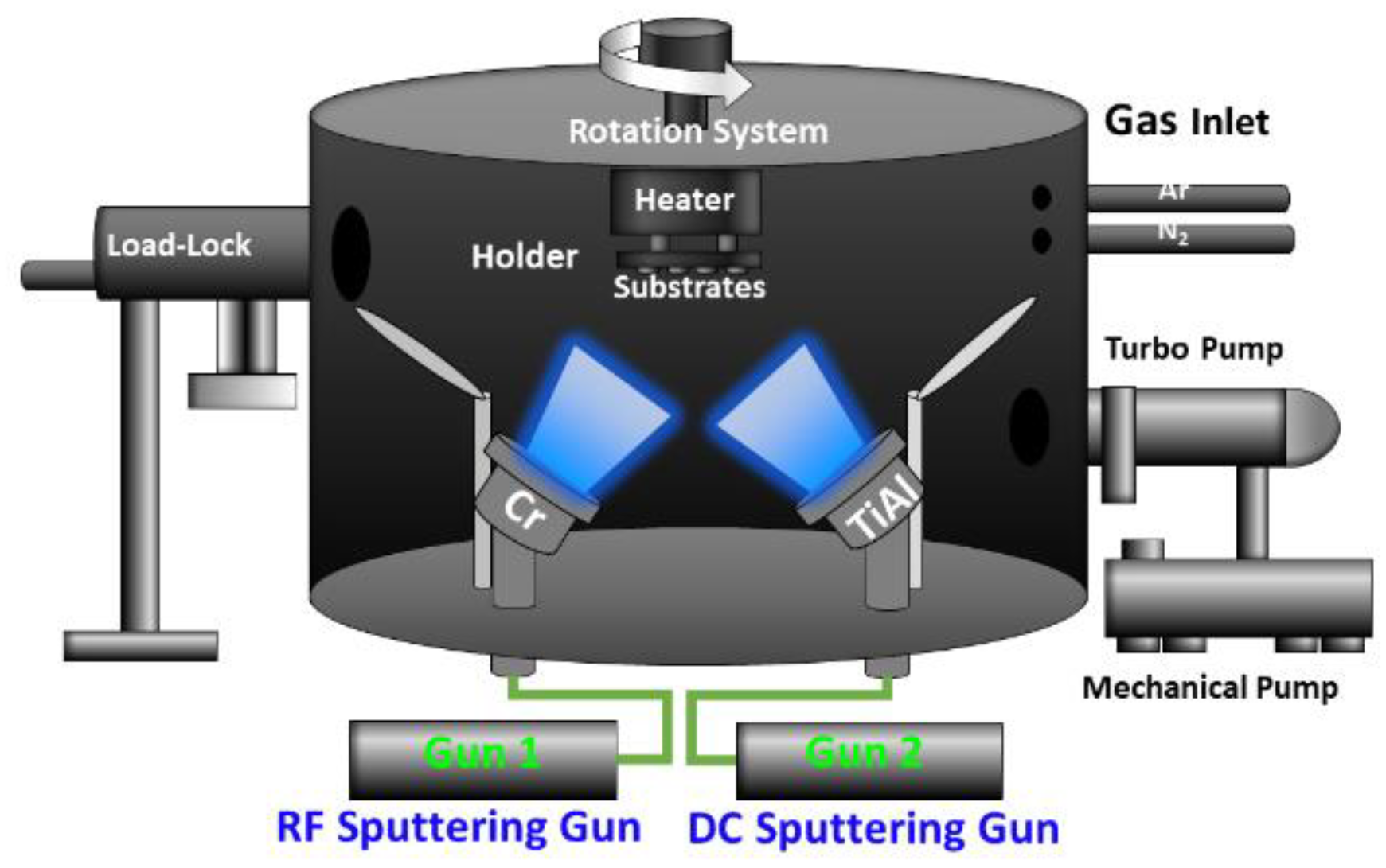
2. Materials and Methods

Reactive co-sputtering equipment was used for the deposition of the TiAlCrN thin films on a glass substrate. The sputtering equipment has two magnetrons located at the bottom of the chamber, geometrically arranged in a confocal configuration (see Figure 1). Each magnetron was tilted 30 degrees off normal and directed to the substrate holder at a diagonal distance of 10 cm. Prior to deposition, the glass substrate was cleaned with two consecutive 15 min ultrasonic baths, first in ethyl acetate and then in isopropanol.
To obtain TiAlCrN coatings with different Cr concentrations, we chose to use two targets, one of Cr and the other of Ti50Al50 (atomic percentage), both with 99.95% purity and 4″ in diameter. The Ti50Al50 target was placed in the magnetron that was connected to the pulsed-DC source (40 kHz), with a constant power of 270 W. The Cr target was placed in the magnetron that was connected to the RF source (13.56 MHz frequency), with different degrees of power: 0 W, 80 W, 110 W, 140 W, and 170 W. Table 1 summarizes the deposition parameters used to fabricate the TiAlCrN coatings.
Thickness is one of the variables that influence the measurement of the electrical and optical properties of the coatings; for this reason, it must be ensured that the comparison is made between coatings with approximately the same thickness. On average, the thin coatings had a thickness of 222 ± 25 nm, and the thick coatings had a thickness of 1040 ± 40 nm, as shown in Figure 2a. The 200 nm thick coatings were used to study the optical properties, and the 1 μm coatings were used to study the electrical properties. As shown in Table 1, an increase in the power to the Cr target caused a decrease in the deposition time, because the increase in power increases the energy of the argon ions impacting the target surface, thus increasing the sputtering rate (see Figure 2b).
The samples were not etched; therefore, small signals from adventitious carbon and oxygen were detected, and the elementary composition of the coatings was analyzed using an Omicron Nano Tech Auger electron spectroscope, measuring in a range between 400 eV and 1400 eV with 1 eV resolution. The results were analyzed using CasaXPS software. The microstructural characterization was performed via XRD (Bragg-Brentano configuration) using a PANalytical X-ray diffractometer model X’Pert PRO, with a Co-Kα source, a potential difference of 40 kV, and a current of 40 mA. The morphology of the films was studied by means of electron microscopy using a FEI QUANTA 200 scanning electron microscope (SEM) at high vacuum pressure and 30 kV voltage. The thickness and roughness were measured using a DEKTAK 150 profilometer, with a resolution of 0.056 μm and a sweep of 2000 μm, for 120 s. The electrical resistivity was measured at room temperature via the four-point probe method (linear configuration) using a Lucas Signatone four-point resistivity tester, and the current range used was between −100 and 100 µA [29]. The values of the voltage and the current were used to calculate the electrical resistance, and the electrical resistivity was determined using the coatings’ geometry. The optical properties of the thin films were determined at room temperature using a high-performance UV-VIS-NIR Cary 5000 spectrophotometer, within a wavelength range of between 250 and 2500 nm with 1 nm intervals. The optical band gap (Egap), absorption coefficient (α), and extinction coefficient (k) were calculated.

3. Results and Discussion

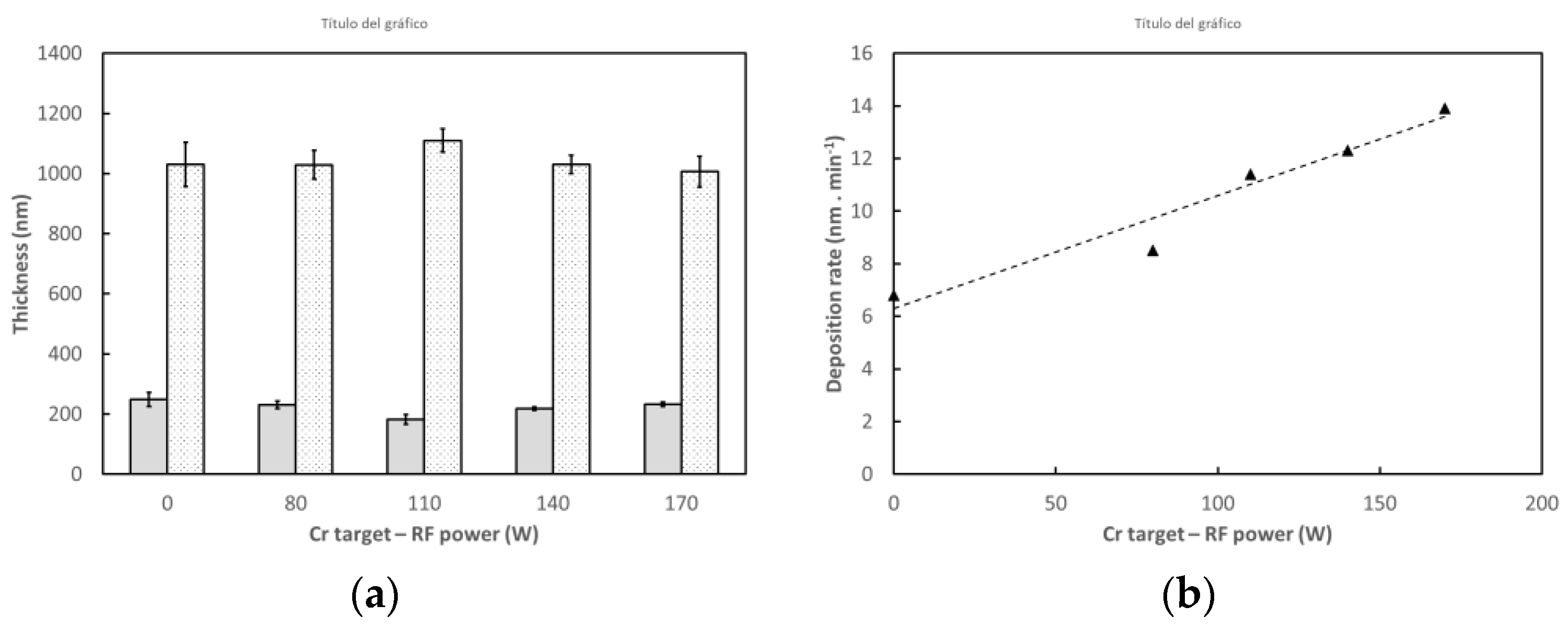
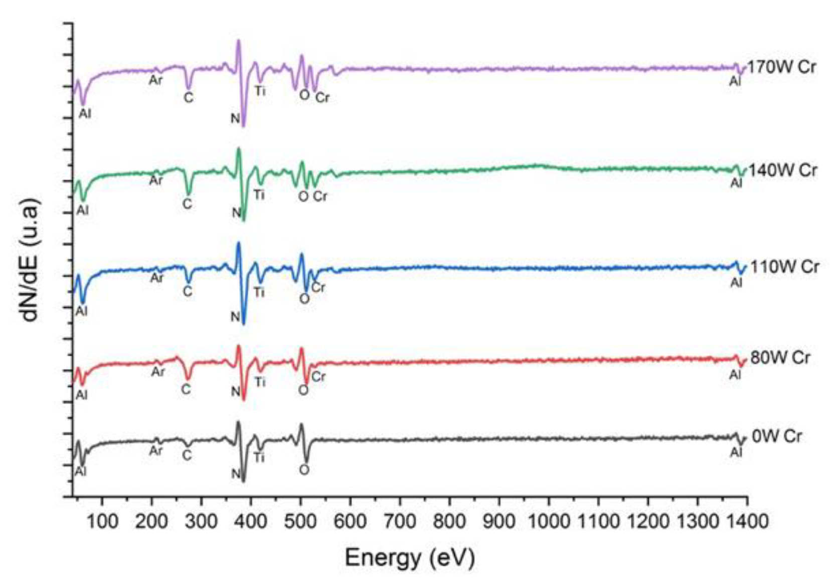
3.1. Elemental Chemical Composition

The AES spectra for the thin (~200 nm) and thick (~1 μm) coatings and the values of the concentrations of each element were practically the same. Therefore, it was considered that the thickness did not affect the chemical composition of the deposited coatings. In the present paper, the analysis of the elemental chemical composition is presented only for the thin (~200 nm) coatings.
Figure 3 shows the resulting AES spectra for the thin TiAlCrN coatings. In the AES spectrum, the presence of coating elements such as aluminum, titanium, chromium, and nitrogen, as well as some impurities such as carbon, oxygen, and argon, can be observed. No argon cleaning was applied at this stage, as it is well known that preferential N sputtering can introduce variations in the surface composition, and therefore small signals from C and O due to surface contamination are observable. However, there might also be an excess of nitrogen on the surface, due to surface contamination or to a nitrogen-terminated surface that influences the Cr content in this paper. Therefore, the Cr amount must be taken as a relative value for comparison between the three different samples. The presence of these impurities in the deposited coatings may be due to surface contamination caused by contact between the surface of the samples and the surroundings or environment, pre-cleaning with argon plasma, or surface passivation and carbon contamination.
Table 2 shows the changes in the relative content of the elements Al, Ti, Cr, and N of the film as a function of the Cr target power. It can be seen that the concentration of nitrogen in the coatings is not affected by the increase in Cr target power, remaining approximately constant (43.6 ± 0.8 at%). The Cr concentration in the coating increases (from 0 at% to 11.6 at%), the Al concentration decreases (from 50.2 at% to 37.5 at%), and the Ti concentration remains approximately constant (7.2 ± 0.2 at%). According to these results, the following nitrides were able to form, considering the formation enthalpies: TiN (−336.6 kJ/mol), AlN (−318 kJ/mol), and CrN (−123.1 kJ/mol) [30,31]. According to the enthalpies of formation, the Ti atoms react more easily with nitrogen, thus rapidly reaching a saturation point at which their concentration remains constant, and the remaining nitrogen reacts with the Al and Cr atoms present in the system.
Similarly, it can be seen that the Al concentration is high compared to that of Ti, although both elements were deposited with the same target and at the same power, a result associated with the high sputtering yield of Al with respect to Ti (1.2 for Al, 0.6 for Ti, and 1.3 for Cr, reference values for ion energies with energy of 600 eV, typical energy of an argon plasma [32]). However, a decrease in aluminum can be seen with increasing power in the Cr target, which could be associated with an atomic substitution of Cr for Al in the material produced.

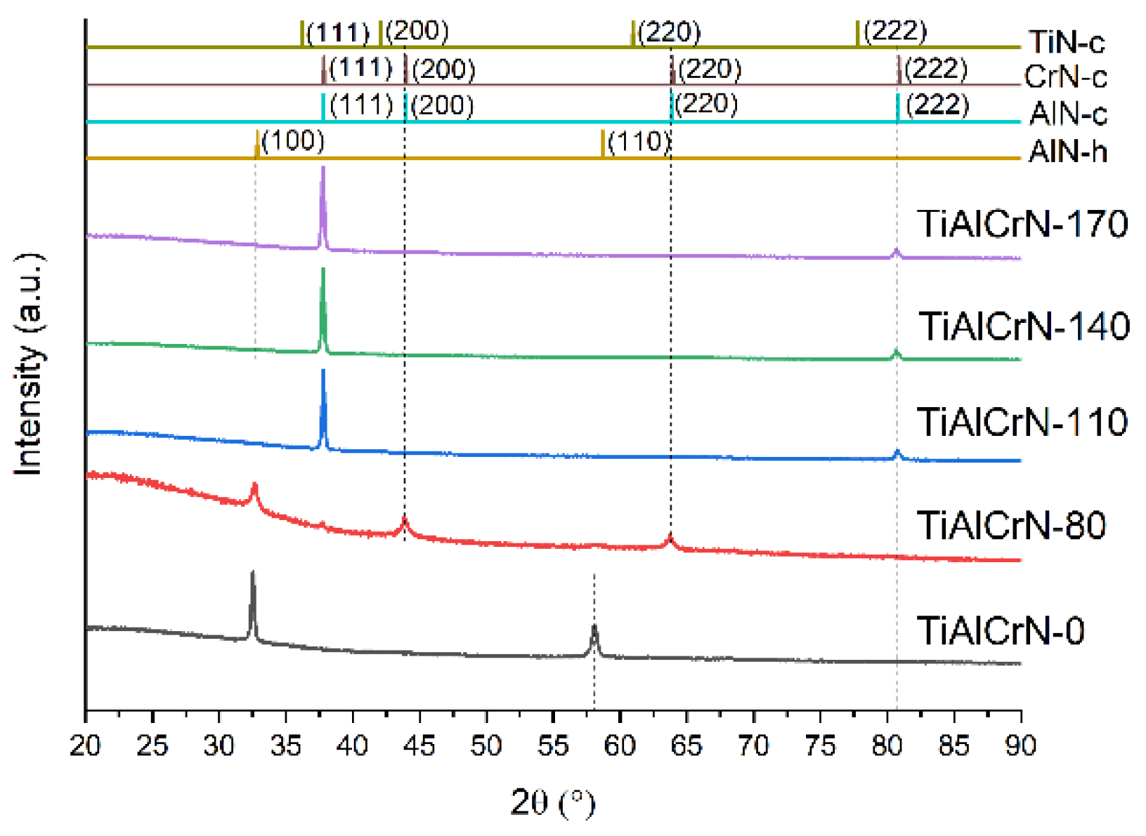
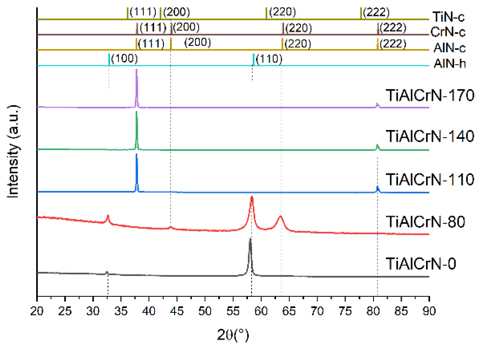
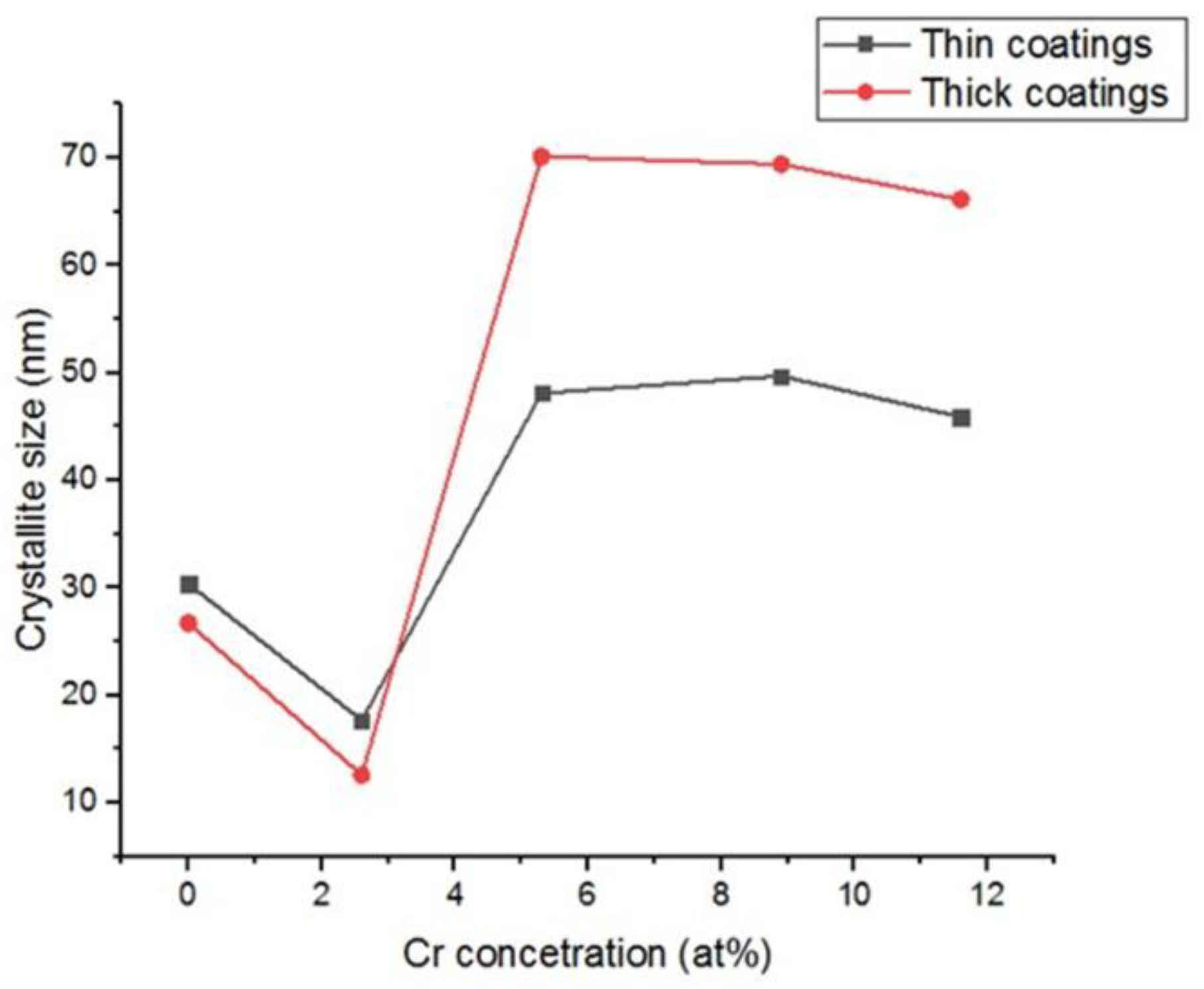
3.2. Crystalline Structure
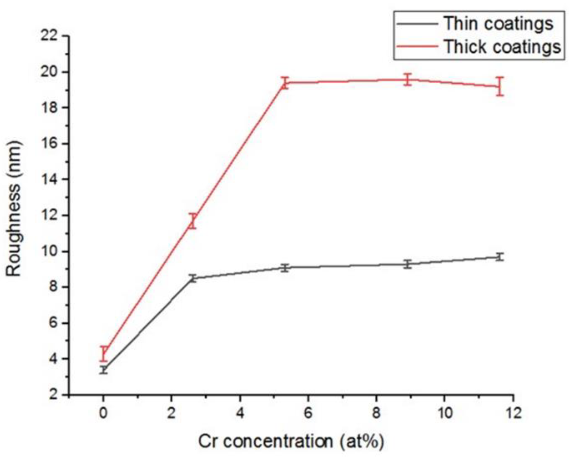
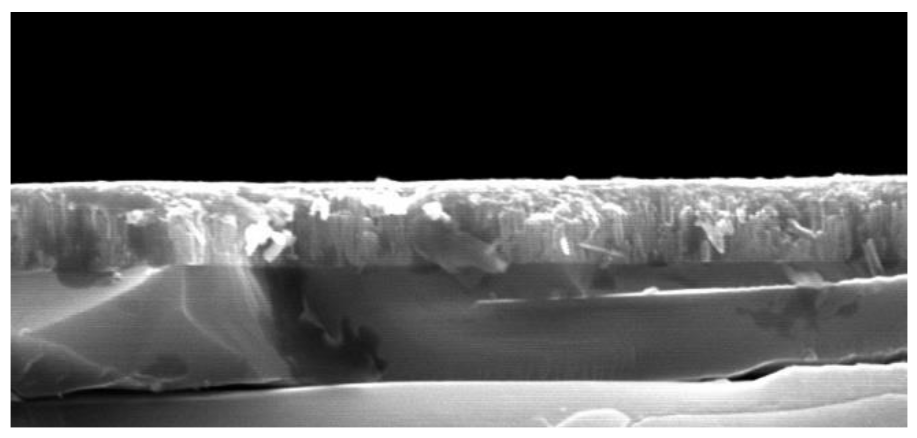
Figure 4 and Figure 5 show the XRD spectra of the thin coatings (thickness 222 ± 25 nm) and thick coatings (thickness 1040 ± 40 nm) as a function of the Cr concentration, with some peaks corresponding to the structures of TiN-c, CrN-c, AlN-c, and AlN-h structures, from crystallographic charts PDF04-017-6803, PDF04-015-0334, PDF00-025-1495, and PDF01-070-2543, respectively. It can be seen in both figures that the increase in Cr concentration has an influence on the crystalline structure of the coating, changing from a hexagonal wurtzite-type structure to a cubic NaCl-type one. Furthermore, the thick coatings (Figure 5) are characterized by exhibiting a greater intensity than the thin coatings (Figure 4), possibly due to a decrease in defects and an increase in grain size with the increasing coating thickness, which is characteristic of films deposited by means of sputtering.
In Figure 4 it can be seen that the coatings with a Cr concentration of 0 at% (TiAlCrN-0) exhibited a single-phase hexagonal wurtzite crystalline structure with preferential orientation along the (100) plane. This hexagonal structure occurs when the Al concentration exceeds the solubility limit of Al in the TiAlN solid solution [33,34]. The representative peaks are located at 2θ angles of 32.5° and 58.1°, which are close to the peaks related to the (100) and (110) planes of the wurtzite hexagonal AlN phase, respectively. These peaks show a slight shift toward smaller 2θ angles, indicating an increase in the lattice parameter, probably caused by the incorporation of large Ti atoms into the AlN structure to form the TiAlN solid solution [35]. In Figure 5, for the same Cr concentration, it can be seen that the same wurtzite phase is detected; however, there is a change of texture: for instance, in the thick film there is a TiAlCrN-0 preferentially oriented along (110), while that of the thin film is preferentially oriented along (100), possibly due to changes in the surface and the strain energy during the film’s growth.
The coatings with a Cr concentration of 2.6 at% (TiAlCrN-80) exhibit a biphasic structure, a wurtzite-type hexagonal phase, and an NaCl-type cubic phase; additionally, the intensity of the peaks is the lowest among the coatings obtained, indicating their low crystallinity. This biphasic structure is related to the transition from the hexagonal wurtzite phase to the cubic NaCl-type phase of the coating, an effect owing to the decrease in the Al concentration to a point that would represent the solubility limit of the Al in the deposited coating; such an effect has been observed in previous studies [18,36]. Its three representative peaks are found at 2θ angles of 32.61°, 43.86°, and 63.69°. The first one is related to the (100) plane of the hexagonal AlN phase, while the second and third are located between the (200) and (220) planes of the cubic CrN, TiN, and AlN phases, indicating a possible formation of a cubic TiAlCrN solid solution.
Coatings with Cr concentrations between 5.3 at% and 11.6 at% (TiAlCrN-110, TiAlCrN-140, and TiAlCrN-170) exhibited a highly in-plane-oriented NaCl-type cubic single-phase crystal structure (111). The presence of this structure is related to an Al concentration below the solubility limit of Al in the coating. The peaks of these coatings are located at 2θ angles of 37.8° and 80.7°, related to the (111) and (222) planes, found displaced at higher angles compared to the TiN reference peaks and at slightly lower angles compared to the CrN and AlN references. This indicates the possible formation of a solid solution of TiN, AlN, and CrN. Similar behavior has been observed in previous studies [32,37]. On the other hand, the coatings with a Cr concentration higher than 9 at% exhibited a high preferential orientation along the (111) plane, which indicates that the increase in the chromium content increases the deformation energy [38].
The crystallite size of the thin films was estimated from the Scherrer formula [39]. Figure 6 shows the crystallite size as a function of the Cr concentration for the thin and thick coatings. The crystallite size for the thin coatings (thickness of 222 ± 25 nm) was in the range of between 17 nm and 45.9 nm, and for the thick coatings (1040 ± 40 nm), it was between 12 nm and 66.1 nm.
The smallest crystallite size was exhibited by the coatings with a Cr concentration of 2.6 at%. (TiAlCrN-80). These coatings were characterized by exhibiting a biphasic structure, a hexagonal wurtzite phase, and a cubic NaCl phase. This behavior could be related to the transition process from the hexagonal wurtzite-type crystalline structure to a cubic NaCl-type one, due to a competitive growth between the two phases that generates grain refinement. This behavior was observed in an investigation by Xu et al. [18], in which TiAlCrN coatings were produced by means of sputtering and a grain refinement was observed in the coatings with a two-phase structure (hexagonal wurtzite-type and cubic NaCl-type) with respect to the single-phase cubic coatings.
The crystallite size increased when the Cr concentration increased to 9 at%. This behavior occurs because there is no longer a competitive growth between two phases, as all the coatings with Cr concentration equal to or higher than 5.3 at% exhibited a highly oriented cubic NaCl-type single-phase structure. Additionally, the increase in crystallite size could be associated with the formation of a TiAlCrN solid solution when added. Thomas et al. [40] fabricated metastable solid solution copper-tungsten films and observed the same behavior: the crystallite size increased with the addition of Cu.

3.3. Roughness

Figure 7 shows the surface roughness of the manufactured coatings as a function of the Cr content. There is a tendency for the roughness to increase with the increasing Cr concentration in the coating. Additionally, it can be seen that a change in the crystallite size causes variations in the average roughness and exhibits the same tendency. This behavior has also been observed in previous studies, in which it was observed that the addition of metallic elements and the discharge power favor the increase in defects and consequently the increase in roughness [41].
According to the deposition parameters, the microstructure of the coatings produced in this investigation corresponds to the T-zone of the J.A. Thornton zone model [42]. This corresponds to a columnar growth, in which there is an increase in residual stresses and roughness with an increase in film thickness.
Another factor influencing surface roughness is surface defects. Figure 8 shows that the Cr-free coatings (TiAlCrN-0) exhibited a surface with fewer defects, characteristic of hard coatings manufactured via PVD deposition techniques such as droplets. The increase in Cr concentration may be generating an increase in these defects through the generation of arcs in the chromium target [43]. Figure 9 show the cross section of the TiAlCrN-110 sample which can be seen as a column grown and with good adherence between the coating and the substrate.

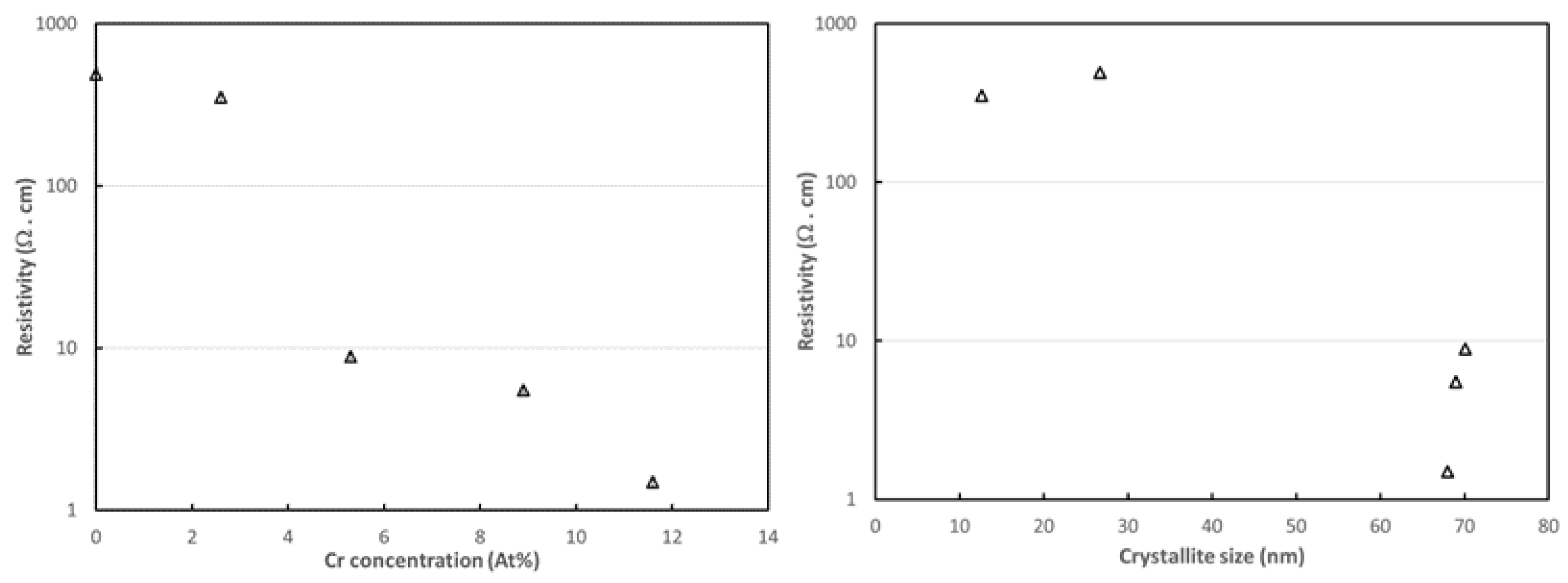
3.4. Electrical Properties

Figure 10 shows the surface electrical resistivity as a function of the Cr concentration. In general, a linear tendency was observed for the voltage and current measured, which corresponds to the ohmic behavior of the coating. The surface electrical resistivity decreases from 490.1 ± 43.4 Ωcm to 1.5 ± 0.1 Ωcm when the Cr concentration increases. These resistivities are within the range of semiconducting materials [44], and their values are within the order of resistivities reported for TiAlN coatings [45].
A decrease in electrical resistivity is seen when the Cr concentration increases. This effect could be due to the transition of a hexagonal wurtzite-type structure to a cubic NaCl-type one, Cr substitution for Al, and the increase in crystallite size. With the decreasing crystallite size, more grains occupy the same volume of material, exhibiting higher zones of boundary grains, which increases the electrical resistivity. In materials with nanometer dimensions, the grain boundaries act as additional scattering centers for the conduction electrons [46].
Additionally, investigations by Zhou et al. [45] and Kassavetis at al. [47] on TiAlN coatings with varying Al contents also recorded a change in the crystal structure from a cubic to a hexagonal structure with increasing aluminum. In those investigations, the hexagonal phase exhibited very high resistivity compared to the cubic phase, as observed in the present investigation. This behavior could be due to the fact that the wurtzite-AlN phase is characterized by the broadest bandgap among semiconductors (6.2 eV at room temperature) [48].

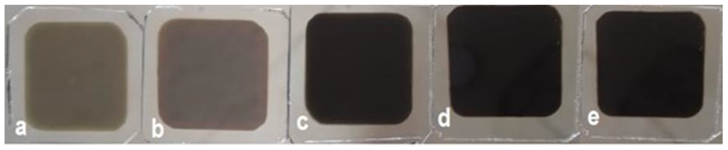
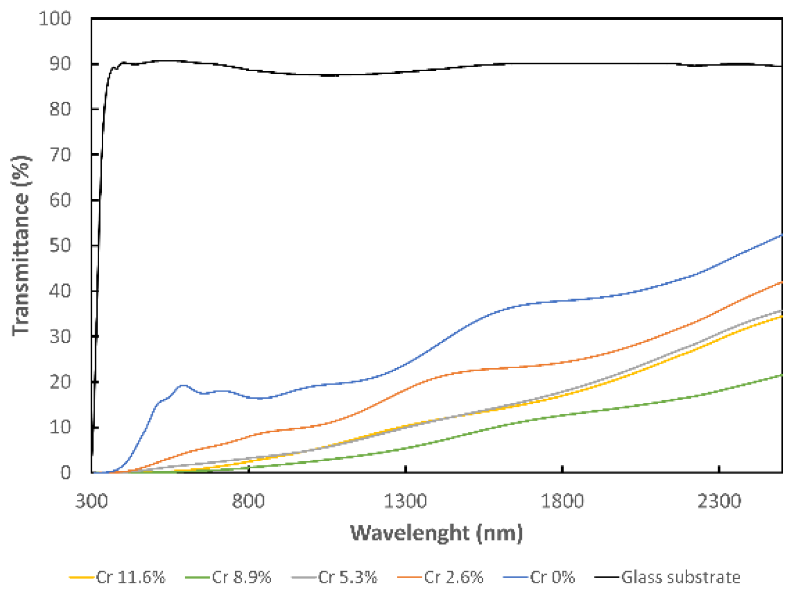
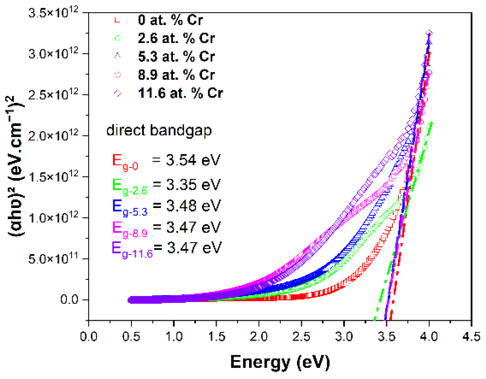
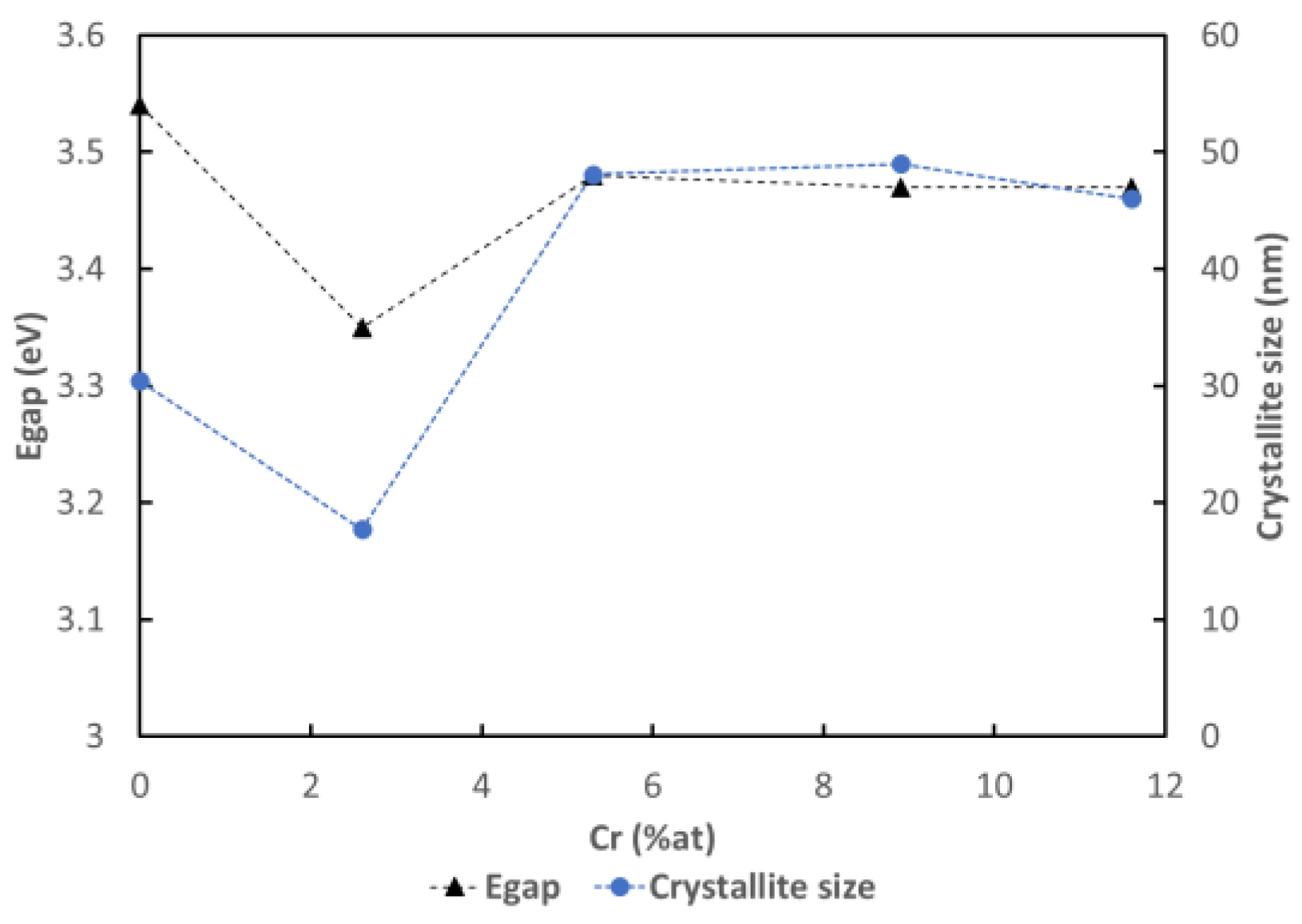
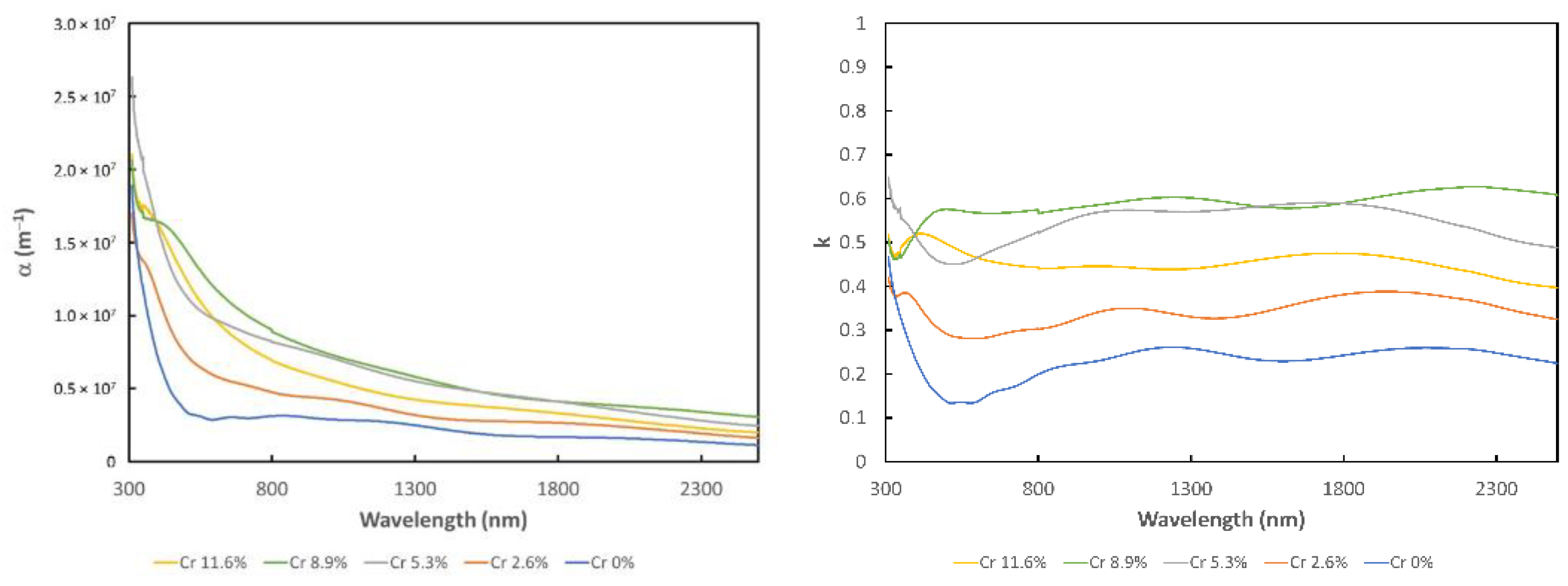
3.5. Optical Properties

Figure 11 shows the appearance of TiAlCrN coatings with thicknesses of 222 ± 25 nm, deposited on glass and as a function of the Cr concentration (to the left lower concentration and to the right higher concentration). The coatings increase their opacity as the Cr concentration increases, transforming from a semi-translucent brown/yellow when the Cr concentration is zero (Figure 11a) to an opaque brown when the chromium reaches a concentration of 11.6 at% (Figure 11e).
Figure 12 shows the optical transmittance spectra of the TiAlCrN coatings. It can be seen that the transmittance decreases when the Cr concentration increases. The transmittance spectra show a tendency to decrease in magnitude over the entire spectrum, evaluated as the Cr concentration increases and the Al concentration decreases. This behavior is similar to those observed in previous studies for TiAlN coatings [49,50], where the decrease in Al concentration led to a decrease in transmittance because of the increase in the crystallite size. The decrease in transmittance with the increasing Cr concentration may be related to the increase in the crystallite size and the increase in the roughness of the coatings’ surface, because grain boundaries and surface roughness are the main light scattering mechanisms [51].
TiAlCrN-0 coatings (CR concentration 0 at%) exhibited the highest transmittance and some interference fringes in the visible region. These fringes result from the constructive and destructive interference of reflected beams at the air/TiAlCrN and TiAlCrN/glass interfaces, peaking in the yellow-orange region (590 nm). These fringes were also observed for the TiAlN coatings with a high Al concentration, which disappear with the decreasing Al concentration [50].
The optical band gap energy (Egap) of the TiAlCrN coatings was determined from the Tauc equation [52] (Equation (1)) for the direct band gap
(α.hν)2 = A(hν − Egap)
where α is the absorption coefficient, hν is the incident photon energy, and A is a constant.
The optical band gap was then estimated using Tauc plots ((αhν)2 vs. (hν)) and extrapolating the linear portion of the curve to the photon energy axis, as shown in Figure 13. It can be seen that the Cr concentration tends to be constant at the optical Egap, approximately 3.5 eV. The obtained optical Egap values are in agreement with those reported for TiAlN coatings fabricated via sputtering [50], where the direct optical Egap ranged between 3.4 eV and 5.2 eV for films with a thickness of 100 nm. The Egap values are a response to the structure of the material. The synthetized TiAlCrN coating exhibits a hexagonal wurtzite crystal structure, and the high values of the Egap obtained could be due to the fact that the wurtzite-AlN phase is characterized by the broadest bandgap among semiconductors (6.2 eV at room temperature) [48].
Figure 14 shows the calculated optical Egap and the crystallite size as a function of the Cr concentration. It can be seen that the Egap tends to be constant in the thin samples; despite this, a slight correlation can be observed between the behavior of the Egap and the crystallite size. In Figure 14, it can be seen that the addition of a low percentage of chromium (2.6%) decreased the value of the crystallite size and the Egap of the samples. From this value, it can be deduced that an increase in the percentage of chromium involves the substitution of aluminum in the coating. This behavior could be because the Cr acts as a dopant impurity, which gives rise to a band of states or impurities within the gap, and the wavefunctions of the electrons bound to the impurity atoms start to overlap as the density of the impurities increases [53]. Furthermore, this has been observed in previous investigations of TiAlN coatings [25,50], in which a decrease in aluminum concentration led to an increase in the crystallite size and, with this, a decrease in the optical Egap [54,55].
The absorption coefficient was calculated using the Lambert-Beer-Bouguer law α = ln (1/T)/d [56,57] and the extinction coefficient (k). Figure 15 shows the absorption coefficient (α), refractive index (n), and extinction coefficient (k) of the TiAlCrN coatings as a function of the Cr concentration.
The absorption coefficient (α) and the extinction coefficient (k) are within the range of values obtained in previous investigations by Schüler et al. [58] and Barshilia et al. [59]. In these papers, TiAlN coatings were deposited by means of sputtering, and they observed that the coatings with the highest Al content exhibited the lowest absorption coefficient (α) and extinction coefficient (k) [58], the same behavior as is observed in the present investigation.

4. Conclusions

TiAlCrN coatings were synthetized using a reactive co-sputtering process. The Cr concentrations were controlled by modifying the power to the Cr target.
Regarding the effects of the variation in Cr concentration, between 0 at% and 11.6 at% on the microstructure and the electrical and optical properties of Ti-Al-Cr-N thin films prepared via reactive co-sputtering, the following conclusions can be stated:
The Ti concentrations remained constant, and the Al concentrations decreased as the Cr concentration in the deposited coatings increased.
The microstructure of the coatings showed a transition from a hexagonal wurtzite structure to a cubic NaCl-type phase as the Cr concentration increased. This transition is related to the decrease in the Al concentration and its solubility limit in the coating.
The crystallite size and the roughness of the deposited coatings exhibited an increasing trend with the increasing Cr concentration.
The increase in the concentration of chromium decreased the values of the surface electrical resistivity of the produced coatings, going from a resistivity of 490.1 ± 43.4 Ωcm to 1.5 ± 0.1 Ωcm for Cr atomic concentrations from 0% to 21%, respectively. All of the fabricated coatings exhibited ohmic behavior at room temperature and within the experimentally evaluated current range (−100 uA, 100 uA).
Increasing the Cr concentration in the TiAlCrN coatings decreased the optical transmittance, and the optical band gap energy (Egap) was approximately 3.5 eV.

Author Contributions

Conceptualization, J.O. and O.P.; methodology, J.O., O.P. and G.P.-N.; validation, G.P.-N., O.P. and J.O.; data curation, formal analysis, software, writing—original draft preparation, G.P.-N.; investigation, G.P.-N. and F.V.; resources, Y.P.; writing—review and editing, G.P.-N., O.P. and J.O.; visualization, G.P.-N.; supervision, O.P., J.O. and Y.P. All authors have read and agreed to the published version of the manuscript.

Funding

This research was funded by MINCIENCIAS, the project “Fabricación y reutilización de herramientas de metal duro a través de decapado y depósito de recubrimientos nanoestructurados obtenidos mediante cosputtering” is identified by the Code 1109-808-63425, Contract: 202-2019.

Acknowledgments

To the “Grupo de investigación en Corrosión, Tribología y Energía” of the Universidad Nacional de Colombia.

Conflicts of Interest

The authors declare no conflict of interest.

References

  1. Beck, U.; Reiners, G.; Kopacz, U.; Jehn, H.A. Decorative hard coatings: Interdependence of optical, stoichiometric and structural properties. Surf. Coat. Technol. 1993, 60, 389–395. [Google Scholar] [CrossRef]
  2. Bouzakis, K.D.; Michailidis, N.; Skordaris, G.; Bouzakis, E.; Biermann, D.; M’Saoubi, R. Cutting with coated tools: Coating technologies, characterization methods and performance optimization. CIRP Ann. 2012, 61, 703–723. [Google Scholar] [CrossRef]
  3. Manaud, J.P.; Poulon, A.; Gomez, S.; Le Petitcorps, Y. A comparative study of CrN, ZrN, NbN and TaN layers as cobalt diffusion barriers for CVD diamond deposition on WC–Co tools. Surf. Coat. Technol. 2007, 202, 222–231. [Google Scholar] [CrossRef]
  4. Dimitriadis, C.A. Characteristics of TiNx/n-Si Schottky diodes deposited by reactive magnetron sputtering. J. Appl. Phys. 1999, 85, 4238–4242. [Google Scholar] [CrossRef]
  5. Cimalla, V.; Pezoldt, J.; Ambacher, O. Group III nitride and SiC based MEMS and NEMS: Materials properties, technology and applications. J. Phys. D Appl. Phys. 2007, 40, 6386–6434. [Google Scholar] [CrossRef]
  6. Matenoglou, G.M.; Koutsokeras, L.E.; Patsalas, P. Plasma energy and work function of conducting transition metal nitrides for electronic applications. Appl. Phys. Lett. 2009, 94, 152108. [Google Scholar] [CrossRef]
  7. Koutsokeras, L. Growth, Structure and Electronic Properties of Ternary Transition Metal Nitrides Thin Films. Ph.D. Thesis, University of Ioannina, Corfu, Greece, 2010. [Google Scholar]
  8. Patsalas, P.; Kalfagiannis, N.; Kassavetis, S.; Abadias, G.; Bellas, D.V.; Lekka, C.; Lidorikis, E. Conductive nitrides: Growth principles, optical and electronic properties, and their perspectives in photonics and plasmonics. Mater. Sci. Eng. R Rep. 2018, 123, 1–55. [Google Scholar] [CrossRef]
  9. Hofmann, S. Formation and diffusion properties of oxide films on metals and on nitride coatings studied with Auger electron spectroscopy and X-ray photoelectron spectroscopy. Thin Solid Film. 1990, 193–194, 648–664. [Google Scholar] [CrossRef]
  10. Hauert, R.; Patscheider, J. From Alloying to Nanocomposites—Improved Performance of Hard Coatings. Adv. Eng. Mater. 2000, 2, 247–259. [Google Scholar] [CrossRef]
  11. Fox-Rabinovich, G.S.; Kovalev, A.I.; Aguirre, M.H.; Beake, B.D.; Yamamoto, K.; Veldhuis, S.C.; Endrino, J.L.; Wainstein, D.L.; Rashkovskiy, A.Y. Design and performance of AlTiN and TiAlCrN PVD coatings for machining of hard to cut materials. Surf. Coat. Technol. 2009, 204, 489–496. [Google Scholar] [CrossRef]
  12. Yamamoto, K.; Sato, T.; Takahara, K.; Hanaguri, K. Properties of (Ti,Cr,Al)N coatings with high Al content deposited by new plasma enhanced arc-cathode. Surf. Coat. Technol. 2003, 174–175, 620–626. [Google Scholar] [CrossRef]
  13. Harris, S.G.; Doyle, E.D.; Vlasveld, A.C.; Audy, J.; Quick, D. A study of the wear mechanisms of Ti1-xAlxN and Ti1-x-yAlxCryN coated high-speed steel twist drills under dry machining conditions. Wear 2003, 254, 723–734. [Google Scholar] [CrossRef]
  14. Fox-Rabinovich, G.S.; Yamomoto, K.; Veldhuis, S.C.; Kovalev, A.I.; Dosbaeva, G.K. Tribological adaptability of TiAlCrN PVD coatings under high performance dry machining conditions. Surf. Coat. Technol. 2005, 200, 1804–1813. [Google Scholar] [CrossRef]
  15. Musil, J. Hard and superhard nanocomposite coatings. Surf. Coat. Technol. 2000, 125, 322–330. [Google Scholar] [CrossRef]
  16. Musil, J.; Vlčekb, J. Magnetron sputtering of films with controlled texture and grain size. Mater. Chem. Phys. 1998, 54, 116–122. [Google Scholar] [CrossRef]
  17. Sigmund, P. Recollections of fifty years with sputtering. Thin Solid Film. 2012, 520, 6031–6049. [Google Scholar] [CrossRef]
  18. Xu, Y.X.; Riedl, H.; Holec, D.; Chen, L.; Du, Y.; Mayrhofer, P.H. Thermal stability and oxidation resistance of sputtered Ti-Al-Cr-N hard coatings. Surf. Coat. Technol. 2017, 324, 48–56. [Google Scholar] [CrossRef]
  19. Tam, P.L.; Zhou, Z.F.; Shum, P.W.; Li, K.Y. Structural, mechanical, and tribological studies of Cr-Ti-Al-N coating with different chemical compositions. Thin Solid Film. 2008, 516, 5725–5731. [Google Scholar] [CrossRef]
  20. Yang, S.; Teer, D.G. Properties and Performance Crtialn of Multilayer Hard Coatings Deposited Using Magnetron Sputter Ion Plating. Surf. Eng. 2002, 18, 391–396. [Google Scholar] [CrossRef]
  21. Fernandes, F.; Danek, M.; Polcar, T.; Cavaleiro, A. Tribological and cutting performance of TiAlCrN films with different Cr contents deposited with multilayered structure. Tribol. Int. 2018, 119, 345–353. [Google Scholar] [CrossRef]
  22. Witit-anun, N.; Buranawong, A.; Chaikhun, S. Effect of nitrogen flow rate on structure of TiCrN thin films prepared from mosaic target by rective dc unbalanced magnetron sputtering. Phranakhon Rajabhat Res. J. Sci. Technol. 2018, 13, 38–49. [Google Scholar]
  23. Valleti, K.; Murali Krishna, D.; Joshi, S.V. Functional multi-layer nitride coatings for high temperature solar selective applications. Sol. Energy Mater. Sol. Cells 2014, 121, 14–21. [Google Scholar] [CrossRef]
  24. Valleti, K.; Krishna, D.M.; Reddy, P.M.; Joshi, S.V. Solar Energy Materials & Solar Cells High temperature stable solar selective coatings by cathodic arc PVD for heat collecting elements. Sol. Energy Mater. Sol. Cells 2016, 145, 447–453. [Google Scholar] [CrossRef]
  25. Pliatsikas, N.; Siozios, A.; Kassavetis, S.; Vourlias, G.; Patsalas, P. Optical properties of nanostructured Al-rich Al1-xTixN films. Surf. Coat. Technol. 2014, 257, 63–69. [Google Scholar] [CrossRef]
  26. Prieto-Novoa, G.M.; Borja-Goyeneche, E.N.; Olaya-Florez, J.J. Efecto del contenido de Ni en las propiedades ópticas y eléctricas de recubrimientos ZrTiSiNiN depositados por co-sputtering. Rev. Acad. Colomb. Ci. Exact. 2019, 43, 366–374. [Google Scholar] [CrossRef]
  27. Guzman Palacios, A.M.; Olaya, J.J.; Alfonso, J.E. Influence of Si on the Structural, Electrical, and Optical Properties of (Al, Ti, Si)N Films Deposited Via Reactive DC Sputtering. Mater. Res. 2020, 23, e20190687. [Google Scholar] [CrossRef]
  28. Vanegas, H.S.; Calderon, P.S.; Alfonso, J.E.; Olaya, J.J.; Ferreira, P.J.; Carvalho, S. Influence of silicon on the microstructure and the chemical properties of nanostructured ZrN-Si coatings deposited by means of pulsed-DC reactive magnetron sputtering. Appl. Surf. Sci. 2019, 481, 1249–1259. [Google Scholar] [CrossRef]
  29. Girotto, E.M.; Santos, I.A. DC electrical resistivity measurements in solids: How to proceed correctly. Quim. Nova 2002, 25, 639–647. [Google Scholar] [CrossRef]
  30. Brandes, E.A.; Brook, G.B. Smithells Metals Reference Book, 7th ed.; Butterworth-Heinemann: Woburn, MA, USA; Elsevier: Amsterdam, The Netherlands, 2013; pp. 8.8–8.16. [Google Scholar]
  31. Danek, M.; Fernandes, F.; Cavaleiro, A.; Polcar, T. Influence of Cr additions on the structure and oxidation resistance of multilayered TiAlCrN films. Surf. Coat. Technol. 2017, 313, 158–167. [Google Scholar] [CrossRef] [Green Version]
  32. Eckstein, W. Sputtering Yields. In Sputtering by Particle Bombardment; Springer: Berlin/Heidelberg, Germany, 2007; pp. 33–187. [Google Scholar] [CrossRef]
  33. Rauch, J.Y.; Rousselot, C.; Martin, N. Structure and composition of TixAl1−xN thin films sputter deposited using a composite metallic target. Surf. Coat. Technol. 2002, 157, 138–143. [Google Scholar] [CrossRef]
  34. Kutschej, K.; Mayrhofer, P.H.; Kathrein, M.; Polcik, P.; Tessadri, R.; Mitterer, C. Structure, mechanical and tribological properties of sputtered Ti1–xAlxN coatings with 0.5 ≤ x ≤ 0.75. Surf. Coat. Technol. 2005, 200, 2358–2365. [Google Scholar] [CrossRef]
  35. Kimura, A.; Hasegawa, H.; Yamada, K.; Suzuki, T. Effects of Al content on hardness, lattice parameter and microstructure of Ti1−xAlxN films. Surf. Coat. Technol. 1999, 120–121, 438–441. [Google Scholar] [CrossRef]
  36. Forsén, R.; Johansson, M.; Odén, M.; Ghafoor, N. Decomposition and phase transformation in TiCrAlN thin coatings. J. Vac. Sci. Technol. A Vac. Surf. Film. 2012, 30, 61506. [Google Scholar] [CrossRef]
  37. Li, T.; Xiong, J.; Guo, Z.; Yang, T.; Yang, M.; Du, H. Structures and properties of TiAlCrN coatings deposited on Ti(C,N)-based cermets with various WC contents. Int. J. Refract. Met. Hard Mater. 2017, 69, 247–253. [Google Scholar] [CrossRef]
  38. Olaya, J.J.; Marulanda, D.M.; Rodil, S. Preferential orientation in metal nitride deposited by the UBM system. Ing. E Investig. 2010, 30, 125–129. [Google Scholar] [CrossRef]
  39. Uvarov, V.; Popov, I. Metrological characterization of X-ray diffraction methods for determination of crystallite size in nano-scale materials. Mater. Charact. 2007, 58, 883–891. [Google Scholar] [CrossRef]
  40. Thomas, K.; Taylor, A.A.; Raghavan, R.; Chawla, V.; Spolenak, R.; Michler, J. Microstructure and mechanical properties of metastable solid solution copper tungsten films. Thin Solid Film. 2017, 642, 82–89. [Google Scholar] [CrossRef]
  41. Ospina, R.; Escobar, D.; Quintero, J.H.; Olaya, J.J.; Mello, A.; Restrepo-Parra, E. Influence of deposition temperature on WTiN coatings tribological performance. Appl. Surf. Sci. 2018, 427, 1096–1104. [Google Scholar] [CrossRef]
  42. Musil, J. Hard nanocomposite coatings: Thermal stability, oxidation resistance and toughness. Surf. Coat. Technol. 2012, 207, 50–65. [Google Scholar] [CrossRef]
  43. Anders, A. Physics of arcing, and implications to sputter deposition. Thin Solid Film. 2006, 502, 22–28. [Google Scholar] [CrossRef]
  44. Schumacher, B.; Bach, H.G.; Spitzer, P.; Obrzut, J. Electrical Properties. In Springer Handbook of Materials Measurement Methods; Springer: Berlin/Heidelberg, Germany, 2006; pp. 431–484. [Google Scholar] [CrossRef]
  45. Zhou, M.; Makino, Y.; Nose, M.; Nogi, K. Phase transition and properties of Ti-Al-N thin films prepared by r.f.-plasma assisted magnetron sputtering. Thin Solid Film. 1999, 339, 203–208. [Google Scholar] [CrossRef]
  46. Marom, H.; Ritterband, M.; Eizenberg, M. The contribution of grain boundary scattering versus surface scattering to the resistivity of thin polycrystalline films. Thin Solid Film. 2006, 510, 62–67. [Google Scholar] [CrossRef]
  47. Kassavetis, S.; Abadias, G.; Vourlias, G.; Bantsis, G.; Logothetidis, S.; Patsalas, P. Optical properties of TixAl1–xN thin films in the whole compositional range. Surf. Coat. Technol. 2016, 295, 125–129. [Google Scholar] [CrossRef]
  48. Vurgaftman, I.; Meyer, J.R.; Ram-Mohan, L.R. Band parameters for III–V compound semiconductors and their alloys. J. Appl. Phys. 2001, 89, 5815–5875. [Google Scholar] [CrossRef] [Green Version]
  49. Luo, H.A.; Lin, Y.; Wang, H.; Hwan Lee, J.; Suvorova, N.A.; Mueller, A.H.; Burrell, A.K.; Mark McCleskey, T.; Bauer, E.; Usov, I.O.; et al. A chemical solution approach to epitaxial metal nitride thin films. Adv. Mater. 2009, 21, 193–197. [Google Scholar] [CrossRef]
  50. Jalali, R.; Parhizkar, M.; Bidadi, H.; Naghshara, H.; Hosseini, S.R.; Jafari, M. The effect of Al content, substrate temperature and nitrogen flow rate on optical band gap and optical features of nanostructured TiAlN thin films prepared by reactive magnetron sputtering. Appl. Phys. A Mater. Sci. Process. 2016, 122, 978. [Google Scholar] [CrossRef]
  51. Apetz, R.; Van Bruggen, M.P.B. Transparent alumina: A light-scattering model. J. Am. Ceram. Soc. 2003, 86, 480–486. [Google Scholar] [CrossRef]
  52. Tauc, J.; Grigorovici, R.; Vancu, A.; Tauc, J.; Grigorovici, R.; Vancu, A. Optical Properties and Electronic Structure of Amorphous Germanium. Phys. Stat. Sol. 1966, 15, 627–637. [Google Scholar] [CrossRef]
  53. Norazlina, M.S.; Shanmugan, S.; Mutharasu, D. Structural and Optical Properties of Chromium Doped Aluminum Nitride Thin Films Prepared by Stacking of Cr Layer on AlN Thin Film. Int. J. Eng. Trends Technol. 2014, 9, 667–670. [Google Scholar] [CrossRef]
  54. Singh, M.; Goyal, M.; Devlal, K. Size and shape effects on the band gap of semiconductor compound nanomaterials. J. Taibah Univ. Sci. 2018, 12, 470–475. [Google Scholar] [CrossRef] [Green Version]
  55. Ramalingam, G.; Kathirgamanathan, P.; Ravi, G.; Elangovan, T.; Manivannan, N.; Kasinathan, K. Quantum Confinement Effect of 2D Nanomaterials. In Quantum Dots-Fundamental and Applications; IntechOpen: London, UK, 2020. [Google Scholar] [CrossRef] [Green Version]
  56. Hasani, E.; Raoufi, D. Influence of temperature and pressure on CdTe: Ag thin film. Surf. Eng. 2018, 34, 915–925. [Google Scholar] [CrossRef]
  57. Raoufi, D.; Taherniya, A. The effect of substrate temperature on the microstructural, electrical and optical properties of Sn-doped indium oxide thin films. Eur. Phys. J. Appl. Phys. 2015, 70, 30302. [Google Scholar] [CrossRef]
  58. Schüler, A.; Thommen, V.; Reimann, P.; Oelhafenet, P. Structural and optical properties of titanium aluminum nitride films (Ti1−xAlxN). J. Vac. Sci. Technol. A Vac. Surf. Film. 2001, 19, 922–929. [Google Scholar] [CrossRef]
  59. Barshilia, H.C.; Selvakumar, N.; Rajam, K.S.; Biswas, A. Optical properties and thermal stability of TiAlN/AlON tandem absorber prepared by reactive DC/RF magnetron sputtering. Sol. Energy Mater. Sol. Cells 2008, 92, 1425–1433. [Google Scholar] [CrossRef]
Figure 1. Scheme of sputtering system used to synthetize the TiAlCrN coatings.
Crystals 12 01831 g001
Figure 2. (a) Thickness of thin and thick TiAlCrN coatings as a function of Cr target power, and (b) Deposition rates of TiAlCrN coatings as a function of Cr target power.
Crystals 12 01831 g002
Figure 3. Auger spectra derived for thin (~200 nm) TiAlCrN coatings.
Crystals 12 01831 g003
Figure 4. XRD spectra of thin TiAlCrN coatings as a function of Cr concentrations.
Crystals 12 01831 g004
Figure 5. XRD spectra of thick TiAlCrN coatings as a function of Cr concentrations.
Crystals 12 01831 g005
Figure 6. Crystallite size as a function of Cr concentration of thin (222 ± 25 nm thick) and thick (1040 ± 40 nm thick) TiAlCrN coatings.
Crystals 12 01831 g006
Figure 7. Surface roughness of TiAlCrN coatings as a function of Cr concentration.
Crystals 12 01831 g007
Figure 8. SEM-SE micrographs at 50,000× of the thin films: (a) TiAlCrN-0, (b) TiAlCrN-80, (c) TiAlCrN-110, (d) TiAlCrN-140, and (e) TiAlCrN-170.
Crystals 12 01831 g008
Figure 9. SEM-SE cross section of TiAlCrN-110 thick coating sample.
Crystals 12 01831 g009
Figure 10. Electrical surface resistivity as a function of Cr content for TiAlCrN coatings.
Crystals 12 01831 g010
Figure 11. Photograph of TiAlCrN coatings from lower to higher Cr concentration. (a) 0 at%; (b) 2.6 at%; (c) 5.3 at%; (d) 8.9 at%, and (e) 11.6 at%.
Crystals 12 01831 g011
Figure 12. Transmittance spectra for thin TiAlCrN coatings as a function of Cr concentration.
Crystals 12 01831 g012
Figure 13. Tauc plots for TiAlCrN coatings as a function of Cr concentration.
Crystals 12 01831 g013
Figure 14. Optical band gap (Egap) for TiAlCrN coatings as a function of Cr concentration.
Crystals 12 01831 g014
Figure 15. Absorption coefficient (α) and extinction coefficient (k) of TiAlCrN coatings.
Crystals 12 01831 g015
Table 1. Deposition parameters used to fabricate the TiAlCrN coatings.
ParameterValues
Cr target—RF power (W)080110140170
Ti50Al50 target—Pulsed DC power (W)270
Deposition time for thin coatings (min)4026202015
Deposition time for thick coatings (min)150120909072
Base pressure (Pa)3 × 10⁻⁴–5 × 10⁻⁴
Working pressure (Pa)0.40 ± 0.05
N2 flux (sccm)3.5
Ar flux (sccm)14
Substrate temperature (K)573 ± 5
Substrate holder rotation speed (rpm)10
Table 2. Calculation of atomic concentration of Al, Ti, Cr, and N from the Auger spectra of thin TiAlCrN coatings.
CoatingCr Target Power (W)Al (at%)Ti (at%)Cr (at%)N (at%)
TiAlCrN-0050.27.00.042.8
TiAlCrN-808046.27.72.643.5
TiAlCrN-11011044.47.25.343.1
TiAlCrN-14014039.07.28.944.8
TiAlCrN-17017037.57.011.643.9
Publisher’s Note: MDPI stays neutral with regard to jurisdictional claims in published maps and institutional affiliations.

