
Synthesis, Evolution of Morphology, Transport Properties for Bi2Te3 Nanoplates
Abstract
:1. Introduction
2. Experimental Sections
2.1. Preparation of Bi2Te3 Nanoplates
2.2. Sample Characterization
3. Results and Discussion
3.1. Structure and Morphology of Bi2Te3 Nanoplates
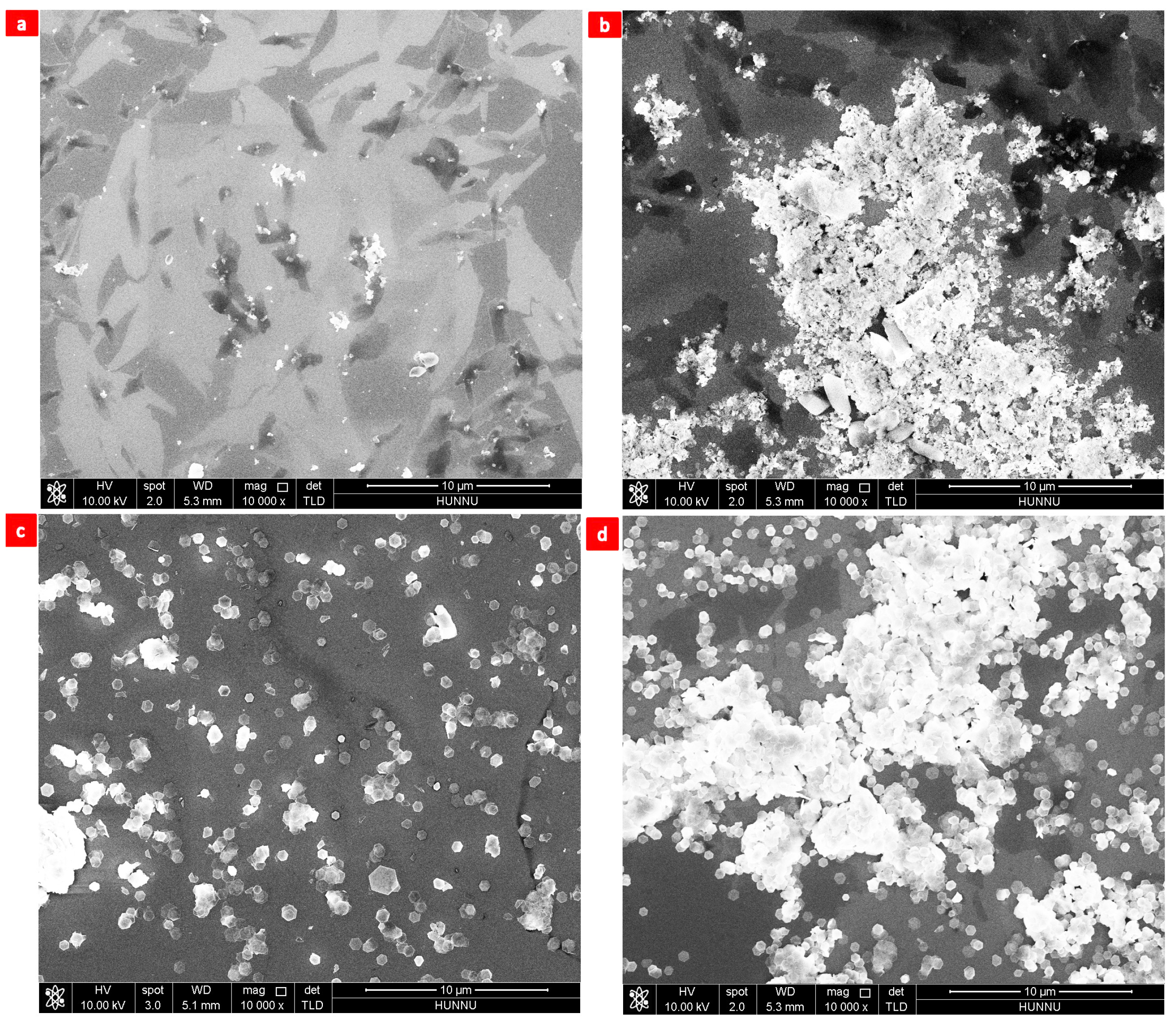
3.2. Influences of the Reaction Temperature
3.3. Influences of the Weight of NaOH
3.4. Influences of the Surfactants
4. Influences of the Reaction Time
5. Transport Properties of Bi2Te3 Solid-State Pellets
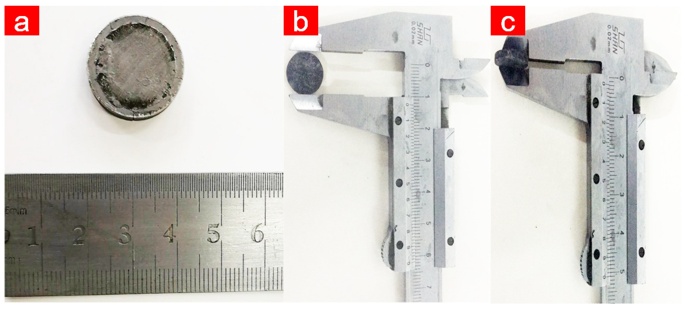
5.1. Density Determination of Solid-State Pellets
5.2. The Electrical Conductivity of Bi2Te3 Solid-State Pellets
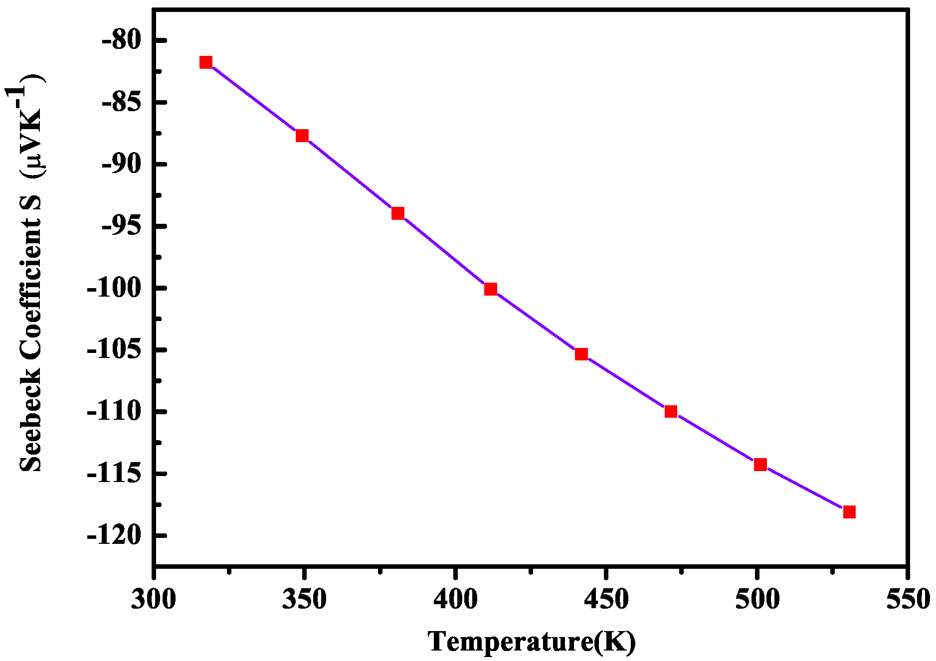
5.3. The Seebeck Coefficient S of Bi2Te3 Solid-State Pellets
6. Conclusions
Author Contributions
Funding
Institutional Review Board Statement
Informed Consent Statement
Data Availability Statement
Conflicts of Interest
References
- Bernevig, B.A.; Hughes, T.L.; Zhang, S.-C. Quantum spin Hall effect and topological phase transition in HgTe quantum wells. Science 2006, 314, 1757–1761. [Google Scholar] [CrossRef] [Green Version]
- Bergerhoff, G.; Hundt, R.; Sievers, R.; Brown, I.D. The inorganic crystal structure data base. J. Chem. Inf. Comput. Sci. 1983, 23, 66–69. [Google Scholar] [CrossRef]
- Allen, F.H.; Shields, G.P. Crystallographic Databases and Knowledge Bases in Materials Design||Graph Set Analysis of Hydrogen Bond Motifs, 1st ed.; Springer: Dordrecht, The Netherlands, 1999; pp. 291–302. [Google Scholar]
- Vergniory, M.G.; Elcoro, L.; Felser, C.; Regnault, N.; Bernevig, B.A.; Wang, Z. A complete catalogue of high-quality topological materials. Nature 2019, 566, 480–485. [Google Scholar] [CrossRef] [PubMed] [Green Version]
- Vergniory, M.G.; Wieder, B.J.; Elcoro, L.; Parkin, S.S.; Felser, C.; Bernevig, B.A.; Regnault, N. All topological bands of all stoichiometric materials. arXiv 2021, arXiv:2105.09954. [Google Scholar] [CrossRef] [PubMed]
- Wieder, B.J.; Bradlyn, B.; Cano, J.; Wang, Z.; Vergniory, M.G.; Elcoro, L.; Soluyanov, A.A.; Felser, C.; Neupert, T.; Regnault, N.; et al. Topological materials discovery from crystal symmetry. Nat. Rev. Mater. 2022, 7, 196–216. [Google Scholar] [CrossRef]
- Wang, J.; Gorini, C.; Richter, K.; Wang, Z.; Ando, Y.; Weiss, D. Two-dimensional-Dirac surface states and bulk gap probed via quantum capacitance in a three-dimensional topological insulator. Nano Lett. 2020, 20, 8493–8499. [Google Scholar] [CrossRef]
- Arimoto, K.; Koretsune, T.; Nomura, K. Quantum anomalous Hall effect in a three-dimensional topological-insulator-thin-film-ferromagnetic-metal heterostructure. Phys. Rev. B 2021, 23, 103. [Google Scholar] [CrossRef]
- Pathak, R.; Dutta, P.; Srivastava, A.; Rawat, D.; Gopal, R.K.; Singh, A.K.; Soni, A.; Biswas, K. Strong Anharmonicity-Induced Low Thermal Conductivity and High n-type Mobility in the Topological Insulator Bi1.1Sb0.9Te2. Angew. Chem. 2022, 134, e202210783. [Google Scholar] [CrossRef]
- Jung, H.; Cho, K.M.; Kim, K.H.; Yoo, H.W.; Al-Saggaf, A.; Gereige, I.; Jung, H.T. Highly efficient and stable CO2 reduction photocatalyst with a hierarchical structure of mesoporous TiO2 on 3D graphene with few-layered MoS2. ACS Sustain. Chem. Eng. 2018, 6, 5718–5724. [Google Scholar] [CrossRef]
- Kuang, P.; Sayed, M.; Fan, J.; Cheng, B.; Yu, J. 3D graphene-based H2-production photocatalyst and electrocatalyst. Adv. Energy Mater. 2020, 10, 1903802. [Google Scholar] [CrossRef]
- Pereira, V.M.; Wu, C.N.; Höfer, K.; Choa, A.; Knight, C.A.; Swanson, J.; Becker, C.; Komarek, A.C.; Rata, A.D.; Rößler, S.; et al. Challenges of topological insulator research: Bi2Te3 thin films and magnetic heterostructures. Phys. Status Solidi 2021, 258, 2000346. [Google Scholar] [CrossRef]
- Balin, K.; Rapacz, R.; Weis, M.; Szade, J. Physicochemical analysis of Bi2Te3–(Fe, Eu)–Bi2Te3 junctions grown by molecular beam epitaxy method. AIP Adv. 2017, 7, 056323. [Google Scholar] [CrossRef] [Green Version]
- Isaeva, A.; Ruck, M. Crystal chemistry and bonding patterns of bismuth-based topological insulators. Inorg. Chem. 2020, 597, 3437–3451. [Google Scholar] [CrossRef]
- Salvato, M.; Crescenzi, M.D.; Scagliotti, M.; Castrucci, P.; Boninelli, S.; Caruso, G.M.; Liu, Y.; Mikkelsen, A.; Timm, R.; Nahas, S.; et al. Nanometric Moiré Stripes on the Surface of Bi2Se3 Topological Insulator. ACS Nano 2022, 16, 13860–13868. [Google Scholar] [CrossRef] [PubMed]
- Kunakova, G.; Kauranens, E.; Niherysh, K.; Bechelany, M.; Smits, K.; Mozolevskis, G.; Bauch, T.; Lombardi, F.; Erts, D. Magnetotransport Studies of Encapsulated Topological Insulator Bi2Se3 Nanoribbons. Nanomaterials 2022, 12, 768. [Google Scholar] [CrossRef] [PubMed]
- Mussler, G. Molecular-Beam Epitaxy of 3D Topological Insulator Thin Films and pelletss on Si Substrates. Phys. Status Solidi 2021, 258, 2000007. [Google Scholar] [CrossRef]
- Thongkham, W.; Lertsatitthanakorn, C.; Jiramitmongkon, K.; Tantisantisom, K.; Boonkoom, T.; Jitpukdee, M.; Sinthiptharakoon, K.; Klamchuen, A.; Liangruksa, M.; Khanchaitit, P. Self-Assembled Three-Dimensional Bi2Te3 Nanowire–PEDOT: PSS Hybrid Nanofilm Network for Ubiquitous Thermoelectrics. ACS Appl. Mater. Interfaces 2019, 11, 6624–6633. [Google Scholar] [CrossRef]
- Plachinda, P.; Hopkins, M.; Rouvimov, S.; Solanki, R. Topological Insulator Bi2Se3 Films on Silicon Substrates. J. Electron. Mater. 2020, 49, 2191–2196. [Google Scholar] [CrossRef]
- Klimovskikh, I.I.; Otrokov, M.M.; Estyunin, D.; Eremeev, S.V.; Filnov, S.O.; Koroleva, A.; Shevchenko, E.; Voroshnin, V.; Rybkin, A.G.; Rusinov, I.P.; et al. Tunable 3D/2D magnetism in the (MnBi2Te4)(Bi2Te3) m topological insulators family. NPJ Quantum Mater. 2020, 5, 54. [Google Scholar] [CrossRef]
- Otrokov, M.M.; Klimovskikh, I.I.; Bentmann, H.; Estyunin, D.; Zeugner, A.; Aliev, Z.S.; Gaß, S.; Wolter, A.U.B.; Koroleva, A.V.; Shikin, A.M.; et al. Prediction and observation of an antiferromagnetic topological insulator. Nature 2019, 576, 416–422. [Google Scholar] [CrossRef]
- Zhang, R.X.; Wu, F.; Sarma, S.D. Möbius insulator and higher-order topology in MnBi2nTe3n+1. Phys. Rev. Lett. 2020, 124, 136407. [Google Scholar] [CrossRef] [PubMed] [Green Version]
- Estyunin, D.A.; Klimovskikh, I.I.; Shikin, A.M.; Schwier, E.F.; Otrokov, M.M.; Kimura, A.; Kumar, S.; Filnov, S.O.; Aliev, Z.S.; Babanly, M.B.; et al. Signatures of temperature driven antiferromagnetic transition in the electronic structure of topological insulator MnBi2Te4. APL Mater. 2020, 8, 021105. [Google Scholar] [CrossRef] [Green Version]
- Yan, J.-Q.; Zhang, Q.; Heitmann, T.; Huang, Z.; Chen, K.Y.; Cheng, J.G.; Wu, W.; Vaknin, D.; Sales, B.C.; McQueeney, R.J. Crystal growth and magnetic structure of MnBi2Te4. Phys. Rev. Mater. 2019, 3, 064202. [Google Scholar] [CrossRef] [Green Version]
- Aliev, Z.S.; Amiraslanov, I.R.; Nasonova, D.I.; Shevelkov, A.V.; Abdullayev, N.A.; Jahangirli, Z.A.; Orujlu, E.N.; Otrokov, M.M.; Mamedov, N.T.; Babanly, M.B.; et al. Novel ternary layered manganese bismuth tellurides of the MnTe–Bi2Te3 system: Synthesis and crystal structure. J. Alloys Compd. 2019, 789, 443–450. [Google Scholar] [CrossRef]
- Hamawandi, B.; Batili, H.; Paul, M.; Ballikaya, S.; Kilic, N.I.; Szukiewicz, R.; Kuchowicz, M.; Johnsson, M.; Toprak, M.S. Minute-made, high-efficiency nanostructured Bi2Te3 via high-throughput green solution chemical synthesis. Nanomaterials 2021, 11, 2053. [Google Scholar] [CrossRef]
- Irfan, S.; Din, M.A.U.; Manzoor, M.Q.; Chen, D. Effect of Co-Doping on Thermoelectric Properties of n-Type Bi2Te3 Nanostructures Fabricated Using a Low-Temperature Sol-Gel Method. Nanomaterials 2021, 11, 2719. [Google Scholar] [CrossRef]
- Chen, J.; Kim, J.; Poudel, N.; Hou, B.; Shen, L.; Shi, H.; Shi, L.; Cronin, S. Enhanced thermoelectric efficiency in topological insulator Bi2Te3 nanoplates via atomic layer deposition-based surface passivation. Appl. Phys. Lett. 2018, 113, 083904. [Google Scholar] [CrossRef] [Green Version]
- Liu, Y.; Wang, Q.; Pan, J.; Sun, Y.; Zhang, L.; Song, S. Hierarchical Bi2Te3 Nanostrings: Green Synthesis and Their Thermoelectric Properties. Chem. A Eur. J. 2018, 24, 9765–9768. [Google Scholar] [CrossRef]
- Singh, S.; Mun, H.; Lee, S.; Kim, S.W.; Baik, S. Giant Peak Voltage of Thermopower Waves Driven by the Chemical Potential Gradient of Single-Crystalline Bi2Te3. Adv. Mater. 2017, 29, 1701988. [Google Scholar] [CrossRef]
- White, M.A.; Medina-Gonzalez, A.M.; Vela, J. Soft Chemistry, Coloring and Polytypism in Filled Tetrahedral Semiconductors: Toward Enhanced Thermoelectric and Battery Materials. Chem. A Eur. J. 2018, 24, 3650–3658. [Google Scholar] [CrossRef]
- Tan, G.; Zhao, L.D.; Kanatzidis, M.G. Rationally designing high-performance bulk thermoelectric materials. Chem. Rev. 2016, 116, 12123–12149. [Google Scholar] [CrossRef] [PubMed]
- Ortega, S.; Ibáñez, M.; Liu, Y.; Zhang, Y.; Kovalenko, M.V.; Cadavid, D.; Cabot, A. Bottom-up engineering of thermoelectric nanomaterials and pelletss from solution-processed nanoparticle building blocks. Chem. Soc. Rev. 2017, 46, 3510–3528. [Google Scholar] [CrossRef] [PubMed] [Green Version]
- He, J.; Tritt, T.M. Advances in thermoelectric materials research: Looking back and moving forward. Science 2017, 357, eaak9997. [Google Scholar] [CrossRef] [PubMed] [Green Version]
- Samanta, M.; Roychowdhury, S.; Ghatak, J.; Perumal, S.; Biswas, K. Ultrahigh Average Thermoelectric Figure of Merit, Low Lattice Thermal Conductivity and Enhanced Microhardness in Nanostructured (GeTe)x(AgSbSe2)100−x. Chem. A Eur. J. 2017, 23, 7438–7443. [Google Scholar] [CrossRef]
- Pan, Y.; Wang, Q.Z.; Yeats, A.L.; Pillsbury, T.; Flanagan, T.C.; Richardella, A.; Zhang, H.; Awschalom, D.D.; Liu, C.X.; Samarth, N. Helicity dependent photocurrent in electrically gated (Bi1−xSbx)2Te3 thin films. Nat. Commun. 2017, 8, 1037. [Google Scholar] [CrossRef] [PubMed] [Green Version]
- Hasan, M.Z.; Kane, C.L. Colloquium: Topological insulators. Rev. Mod. Phys. 2010, 282, 3045–3068. [Google Scholar] [CrossRef] [Green Version]
- Zhang, H.J.; Liu, C.X.; Qi, X.L.; Dai, X.; Fang, Z.; Zhang, S.C. Topological insulators in Bi2Se3, Bi2Te3 and Sb2Te3 with a single Dirac cone on the surface. Nat. Phys. 2009, 5, 438–442. [Google Scholar] [CrossRef]
- Zhou, F.; Zhao, Y.; Zhou, W.; Tang, D. Temperature-Dependent Raman Scattering of Large Size Hexagonal Bi2Se3 Single-Crystal Nanoplates. Appl. Sci. 2018, 8, 1794. [Google Scholar] [CrossRef] [Green Version]
- Zhou, F.; Zhao, Y.; Zhou, W.; Tang, D. Temperature dependent Raman of BiTe nanotubes. AIP Adv. 2018, 8, 125330. [Google Scholar] [CrossRef] [Green Version]
- Tan, G.; Zhao, L.D.; Shi, F.; Doak, J.W.; Lo, S.H.; Sun, H.; Wolverton, C.; Dravid, V.P.; Uher, C.; Kanatzidis, M.G. High thermoelectric performance of p-type SnTe via a synergistic band engineering and nanostructuring approach. J. Am. Chem. Soc. 2014, 136, 7006–7017. [Google Scholar] [CrossRef]
- Biswas, K.; He, J.Q.; Zhang, Q.C.; Wang, G.Y.; Uher, C.; Dravid, V.P.; Kanatzidis, M.G. Strained endotaxial nanostructures with high thermoelectric figure of merit. Nat. Chem. 2011, 3, 160–166. [Google Scholar] [CrossRef] [PubMed]
- Tan, G.J.; Zheng, Y.; Tang, X.F. High thermoelectric performance of nonequilibrium synthesized CeFe4Sb12 composite with multi-scaled nanostructures. Appl. Phys. Lett. 2013, 103, 183904. [Google Scholar] [CrossRef]
- Zhao, L.D.; Wu, H.J.; Hao, S.Q.; Wu, C.I.; Zhou, X.Y.; Biswas, K.; He, J.Q.; Hogan, T.P.; Uher, C.; Wolverton, C.; et al. All-scale hierarchical thermoelectrics: MgTe in PbTe facilitates valence band convergence and suppresses bipolar thermal transport for high performance. Energy Environ. Sci. 2013, 6, 3346–3355. [Google Scholar] [CrossRef]
- Kim, H.S.; Shin, H.S.; Lee, J.S.; Ahn, C.W.; Song, J.Y.; Doh, Y.J. Quantum electrical transport properties of topological insulator Bi2Te3 nanowires. Curr. Appl. Phys. 2016, 16, 51–56. [Google Scholar] [CrossRef] [Green Version]
- Zhu, H.T.; Luo, J.; Liang, J.K. Synthesis of highly crystalline Bi2Te3 nanotubes and their enhanced thermoelectric properties. J. Mater. Chem. A 2014, 2, 12821–12826. [Google Scholar] [CrossRef]
- Fu, J.; Song, S.; Zhang, X.; Cao, F.; Zhou, L.; Li, X.; Zhang, H. Bi2Te3 nanoplates and nanoflowers: Synthesized by hydrothermal process and their enhanced thermoelectric properties. CrystEngComm 2012, 14, 2159–2165. [Google Scholar] [CrossRef]
- Ponraj, J.S.; Xu, Z.Q.; Dhanabalan, S.C.; Mu, H.; Wang, Y.; Yuan, J.; Li, P.; Thakur, S.; Ashrafi, M.; Mccoubrey, K.; et al. Photonics and optoelectronics of two-dimensional materials beyond graphene. Nanotechnology 2016, 27, 462001. [Google Scholar] [CrossRef]
- Wang, Z.; Zhu, W.; Qiu, Y.; Yi, X.; Bussche, A.; Kane, A.; Gao, H.; Koski, K.; Hurt, R. Biological and environmental interactions of emerging two-dimensional nanomaterials. Chem. Soc. Rev. 2016, 45, 1750–1780. [Google Scholar] [CrossRef] [Green Version]
- Hong, M.; Chen, Z.G.; Yang, L.; Zou, J. Enhancing thermoelectric performance of Bi2Te3-based nanostructures through rational structure design. Nanoscale 2016, 8, 8681–8686. [Google Scholar] [CrossRef]
- Li, C.Y.; Ruoff, A.L.; Spencerm, C.W. Effect of pressure on the energy gap of Bi2Te3. J. Appl. Phys. 1961, 32, 1733–1735. [Google Scholar] [CrossRef]
- Kullmann, W.; Geurts, J.; Richter, W.; Lehner, N.; Steigenberger, U.; Eichhorn, G.; Geick, R. Effect of hydrostatic and uniaxial pressure on structural properties and Raman active lattice vibrations in Bi2Te3. Phys. Status Solidi 1984, 125, 131–138. [Google Scholar] [CrossRef]
- Gong, C.; Li, L.; Li, Z.; Ji, H.; Stern, A.; Xia, Y.; Cao, T.; Bao, W.; Wang, C.; Wang, Y.; et al. Discovery of Intrinsic Ferromagnetism in Two-Dimensional van Der Waals Crystals. Nature 2017, 546, 265–269. [Google Scholar] [CrossRef] [PubMed] [Green Version]
- Yuan, H.; Liu, Z.; Xu, G.; Zhou, B.; Wu, S.; Dumcenco, D.; Yan, K.; Zhang, Y.; Mo, S.K.; Dudin, P.; et al. Evolution of the Valley Position in Bulk Transition-Metal Chalcogenides and Their Monolayer Limit. Nano Lett. 2016, 16, 4738–4745. [Google Scholar] [CrossRef] [PubMed] [Green Version]
- Mehta, R.J.; Zhang, Y.; Karthik, C.; Singh, B.; Siegel, R.W.; Borca-Tasciuc, T.; Ramanath, G. A New Class of Doped Nanobulk High-Figure-of-Merit Thermoelectrics by Scalable Bottom-up Assembly. Nat. Mater. 2012, 11, 233–240. [Google Scholar] [CrossRef] [PubMed]
- Shi, B.; Miao, L.; Wang, Q.; Du, J.; Tang, P.; Liu, J.; Zhao, C.; Wen, S. Broadband ultrafast spatial self-phase modulation for topological insulator Bi2Te3 dispersions. Appl. Phys. Lett. 2015, 107, 15110. [Google Scholar] [CrossRef]
- Wang, Q.; Chen, Y.; Miao, L.; Jiang, G.; Chen, S.; Liu, J.; Fu, X.; Zhao, C.; Zhang, H. Wide spectral and wavelength-tunable dissipative soliton fiber laser with topological insulator nano-sheets self-assembly films sandwiched by PMMA polymer. Opt. Express 2015, 23, 7681–7693. [Google Scholar] [CrossRef] [PubMed]
- Dun, C.; Hewitt, C.A.; Jiang, Q.; Guo, Y.; Xu, J.; Li, Y.; Li, Q.; Wang, H.; Carroll, D.L. Bi2Te3 Plates with Single Nanopore: The Formation of Surface Defects and Self-Repair Growth. Chem. Mater. 2018, 30, 1965–1970. [Google Scholar] [CrossRef]
- Yang, Z.; Wang, W.; Pan, J.; Ye, C. Alternating Current Electroluminescent Devices with Inorganic Phosphors for Deformable Displays. Cell Rep. Phys. Sci. 2020, 1, 100213. [Google Scholar] [CrossRef]
- He, Q.; Worku, M.; Xu, L.; Zhou, C.; Lteif, S.; Schlenoff, J.B.; Ma, B. Surface passivation of perovskite thin films by phosphonium halides for efficient and stable solar cells. J. Mater. Chem. A 2020, 8, 2039–2046. [Google Scholar] [CrossRef]
- He, Q.; Worku, M.; Xu, L.; Zhou, C.; Lin, H.; Robb, A.J.; Hanson, K.; Xin, Y.; Ma, B. Facile Formation of 2D–3D Heterojunctions on Perovskite Thin Film Surfaces for Efficient Solar Cells. ACS Appl. Mater. Interfaces 2020, 12, 1159–1168. [Google Scholar] [CrossRef]
- Chen, J.; Zhou, Y.; Fu, Y.; Pan, J.; Bakr, O.M. Oriented Halide Perovskite Nanostructures and Thin Films for Optoelectronics. Chem. Rev. 2021, 121, 12112–12180. [Google Scholar] [CrossRef] [PubMed]
- Srivastava, P.; Singh, K. Morphological evolution in single-crystalline Bi2Te3 nanoparticles, nanosheets and nanotubes with different synthesis temperatures. Bull. Mater. Sci. 2013, 36, 765–770. [Google Scholar] [CrossRef] [Green Version]
- Wei, H.; Wu, H.; Huang, K.; Ge, B.; Ma, J.; Lang, J.; Zu, D.; Lei, M.; Yao, Y.; Guo, W.; et al. Ultralow-temperature photochemical synthesis of atomically dispersed Pt catalysts for the hydrogen evolution reaction. Chem. Sci. 2019, 10, 2830–2836. [Google Scholar] [CrossRef] [PubMed] [Green Version]
- Menke, E.J.; Brown, M.A.; Li, Q.; Hemminger, J.C.; Penner, R.M. Bismuth telluride (Bi2Te3) nanowires: Synthesis by cyclic electrodeposition/stripping, thinning by electrooxidation, and electrical power generation. Langmuir 2006, 22, 10564–10574. [Google Scholar] [CrossRef] [PubMed]
- Zheng, X.F.; Liu, C.X.; Yan, Y.Y.; Wang, Q. A review of thermoelectrics research—Recent developments and potentials for sustainable and renewable energy applications. Renew. Sustain. Energy Rev. 2014, 32, 486–503. [Google Scholar] [CrossRef]
- Zhang, Y.; Hu, L.P.; Zhu, T.J.; Xie, J.; Zhao, X.B. High yield Bi2Te3 single crystal nanosheets with uniform morphology via a solvothermal synthesis. Cryst. Growth Des. 2013, 13, 645–651. [Google Scholar] [CrossRef]
- Liang, Y.; Wang, W.; Zeng, B.; Zhang, G.; Song, Y.; Zhang, X.; Huang, J.; Li, J.; Li, T. The effect of the Bi source on optical properties of Bi2Te3 nanostructures. Solid State Commun. 2011, 151, 704–707. [Google Scholar] [CrossRef]
- He, H.; Huang, D.; Zhang, X.; Li, G. Characterization of hexagonal Bi2Te3 nanosheets prepared by solvothermal method. Solid State Commun. 2012, 152, 810–815. [Google Scholar] [CrossRef]
- Mamur, H.; Bhuiyan, M.R.A.; Korkmaz, F. A review on bismuth telluride (Bi2Te3) nanostructure for thermoelectric applications. Renew. Sustain. Energy Rev. 2018, 82, 4159–4169. [Google Scholar] [CrossRef]
- Takashiri, M.; Kai, S.; Wada, K.; Takasugi, S.; Tomita, K. Role of stirring assist during solvothermal synthesis for preparing single-crystal bismuth telluride hexagonal nanoplates. Mater. Chem. Phys. 2016, 173, 213–218. [Google Scholar] [CrossRef]
- Chen, S.; Cai, K.; Shen, S. Synthesis via a Microwave-Assisted Wet Chemical Method and Characterization of Bi2Te3 with Various Morphologies. J. Electron. Mater. 2016, 45, 1425–1432. [Google Scholar] [CrossRef]
- Zhang, Y.; Chen, H.; Li, Z.; Huang, T.; Zheng, S. Rational design and controlled synthesis of Te/Bi2Te3 heterostructure nanostring composites. J. Cryst. Growth 2015, 421, 13–18. [Google Scholar] [CrossRef]


| TeO2 | Bi2O3 | NaOH | PVP (K-30) | t (h) | T (°C) | Morphology | |
|---|---|---|---|---|---|---|---|
| (a) | 6 mmol | 2 mmol | 0.8 g | 1 g | 7 h | 140 °C | nanoparticles |
| (b) | 6 mmol | 2 mmol | 0.8 g | 1 g | 7 h | 160 °C | nanoparticles and nanoplates |
| (c) | 6 mmol | 2 mmol | 0.8 g | 1 g | 7 h | 180 °C | nanoplates |
| (d) | 6 mmol | 2 mmol | 0.8 g | 1 g | 7 h | 200 °C | nanoplates and nanoclusters |
| TeO2 | Bi2O3 | PVP (K-30) | T (°C) | t (h) | NaOH | Morphology | |
|---|---|---|---|---|---|---|---|
| (a) | 6 mmol | 4 mmol | 1 g | 180 °C | 7 h | 0 g | nanoparticles and nanowires |
| (b) | 6 mmol | 4 mmol | 1 g | 180 °C | 7 h | 0.2 g | nanoparticles, nanowires and nanoplates |
| (c) | 6 mmol | 4 mmol | 1 g | 180 °C | 7 h | 0.4 g | nanowires and nanoplates |
| (d) | 6 mmol | 4 mmol | 1 g | 180 °C | 7 h | 0.8 g | nanoplates |
| (e) | 6 mmol | 4 mmol | 1 g | 180 °C | 7 h | 1.6 g | nanoparticles and nanoplates |
| (f) | 6 mmol | 4 mmol | 1 g | 180 °C | 7 h | KOH | nanoparticles and nanoplates |
| TeO2 | Bi2O3 | T (°C) | t (h) | NaOH | Surfactants | Morphology | |
|---|---|---|---|---|---|---|---|
| (a) | 6 mmol | 4 mmol | 180 °C | 7 h | 0.8 g | 0 g | nanoplates and nanowires |
| (b) | 6 mmol | 4 mmol | 180 °C | 7 h | 0.8 g | CTAB | nanoplates and nanowires |
| (c) | 6 mmol | 4 mmol | 180 °C | 7 h | 0.8 g | EDTA | nanoplates and nanowires |
| (d) | 6 mmol | 4 mmol | 180 °C | 7 h | 0.8 g | SDBS | nanoparticles, nanoplates and nanowires |
| TeO2 | Bi2O3 | NaOH | PVP (K-30) | T (°C) | t (h) | Morphology | |
|---|---|---|---|---|---|---|---|
| (a) | 6 mmol | 2 mmol | 0.8 g | 1 g | 180 °C | 3 h | nanoparticles |
| (b) | 6 mmol | 2 mmol | 0.8 g | 1 g | 180 °C | 5 h | nanoparticles andnanoplates |
| (c) | 6 mmol | 2 mmol | 0.8 g | 1 g | 180 °C | 7 h | nanoplates |
| (d) | 6 mmol | 2 mmol | 0.8 g | 1 g | 180 °C | 9 h | nanoplates |
| (e) | 6 mmol | 2 mmol | 0.8 g | 1 g | 180 °C | 11 h | nothing |
| Parameters Name | M (g) | D (mm) | H (mm) | V (cm3) | ρ (g/cm3) | Relative Density |
|---|---|---|---|---|---|---|
| Measured value | 1.726 | 12.51 | 1.94 | 0.238334 | 7.241938 | 94.1 % |
Publisher’s Note: MDPI stays neutral with regard to jurisdictional claims in published maps and institutional affiliations. |
© 2022 by the authors. Licensee MDPI, Basel, Switzerland. This article is an open access article distributed under the terms and conditions of the Creative Commons Attribution (CC BY) license (https://creativecommons.org/licenses/by/4.0/).
Share and Cite
Zhao, Y.-J.; Zhou, F. Synthesis, Evolution of Morphology, Transport Properties for Bi2Te3 Nanoplates. Crystals 2022, 12, 1668. https://doi.org/10.3390/cryst12111668
Zhao Y-J, Zhou F. Synthesis, Evolution of Morphology, Transport Properties for Bi2Te3 Nanoplates. Crystals. 2022; 12(11):1668. https://doi.org/10.3390/cryst12111668
Chicago/Turabian StyleZhao, Yu-Jing, and Fang Zhou. 2022. "Synthesis, Evolution of Morphology, Transport Properties for Bi2Te3 Nanoplates" Crystals 12, no. 11: 1668. https://doi.org/10.3390/cryst12111668