Article

Numerical Investigation of Optical and Photoelectric Properties for 850 nm VCSELs with Arbitrary Crystal Orientation

School of Information Science and Engineering, Shandong University, Qingdao 266237, China
*
Authors to whom correspondence should be addressed.
Crystals 2022, 12(10), 1459; https://doi.org/10.3390/cryst12101459
Submission received: 26 September 2022 / Revised: 12 October 2022 / Accepted: 13 October 2022 / Published: 15 October 2022

Abstract

:
High-speed VCSELs are widely used for high-capacity, short-range data communication links. Here, we numerically investigate the optical and electronic properties of a crystal orientation-dependent 1.06% compression InGaAs-AlGaAs laser emitting around 850 nm. The reduction of the density of states is observed in the largest energy range for the quantum well in the (110) orientation compared with the conventional (001) orientation. The calculated transparency carrier density decreases from 2.74 × 1018 cm−3 to 1.88 × 1018 cm−3 with the gain coefficient rising from 4969.4 cm−1 to 5427.2 cm−1 in (110) orientation. The 3 dB bandwidth of 31.25 GHz is realized in the (110) orientation, which can support 60 Gbps (NRZ) applications.

1. Introduction

Vertical cavity surface-emitting lasers (VCSELs) are the dominant optical sources for multimode fiber (MMF)-based optical links in data centers, optical storage, short-distance optical communication links, and high-performance computers (HPCs) due to the advantages of low cost, good beam quality, and high modulation speeds at low currents [1,2,3]. With the network traffic exponentially increasing year by year, high-speed and energy-efficient 850 nm VCSELs are required to meet the higher transmission data rates. Initially, conventional 850 nm VCSELs employed unstrained GaAs QWs with AlGaAs as the barrier. The highest data rate of 30 Gbps at 25 °C was reported for a 6µm oxide aperture diameter with GaAs QWs in 2008 [4]. Compared with the conventional unstrained GaAs/AlGaAs quantum wells, InGaAs/AlGaAs strained QWs provide a higher differential gain and lower transparency carrier threshold, which are adopted for modern high-speed VCSELs emitting near 850 nm [5]. According to recent research, a well-designed VCSEL was able to attain a 3 dB modulation bandwidth of 30 GHz at RT and operated at 40–57 Gbps [6,7,8]. However, it is hard to increase the modulation bandwidth further due to the limitation of the resonant frequency, which is primarily determined by the differential gain. A higher differential gain leads to a larger resonance frequency. Thus, the higher modulation bandwidth can be realized before the damping limitation. To the best of our knowledge, InGaAs/AlGaAs strained QW and multiple oxide confinement layers are essential to obtain a higher modulation bandwidth [9,10]. However, beyond that, there is little freedom to increase the differential gain in the active region, which hampers the further improvement of the modulation bandwidth. As a result, the orientation of the growing quantum well can be utilized as a new parameter to further improve the differential gain of the active region. Specifically, for VCSELs, the arbitrary crystal orientation can be grown without the restriction of the natural cleavage plane [11]. The energy band dispersion of a compressed strain QW strongly depends on the crystal orientation. Different crystal orientations will cause splitting between heavy holes (HH) and light holes (LH), and accordingly change the density of states and effective electron mass, which provides an effective way to improve laser performance [12,13]. Although the growth in the (001) direction leads to good crystal quality for the QWs, the optical gain is reduced due to the small energy splitting between the valence bands [14]. In addition, recent advances in growth technologies of low-dimensional hetero-structures, such as MBE (Molecular Beam Epitaxial) and MOCVD (Metal-Organic Compounds Chemical Vapor Deposition), have made it possible for non-conventional orientations of quantum well structures, and thus the optical and electrical properties of quantum well lasers grown in arbitrary crystal orientations have attracted more attention [15,16,17].
The optical gain and differential gain profiles of (11N) orientation long-wavelength InGaAs compressively-strained QW lasers has been theoretically calculated using effective mass theory, which optimized the QWs structure for long-wavelength lasers [18,19]. In addition, a numerical model for the photoelasticity coefficient of arbitrary crystal oriented (hkl) cubic crystal structures has also been reported [20,21]. The optical anisotropy of zinc blende GaAsSb/GaAs and GaN/AlGaN QWs with (110) crystal orientation was investigated [22,23]. The energy band dispersion profile of zinc blende and wurtzite quantum wells grown on different (hhl)-oriented substrates has been reported [24,25]. The frequency response of a wurtzite In0.17Ga0.83N/GaN quantum well laser and in different crystal orientations are calculated by a standard 4th order Runge–Kutta method, which indicates the highest magnitude (dB) response in semipolar (1122) crystal orientation [26]. The crystal orientation-dependent optoelectronic analysis of a compressively strained cubic InGaN QW blue-violet laser and InGaP/GaP QW red laser have been documented [27,28]. In addition, Chang investigated the effects of biaxial tensile stress and n-type doping on the optical gain in (001), (110), and (111) oriented Ge lasers [29]. In the latest study, InGaAs/InP QW laser structures grown along a (hkl) oriented crystal show superior performance over conventional (001) oriented cubic crystal structures [12]. So far, orientation-dependent small-signal 3 dB modulation bandwidth and large-signal eye-diagram situations have not been studied in detail for strained InGaAs/AlGaAs QW lasers.
In this paper, we investigate the orientation-dependent optical gain and modulation characteristics of strained InGaAs/AlGaAs QWs VCSELs. The optimal crystal growth orientation is found to increase the relaxation oscillation frequency, which provides an effective way to improve the modulation bandwidth of VCSELs. The remainder of this paper is organized as follows: Section 2 presents the theoretical formulation and numerical technique for the strained QW grown in arbitrary crystal orientations. The simulation results are shown in Section 3 and Section 4. Finally, in Section 5, the results are summarized.

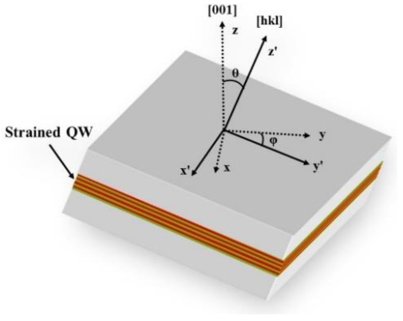
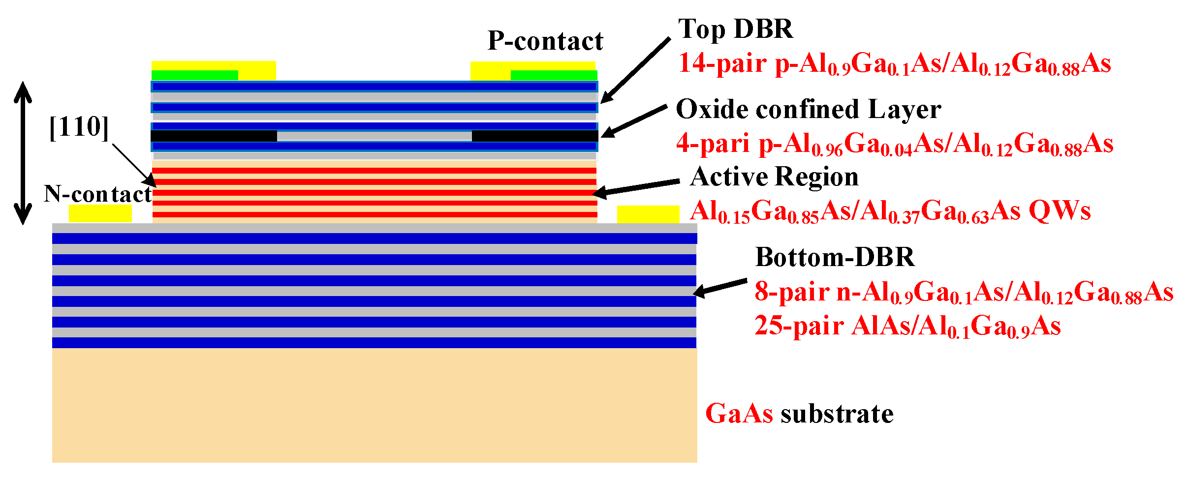
2. Materials and Methods
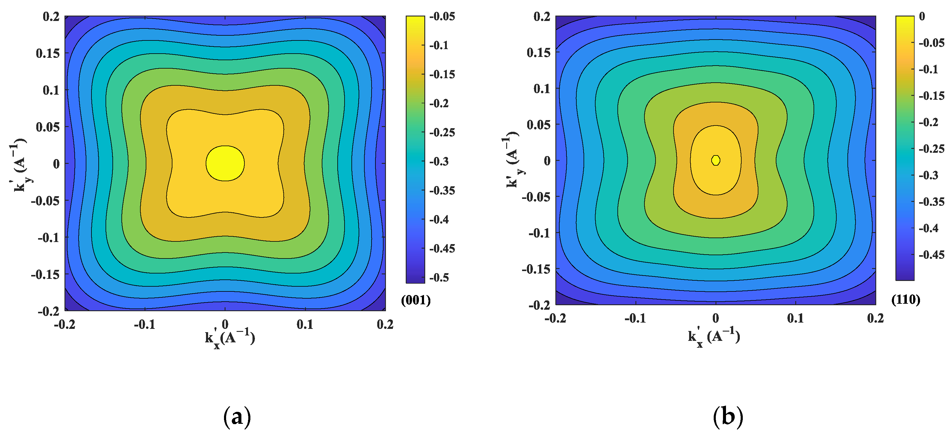
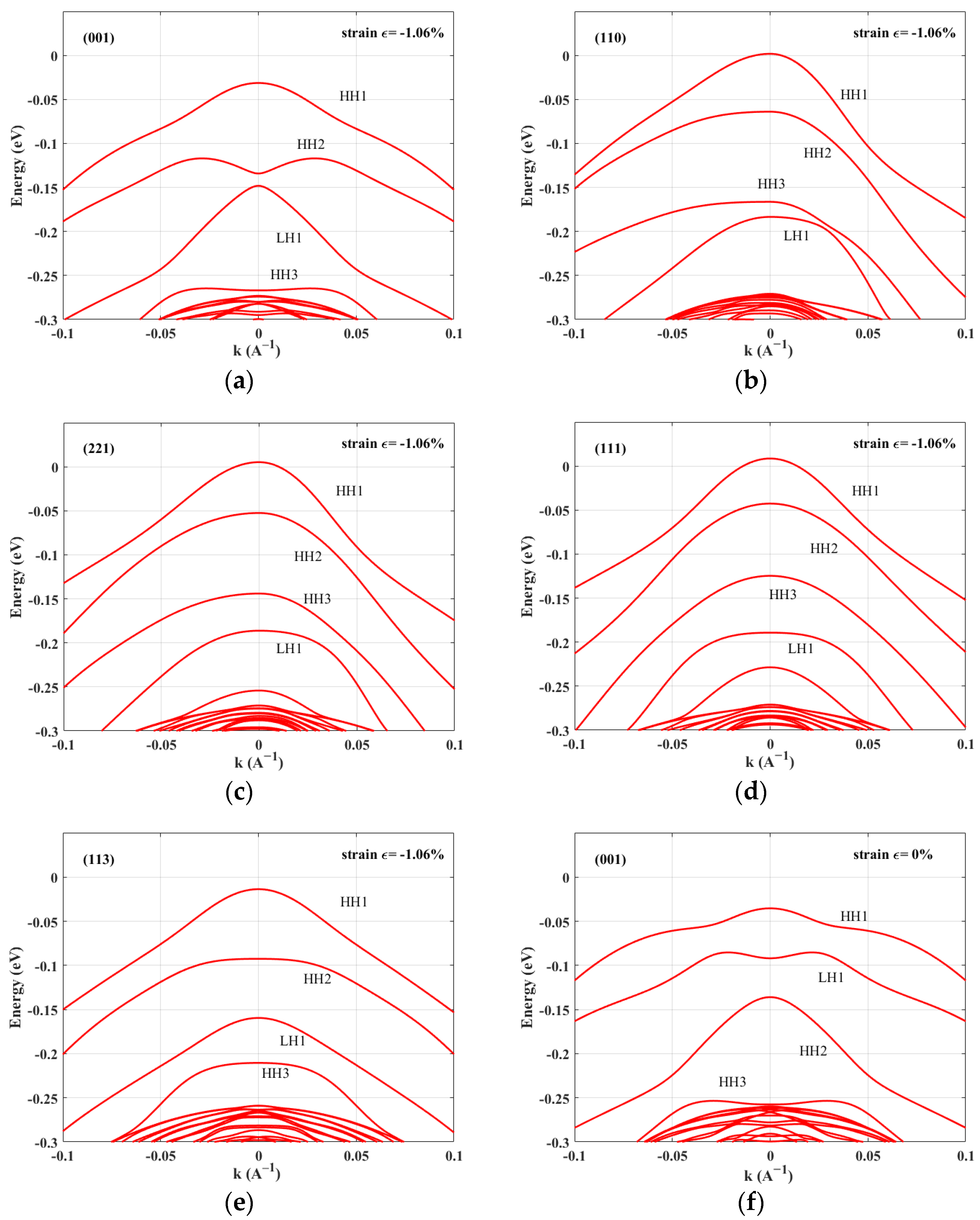
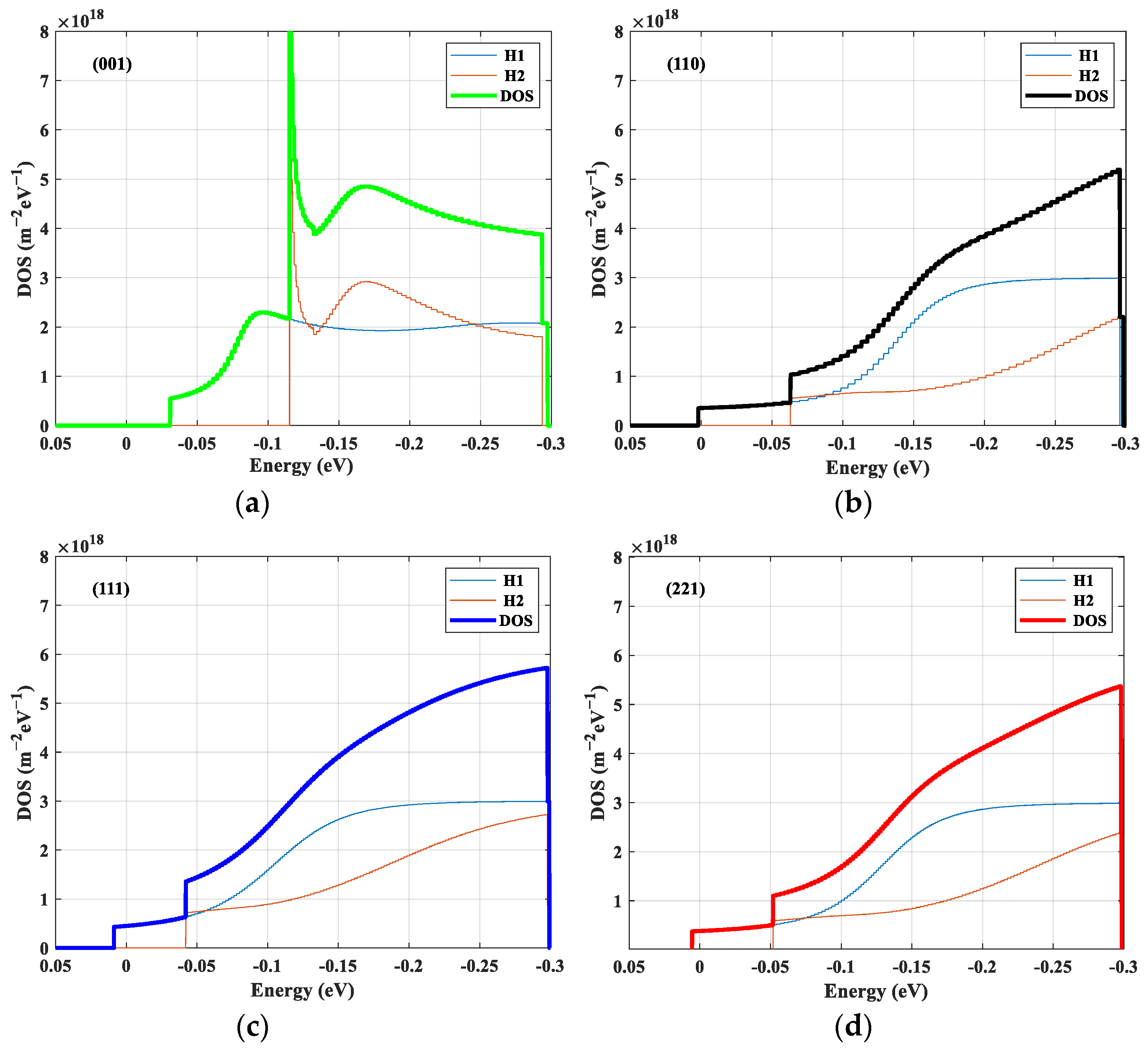
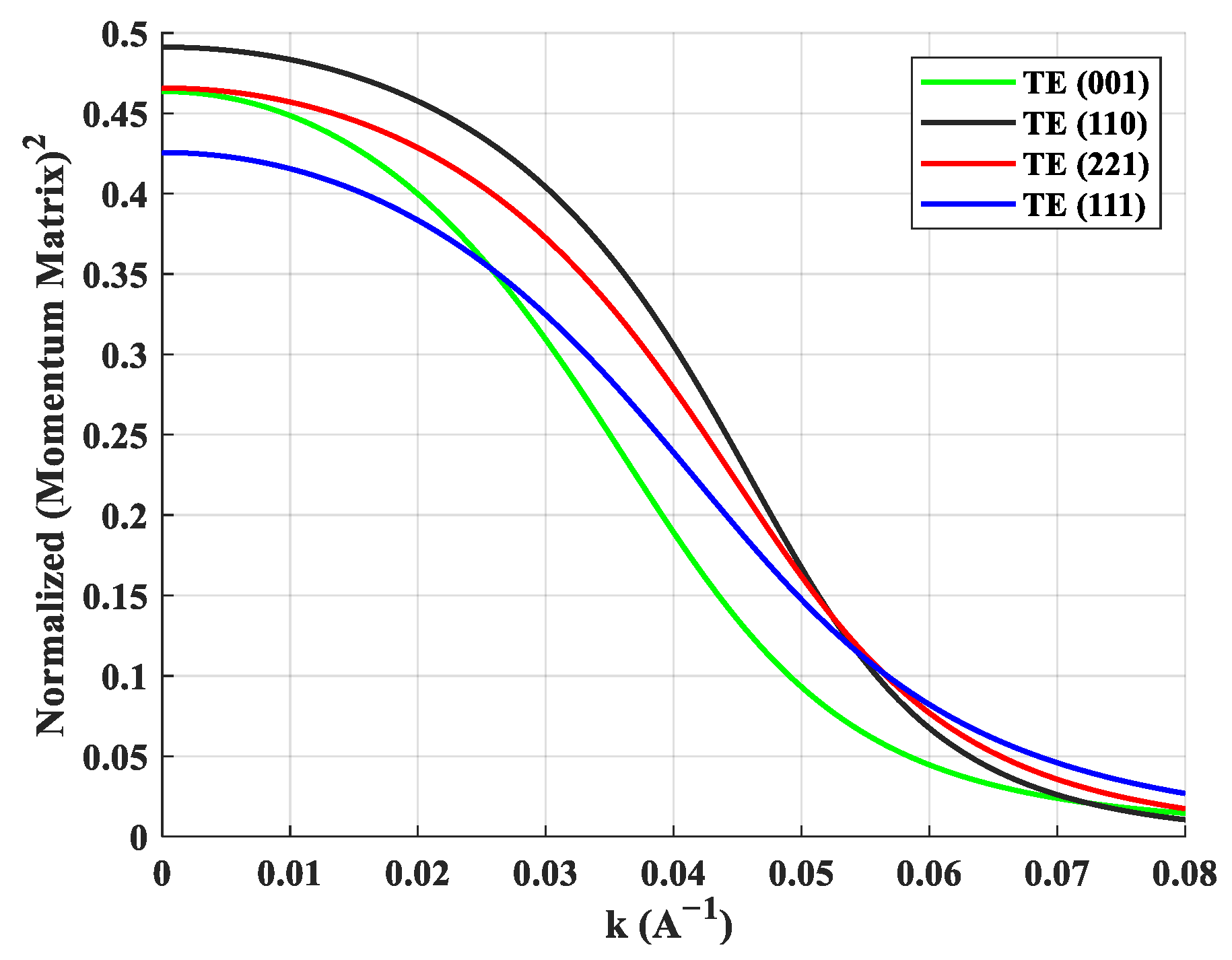
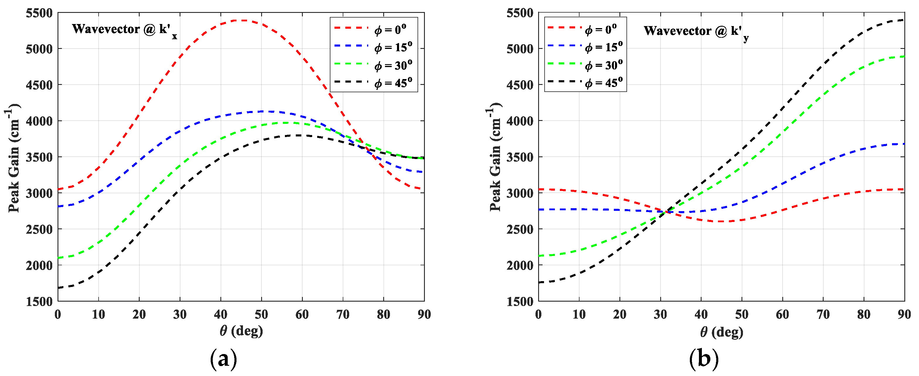
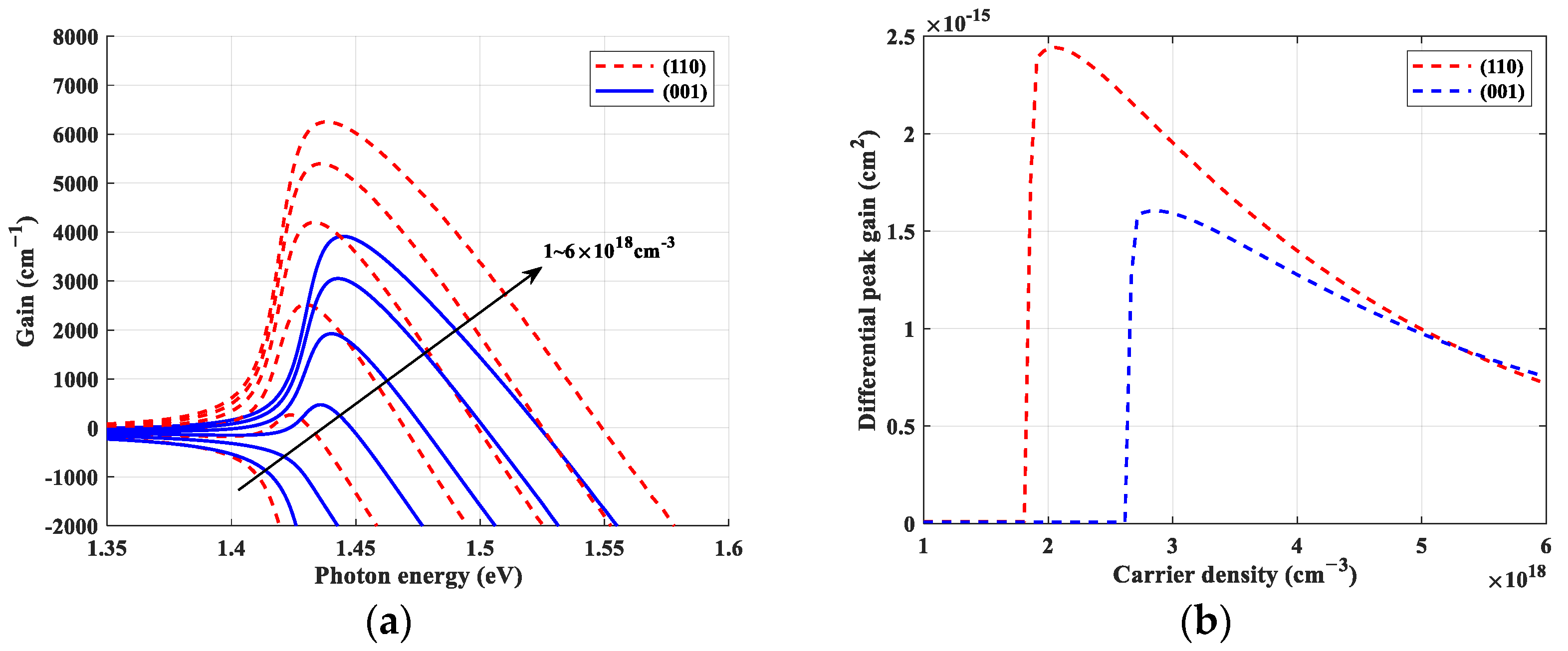
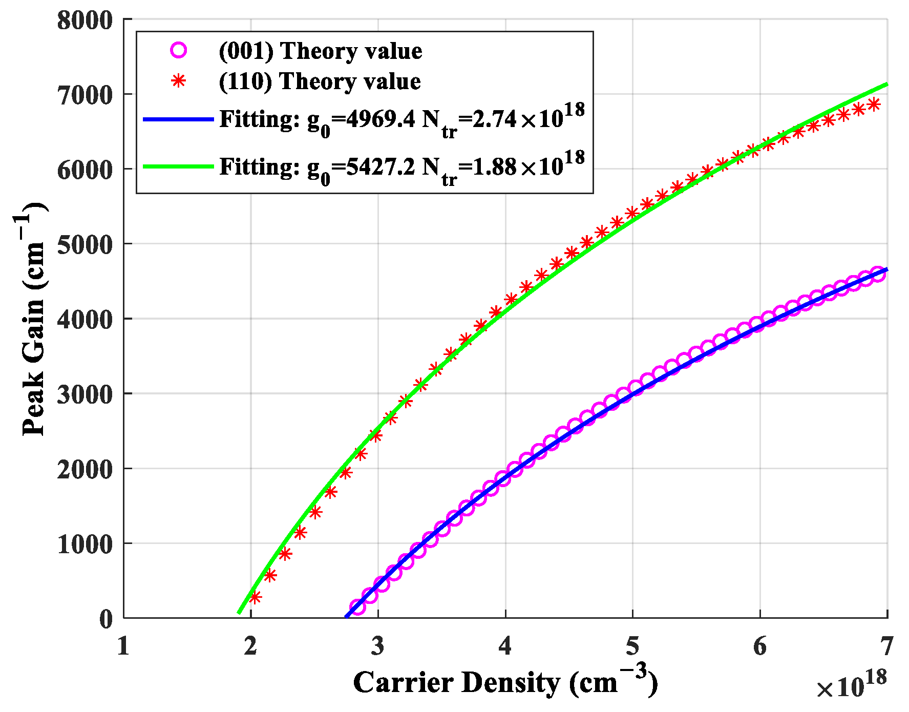
The effective Hamiltonian of a quantum well with an arbitrary crystal orientation can be obtained by rotating the (001) Hamiltonian. The Luttinger–Kohn 4 × 4 Hamiltonian is given by [30]:
H ( 001 ) = [ P + Q S R 0 S P Q 0 S R 0 P Q S 0 R S P + Q ]
Here, the matrix elements P = P + P ε , Q = Q + Q ε , R = R + R ε , S = S + S ε , P ε , Q ε , R ε , S ε are the contribution of strain.
P = 2 γ 1 2 m 0 ( k x 2 + k y 2 + k z 2 ) Q = 2 γ 2 2 m 0 ( k x 2 + k y 2 - 2 k z 2 ) R = 2 2 m 0 [ 3 γ 2 ( k x 2 k y 2 ) + i 2 3 k x k y ] S = 2 γ 3 2 m 0 3 ( k x i k y ) k z
P ε = a v ( ε x x + ε y y + ε z z ) Q ε = b 2 ( ε x x + ε y y 2 ε z z ) R ε = 3 2 b ( ε x x ε y y ) 3 i d ε x y S ε = - 3 d ( ε x z i ε y z )
Here, k x , k y and k z are the wave vectors in (001) crystal orientation, γ 1 , γ 2 and γ 3 are the Luttinger parameters; a v is the valence band deformation potential; ε i j ( i , j = x , y , z ) is the strain components; b and d are the band shear deformation potential. The Hamiltonian for QW with ( h k l ) orientation is obtained by [18]:
H ( h k l ) = R y ( θ ) R z ( φ ) H ( 001 ) R z ( φ ) R y ( θ )
where R y ( θ ) and R z ( φ ) denote the spinor rotations (see Appendix A for details), which converts the basis states from ( x , y , z ) coordinates to ( x , y , z ) coordinates. The angles θ and φ are the polar and azimuthal angles relative to the ( x , y , z ) coordinate system as shown in Figure 1.
The relationship between the coordinate systems for wave vectors and tensors is expressed as:
k i = α U i α k α ε i j = α , β U i α U j β ε α β C i j k l = α , β , γ , δ U i α U j β U k γ U l δ C α β γ δ
The following formula calculates the rotation matrix U [18]:
U = ( cos θ cos φ cos θ sin φ sin θ sin φ cos φ 0 sin θ cos φ sin θ sin φ cos θ )
φ = arctan ( h 2 + k 2 / l ) , θ = arctan ( k / h )
The strain components ε i j for the (hkl)-oriented strained QW are obtained by the coordinate transformation method [20] (see Appendix A for details). In 2D semiconductors, such as a QW structure, k z is considered as a pseudo-differential operator ( k z i z ) . Finally, the effective mass equation for a QW in (hkl) orientation is written as:
[ H ( h k l ) ( k z = i z ) + V h ( z ) I ^ ] ψ h ( z ) = E ψ h ( z )
For the conduction band, since the effective mass of the electron is almost isotropic in the quantum well plane, independent of the crystal orientation, it can be calculated using the parabolic band model [12,31].
The optical gain spectra of quantum well architecture with the valence band intermixing effect being considered is calculated using the following expression [11]:
g ( ω ) = 2 q 2 π n r c ε 0 m 0 2 ω L z n , m | M n , m | 2 × ( f c n ( k t ) f v m ( k t ) ) ( γ / π ) ( E n c ( k t ) E m v ( k t ) ω ) 2 + γ 2 k t d k t 2 π
f c ( k t ) = { 1 + exp [ E n c ( k t ) F c k B T ] } 1 f v ( k t ) = { 1 + exp [ E m v ( k t ) F v k B T ] } 1
where q is the elementary charge; c and ε 0 are the speed of light in free space and permittivity in free space; L z is the quantum well width; n r is the refractive index; f c n and f v n are Fermi–Dirac distribution functions. The electron and hole densities in the quantum well region are equal for non-doped quantum wells, which determines the quasi-Fermi energy levels in the conduction and valence bands. The intraband relaxation time γ 1 is assumed to be 0.1 ps. | M n , m | is the momentum matrix element for transitions M n , m = ψ n , k t c | p ^ | ψ m , k t v between ψ n , k t c and ψ m , k t v where p ^ is the momentum operator. The k-selection rule is observed.

3. Results

In this section, the crystal orientation-dependent optical properties for In0.15Ga0.85As/Al0.37Ga0.63As strained QW with L z = 4 nm are calculated. The biaxial compressive strain considered is ε x x = 1.06 % and is due to the lattice mismatch between the well and the substrate. Figure 2 shows the calculated equal-energy patterns of the first valence band (HH1) in the k x k y plane for a strained QW with the (001), (110), (111), and (221) orientations, respectively. k x and k y represent the in-plane wave vectors. The material parameters are shown in Table 1. The alloy properties of In0.15Ga0.85As are obtained by linear interpolation, except for the gap energy:
E g ( A l x G a 1 x A s ) = 1.424 + 1.27 x P ( A l x G a 1 x A s ) = x P ( A l A s ) + ( 1 - x ) P ( G a A s ) E g ( I n 1 x G a x A s ) = 0.324 + 0.7 x + 0.4 x 2 P ( I n 1 x G a x A s ) = x P ( G a A s ) + ( 1 - x ) P ( I n A s )
The anisotropic effect of the valence band in each orientation is seen. The symmetry of the valence band for QWs with (111) orientation is C 6 rotation symmetry and for (001) cases is the C 4 rotation symmetry. Compared to the (001) and (111) crystal orientations, (110) and (221) orientations have lower twofold symmetry, which predicts that the gain is anisotropic in the QW plane.
In Figure 3, the valence sub-band dispersions as a function of the in-plane wave vectors k x and k y for the orientations of (001), (111), (110), (221), (113), and (001) unstrained QWs are calculated. The H H i and L H i represent the heavy hole band and light hole band, and i denotes the sub-band level. They can be distinguished by the dominant component of the wave function in the Brillouin-zone center (k = 0). As noticed in Figure 3, the result for the (001) orientation unstrained QW exhibits non-parabolicity with minimal heavy and light hole splitting. With strain considered in the QW, the splitting between the HH1 and the LH1 is enhanced by pushing the LH1 band away from the QW. The valence band distribution of the strained QW in (113) orientation is the same as that in (001) orientation. However, the energy spacing between HH2 and LH1 in (113) orientation is about 66.95 meV, which is much larger than that of 14.1 meV in (001) orientation. On the other hand, the valence sub-band dispersions of (110) and (221) oriented QWs are anisotropic in the QW plane, and the effective mass of the topmost valence sub-band becomes light in the direction of k y . This is unlike the (111) orientation in which the characteristics of the sub-band dispersion is hexagonally symmetrical in-plane k x k y . The splitting of the sub-bands in the (110) and (221) orientation further separate the HH and LH sub-bands, and the valence-band mixing effect is reduced in the QW plane, resulting in the reduction of the density of states near the band edges, especially for the [ 1 ¯ 10 ] direction in the (110) orientation QW plane. Thus, the optical gain and differential gain of InGaAs/AlGaAs lasers along (110) and (221) growth planes are expected to be superior to the conventional (001) crystal orientation.
The density of states (DOS) is important for understanding the carrier occupation in a QW. Figure 4 shows the density of states for the first two sub-bands of each crystal-oriented valence band structure in Figure 3. DOS presents a step-like shape for the four orientations. For the (001) crystal orientation, the increase in DOS values as a function of energy is suppressed to a degree due to the enlarged splitting energy between the valence sub-bands. However, at about 60 meV below the band edge, DOS already has a value more than four times larger than the value at the band edge. On the other hand, the (110), (111), and (221) crystal-oriented quantum wells’ density of states are less than 2 × 10¹⁸ m−2eV−1 in the energy range of 130 meV, 91 meV, and 120 meV, respectively. The reduction of the density of states near the band edge of the valence band will reduce the carrier density per unit area required to achieve transparency, and also reduce the effect of improving the differential gain of the quantum well structure.
The selection rules indicate that the inter-band transition only occurs from the first-conduction sub-band (C1) to the first HH sub-band (HH1) and to the first LH sub-band (LH1) at the Brillouin zone center. Using this information and Figure 3, we can see that the transition is mainly caused from C1 to HH1, therefore, we mainly consider the transverse electric (TE) polarization state of the transition from C1 to HH1. Figure 5 calculates the values of the optical matrix elements between C1 and HH1 for different crystal orientations, and the results show that the (110) orientation has the largest value of the optical matrix element due to the largest overlap integral of the conduction band and valence band wave functions, followed by the (221) crystal orientation. The value of the optical matrix element in the (001) crystal direction at k = 0 is larger than that in the (111) crystal orientation, but the value in the (001) orientation decreases rapidly with the increase of the k-wave vector.
As shown in Figure 6a,b, we calculated the peak material gain along the orthogonal plane wave vectors with an arbitrary crystal orientation. The carrier concentration is n = 5 × 1018 cm−3. It is noted that the peak gain in the (001) orientation is dependent on the azimuthal angles, which is the smallest in the ( 11 ) ( φ = π / 4 , θ = 0 ) orientation. The results for the (110) ( φ = π / 4 , θ = π / 2 ) and equivalent (101) ( φ = 0 , θ = π / 4 ) orientations show that the largest anisotropic gain is in the k x and k y direction. On the other hand, the QW peak gain of the (001) ( φ = 0 , θ = 0 ) and (111) ( φ = π / 4 , θ 54 . 7175 o ) orientations is isotropic in the k x and k y direction due to the high rotational symmetry of the valence band. The QWs with (221) and (110) crystal orientation show superior performance compared to the conventional (001) oriented QW structure, but the maximum peak gain is observed along the [ 1 ¯ 10 ] ( k y ) direction in the (110) orientation or [ 10 1 ¯ ] ( k x ) direction in (101) orientation, which is about 1.76 times that of the conventional (001) crystal orientation due to the anisotropic energy dispersion of the top valence sub-band and the increase of the optical matrix element. Therefore, we choose the (110) crystal orientation for the remainder of the presented analysis.
The TE polarization gain spectra and quantum well differential gain as a function of carrier concentration for (001) and (110) crystal orientations are shown in Figure 7a,b. The results reveal that the (110) crystal orientation has high gain characteristics at the same carrier concentration injection. Furthermore, it is observed from Figure 7b that the transparent carrier concentration in the (110) crystal orientation decreases significantly due to a lower density of states near the band edge. The maximum differential gain in the (110) orientation is 2.454 × 10⁻¹⁵ cm2 for a carrier density of 1.88 × 1018 cm−3, which is approximately 1.52 times that of the (001) crystal direction. QWs with a (110) crystal orientation VCSELs can achieve higher speed modulations.

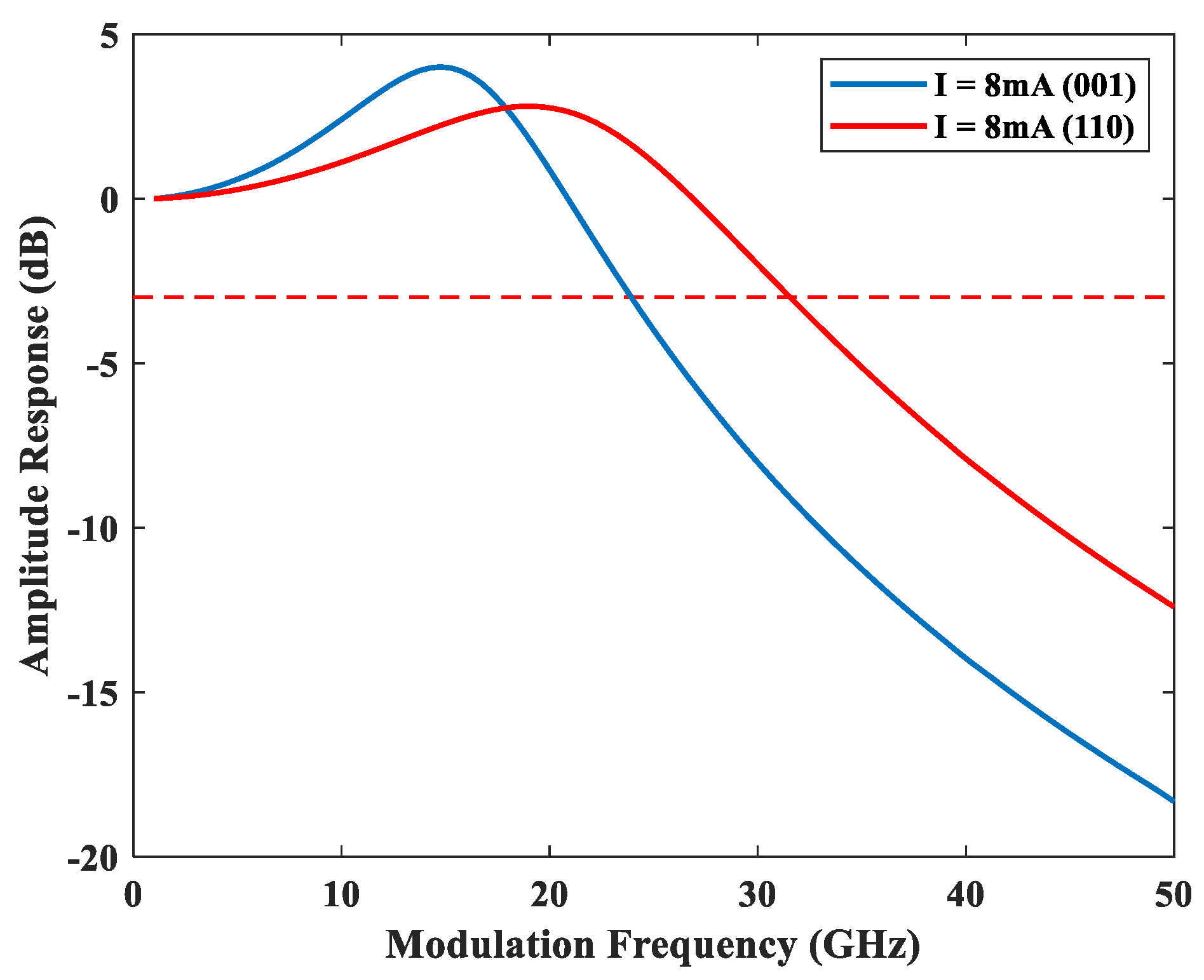
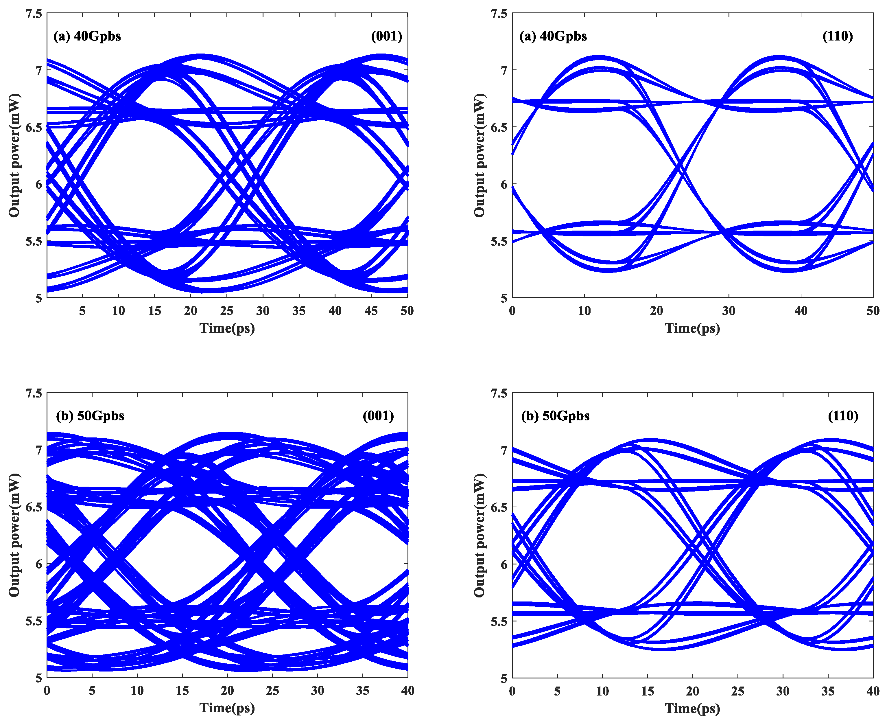
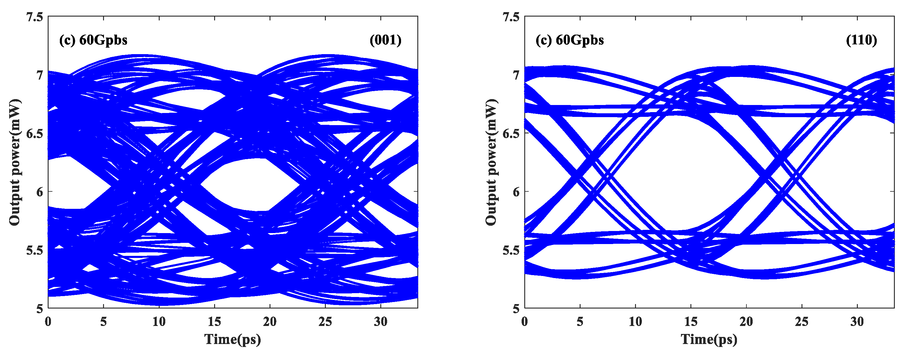
4. Modulation Response and High-Speed Modulation

The modulation characteristics of high-speed oxide confined 850 nm VCSEL devices with quantum wells grown in (110) and (001) crystal orientations is typically modeled by the single-mode VCSEL rate equation using the fourth-order Runge-Kutta algorithm:
d N ( t ) d t = η i I ( t ) q V N ( t ) τ n v g g S ( t ) 1 + ε S ( t ) d S ( t ) d t = Γ v g g S ( t ) 1 + ε S ( t ) S ( t ) τ p + Γ β N ( t ) τ n
where I , v g , V , ε , Γ , q , g , β , τ p and τ n are the bias current, the group velocity of propagated light, elementary charge, active section volume, gain saturation coefficient, optical confinement factor, material gain, spontaneous emission factor, photon lifetime, and carrier lifetime, respectively. Typical values of the parameters used in the simulation are shown in Table 2. The VCSEL cavity is described in Figure 8. Typically, as in our example, the barrier width in the active region is thick enough, and the quantum wells are uncoupled from each other [33], so it is reasonable to use the single quantum well model for the whole structure. The general empirical expression between the material gain g and carrier density N in quantum well lasers is [34]:
g = g 0 log ( N N t r )
where g 0 is the material gain coefficient, N t r is transparency carrier density. Figure 9 shows the results of the gain versus carrier density curve fitting of the logarithmic function in (001) and (110) orientations, from which it can see that the numerical results are in great agreement with Equation (13). The calculated transparency carrier density obtained by logarithmic fitting decreases from 2.74 × 1018 cm−3 to 1.88 × 1018 cm−3 and the gain coefficient increases from 4969.4 cm−1 to 5427.2 cm−1 in the (110) orientation compared to the conventional (001) orientation.
As shown in Figure 10, the small-signal modulation response of the two crystal-oriented VCSELs is calculated by inserting the material gain coefficient g 0 , the transparent carrier concentration N t r , and the other parameters in Table 2 into the rate equation. It is found that when the injection current is 8 mA, the 3 dB response bandwidth in the (001) orientation is 24.25 GHz, while the 3 dB response bandwidth in the (110) orientation is about 32.3 GHz, which is about 1.33 times higher compared to the (001) crystal orientation.
Figure 11 shows the large-signal eye diagram of the two crystal-oriented VCSELs at 8 mA for different transmission data rates of 40 Gbps, 50 Gbps, and 60 Gbps. Comparing the eye diagrams of Figure 11a,b, the quality of the eye diagram in the (110) orientation is significantly better than that in the (001) crystal orientation at the transmission data rates of 40 Gbps and 50 Gbps. As noticed in Figure 11c, the eye diagram in the (001) crystal orientation is severely degraded at the transmission data rate of 60 Gbps, while that in the (110) crystal orientation can be maintained in partially open condition.

5. Conclusions

A numerical investigation of strained InGaAs/AlGaAs quantum well VCSELs emitting at around 850 nm has been studied. The key optoelectronic properties of the unconventional crystal orientation were analyzed in detail to demonstrate its superiority over the conventional (001) crystal growth orientation. It is shown that the maximum peak gain is obtained in the (110) orientation with the transparent carrier concentration decreasing from 2.74 × 1018 cm−3 to 1.88 × 1018 cm−3 compared with the (001) orientation due to the reduction of the density of states. The (110) orientation offers the highest optical matrix element value due to the major overlap integral of the conduction and valence band wave functions and significant gain characteristics, enabling high-speed modulation. As a result, it contributes to optimizing the quantum well structure’s differential gain. The small-signal and large-signal modulation characteristics of VCSELs are numerically simulated by solving the rate equation based on the fourth-order Runge–Kutta method. The 3 dB modulation bandwidth in the (110) orientation is 1.33 times higher than that in the (001) orientation, and excellent modulation rates up to 60 Gbps are obtained numerically. Thus, the (110)-oriented InGaAs/AlGaAs quantum well VCSEL is promising for high-speed and high-performance near-infrared optoelectronic applications.

Author Contributions

Conceptualization, J.Z. and J.L.; methodology, J.L.; software, J.L.; validation, J.Z. and F.G.; formal analysis, J.L.; supervision, J.Z. and F.G.; Visualization, J.Z., F.G.; writing—original draft preparation, J.L.; writing—review and editing, J.Z. and F.G.; funding acquisition, J.Z. All authors have read and agreed to the published version of the manuscript.

Funding

This research was funded by the National Key Technology R&D Program (grant number. 2018YFA0209001).

Conflicts of Interest

The authors declare no conflict of interest.

Appendix A

The spinor rotations matrices that transform the valence band Hamiltonian from a (001) orientation to an arbitrary crystal orientation are the following [18]:
R y ( θ ) = [ α 3 - 3 α 2 β 3 α β 2 β 3 3 α 2 β α 3 - 2 α β 2 2 α 2 β + β 3 3 α β 2 3 α β 2 2 α 2 β β 3 α 3 - 2 α β 2 - 3 α 2 β β 3 3 α β 2 3 α 2 β α 3 ]
R z ( φ ) = [ e i ( 3 / 2 ) φ 0 0 0 0 e i ( 1 / 2 ) φ 0 0 0 0 e i ( 1 / 2 ) φ 0 0 0 0 e i ( 3 / 2 ) φ ]
Here, α = cos ( θ / 2 ) , β = sin ( θ / 2 ) .
The strain components for the (hkl)-oriented strained QW under uniform biaxial stress are obtained by the coordinate transformation method. The plane strain tensor components in the ( x , y , z ) coordinate system are known as:
ε x x = ε y y = a b a w a w
There is no in-plane shear strain in the film, thus ε x y = ε y x = 0 , and the other independent strain tensor components ε x z , ε y z , ε z z can be obtained by Hooke’s law:
T α β + C α β i j ε i j = 0
For α , β = 1, 2, 3, i , j = x, y. where C α β i j is the matrix elements of the stiffness matrix, T α β is the stress applied to the film. The substrate applied a uniform in-plane stress to the film, thus T 33 = T 23 = T 13 = 0 . According to Hooke’s law, the following formula is obtained [29]:
i , j C 33 i j ε i j = 0 , i , j C 23 i j ε i j = 0 , i , j C 13 i j ε i j = 0
The strain components ε x x , ε y y , ε x y , ε y x are known, using the symmetry of C α β i j and ε i j , therefore, a matrix equation for the three independent strain tensor components ε x z , ε y z , ε z z can be written as:
( C 3333 C 3323 C 3331 C 2333 C 2323 C 2331 C 3133 C 3123 C 3131 ) [ ε z z / 2 ε y z ε x z ] = - ε | | 2 [ C 3311 + C 3322 C 2311 + C 2322 C 3111 + C 3122 ]
The C α β i j parameters can be obtained by Equation (A5). Finally, all strain components ε i j for the (hkl)-oriented strained QW under uniform biaxial stress are obtained.

References

  1. Iga, K. Forty years of vertical-cavity surface-emitting laser: Invention and innovation. Jpn. J. Appl. Phys. 2018, 57, 08PA01. [Google Scholar] [CrossRef]
  2. Cheng, H.-T.; Yang, Y.-C.; Liu, T.-H.; Wu, C.-H. Recent advances in 850 nm VCSELs for high-speed interconnects. Proc. Photonics 2022, 9, 107. [Google Scholar] [CrossRef]
  3. Liu, A.; Wolf, P.; Lott, J.A.; Bimberg, D. Vertical-cavity surface-emitting lasers for data communication and sensing. Photonics Res. 2019, 7, 121–136. [Google Scholar] [CrossRef]
  4. Johnson, R.H.; Kuchta, D.M. 30 Gb/s directly modulated 850 nm datacom VCSELs. In Proceedings of the Conference on Lasers and Electro-Optics, San Jose, CA, USA, 4–9 May 2008; Optica Publishing Group: California, CA, USA, 2008. [Google Scholar]
  5. Healy, S.B.; O’Reilly, E.P.; Gustavsson, J.S.; Westbergh, P.; Haglund, Å.; Larsson, A.; Joel, A. Active region design for high-speed 850-nm VCSELs. IEEE J. Quantum Electron. 2010, 46, 506–512. [Google Scholar] [CrossRef]
  6. Haglund, E.; Westbergh, P.; Gustavsson, J.S.; Haglund, E.P.; Larsson, A.; Geen, M.; Joel, A. 30 GHz bandwidth 850 nm VCSEL with sub-100 fJ/bit energy dissipation at 25–50 Gbit/s. Electron. Lett. 2015, 51, 1096–1098. [Google Scholar] [CrossRef] [Green Version]
  7. Yang, Y.-C.; Cheng, H.-T.; Wu, C.-H. 30 GHz Highly Damped Oxide Confined Vertical-Cavity Surface-Emitting Laser. In Proceedings of the 2021 IEEE Photonics Conference (IPC), Online, 18–21 October 2021. [Google Scholar]
  8. Wang, H.-L.; Fu, W.; Qiu, J.; Feng, M. 850 nm VCSELs for 50 Gb/s NRZ Error-Free Transmission over 100-m OM4 and up to 115 C Operation. In Proceedings of the Optical Fiber Communication Conference, San Jose, CA, USA, 3–7 March 2019. (USA)Optical Society of America. [Google Scholar]
  9. Huang, C.-Y.; Wang, H.-Y.; Peng, C.-Y.; Tsai, C.-T.; Wu, C.-H.; Lin, G.-R. Multimode VCSEL enables 42-GBaud PAM-4 and 35-GBaud 16-QAM OFDM for 100-m OM5 MMF data link. IEEE Access 2020, 8, 36963–36973. [Google Scholar] [CrossRef]
  10. Westbergh, P.; Gustavsson, J.S.; Haglund, A.; Skold, M.; Joel, A.; Larsson, A. High-Speed, Low-Current-Density 850 nm VCSELs. IEEE J. Sel. Top. Quantum Electron. 2010, 46, 506–512. [Google Scholar] [CrossRef]
  11. Chuang, S.L. Physics of Photonic Devices; John Wiley & Sons: Hoboken, NJ, USA, 2012. [Google Scholar]
  12. Roy, S.; Al-tabatabai, K.F.; Chakraborty, A.; Kabir, M.A.; Hossain, M.S.; Abdulrazak, L.F.; Howlader, A.H.; Islam, M.R.; Hossain, M.B. Numerical investigation into optical and electronic performance of crystal orientation-dependent InGaAs/InP near-infrared laser. Results Phys. 2021, 26, 104353. [Google Scholar] [CrossRef]
  13. Roy, S.; Kabir, M.I.; Al-Mamun, K.A. Optoelectronic performance of vertical cavity surface emitting InGaAs/InP QW lASER in non-conventional orientation. In Proceedings of the 2016 International Conference on Innovations in Science, Engineering and Technology (ICISET), Dhaka, Bangladesh, 28–29 October 2016; IEEE: New York, NY, USA, 2017. [Google Scholar]
  14. Hasan, M.; Islam, M.; Teramoto, K. Crystallographic orientation-dependent optical properties of GaInSb mid-infrared quantum well laser. Optik 2012, 123, 1993–1997. [Google Scholar] [CrossRef]
  15. Ismaeel, M.M.; Mijwil, M.M. Optical and Electrical Performance Analysis of InGaAs/InP Laser for Various Crystal Orientations. Asian J. Eng. Technol. 2022, 10. [Google Scholar] [CrossRef]
  16. Saidi, H.; Zitouni, O.; Ridene, S. Investigation of orientation dependence of piezoelectric effects in strained GaAs/InGaAs quantum well laser. Mater. Sci. Eng. B 2021, 273, 115400. [Google Scholar] [CrossRef]
  17. Saidi, H.; Msahli, M.; Dhafer, R.B.; Ridene, S. Self-consistent optimization of [111]-algainas/inp mqws structures lasing at 1.55 μm by a genetic algorithm. Superlattices Microstruct. 2017, 112, 200–209. [Google Scholar] [CrossRef]
  18. Niwa, A.; Ohtoshi, T.; Kuroda, T. Orientation dependence of optical properties in long wavelength strained quantum-well lasers. IEEE J. Sel. Top. Quantum Electron. 1995, 1, 211–217. [Google Scholar] [CrossRef]
  19. Ohtoshi, T.; Takahashi, M. Band Engineering of the Polarization and Gain Properties in VCSELs. In Vertical-Cavity Surface-Emitting Laser Devices; Springer: Berlin/Heidelberg, Germany, 2003; pp. 99–134. [Google Scholar]
  20. Hinckley, J.; Singh, J. Influence of substrate composition and crystallographic orientation on the band structure of pseudomorphic Si-Ge alloy films. Phys. Rev. B 1990, 42, 3546. [Google Scholar] [CrossRef] [PubMed]
  21. Yoo, K.; Albrecht, J.; Ram-Mohan, L. Strain in layered zinc blende and wurtzite semiconductor structures grown along arbitrary crystallographic directions. Am. J. Phys. 2010, 78, 589–597. [Google Scholar] [CrossRef]
  22. Hong, W.-P.; Park, S.-H. Optical anisotropy in type-II (110)-oriented GaAsSb/GaAs quantum wells. Solid State Commun. 2020, 314, 113934. [Google Scholar] [CrossRef]
  23. Park, S. Optical anisotropy in (1 1 0)-oriented zinc-blende GaN/AlGaN quantum wells. Semicond. Sci. Technol. 2008, 23, 075047. [Google Scholar] [CrossRef]
  24. Ohtoshi, T.; Niwa, A.; Kuroda, T. Orientation dependence of optical gain in zincblende-GaN strained-quantum-well lasers. IEEE J. Sel. Top. Quantum Electron. 1998, 4, 527–530. [Google Scholar] [CrossRef]
  25. Duggen, L.; Willatzen, M.; Lassen, B. Crystal orientation effects on the piezoelectric field of strained zinc-blende quantum-well structures. Phys. Rev. B 2008, 78, 205323. [Google Scholar] [CrossRef]
  26. Roy, S.; Kiratnia, S.G.; Roy, P.N.; Hasan, M.M.; Howlader, A.H.; Rahman, M.S.; Islam, M.R.; Rana, M.M.; Abdulrazak, L.F.; Mehedi, I.M. Numerical investigation into optoelectronic performance of InGaN blue laser in polar, non-polar and semipolar crystal orientation. Crystals 2020, 10, 1033. [Google Scholar] [CrossRef]
  27. Sarker, M.S.; Islam, M.M.; Hasan, M.M.; Islam, M.R. Crystal orientation dependent performance of cubic InGaN QW blue-violet laser. In Proceedings of the 2015 18th International Conference on Computer and Information Technology (ICCIT), Dhaka, Bangladesh, 21–23 December 2015. [Google Scholar]
  28. Islam, M.M.; Sarker, S.; Hasan, M.; Islam, R. Orientation dependent performance of 635nm vertical cavity surface emitting QW red laser. In Proceedings of the 2015 2nd International Conference on Electrical Information and Communication Technologies (EICT), Piscataway, NJ, USA, 10–12 December 2015. [Google Scholar]
  29. Chang, G.-E.; Cheng, H.H. Optical gain of germanium infrared lasers on different crystal orientations. J. Phys. D Appl. Phys. 2013, 46, 065103. [Google Scholar] [CrossRef]
  30. Piprek, J. Semiconductor Optoelectronic Devices: Introduction to Physics and Simulation; Elsevier: Amsterdam, The Netherlands, 2013. [Google Scholar]
  31. Xia, J.-B. Effective-mass theory for superlattices grown on (11N)-oriented substrates. Phys. Rev. B 1991, 43, 9856. [Google Scholar] [CrossRef]
  32. Vurgaftman, I.; Meyer, J.R.; Ram-Mohan, L.R. Band parameters for III–V compound semiconductors and their alloys. J. Appl. Phys. 2001, 89, 5815–5875. [Google Scholar] [CrossRef] [Green Version]
  33. Bandelow, U.; Hunlich, R.; Koprucki, T. Simulation of static and dynamic properties of edge-emitting multiple-quantum-well lasers. IEEE J. Sel. Top. Quantum Electron. 2003, 9, 798–806. [Google Scholar] [CrossRef]
  34. Coldren, L.A.; Corzine, S.W.; Mashanovitch, M.L. Diode Lasers and Photonic Integrated Circuits; John Wiley & Sons: Hoboken, NJ, USA, 2012. [Google Scholar]
Figure 1. Crystallographic coordinate system ( x , y , z ) and the coordinate system ( x , y , z ) for a (hkl)-oriented strained QW.
Crystals 12 01459 g001
Figure 2. Equal-energy contour plots of the first valence band (HH1) in strain InGaAs QW with (a) (001), (b) (110), (c) (111), and (d) (221) orientations. The unit of the energy level in the legend is eV.
Crystals 12 01459 g002aCrystals 12 01459 g002b
Figure 3. Valence band dispersions for a 1.06% compressive strained InGaAs QW with (a) (001), (b) (110), (c) (221), (d) (111), and (e) (113) orientations, and (f) for an unstrained InGaAs QW with (001) orientation.
Crystals 12 01459 g003
Figure 4. DOS for 1.06% compressive strained InGaAs QW structures with (a) (001), (b) (110), (c) (111), and (d) (221) orientations.
Crystals 12 01459 g004
Figure 5. Crystal orientation–dependent normalized momentum matrix element square for the C1–HH1 transition.
Crystals 12 01459 g005
Figure 6. Plots of the material gain in strained InGaAs QW along the orthogonal plane wave vectors (a) k x and (b) k y with arbitrary crystal orientations.
Crystals 12 01459 g006
Figure 7. Calculated (a) gain spectra and (b) differential gain for (001) and (110)-oriented strained QW lasers.
Crystals 12 01459 g007
Figure 8. Schematic cross-section of InGaAs 850 nm VCSEL structure.
Crystals 12 01459 g008
Figure 9. Gain versus carrier density curve fits for (001) and (110) crystal orientations in strain InGaAs QW.
Crystals 12 01459 g009
Figure 10. Small signal frequency response for (001) and (110) crystal orientations VCSELs.
Crystals 12 01459 g010
Figure 11. Eye diagrams of (001) and (110) crystal orientations VCSELs for different data rates of (a) 40 Gbps, (b) 50 Gbps and (c) 60 Gbps.
Crystals 12 01459 g011aCrystals 12 01459 g011b
Table 1. Material parameters used in the calculation. Adapted with permission from [18,32].
SymbolQuantity (Unit)GaAsInAsAlAs
α Lattice constant ( Å ) 5.65336.05845.6600
E g ( e V ) Energy parameter1.4240.3543.03
m e / m 0 Conduction-band effective-masses0.0670.0230.15
γ 1 Luttinger parameters6.8519.673.45
γ 2 2.18.370.68
γ 3 2.99.291.29
α c Deformation potentials (eV)−7.17−5.08−5.64
α v 2.72.52.6
b −1.7−1.8−1.5
d −4.55−3.6−3.4
C 11 Elastic stiffness constants ( 10 11   d y n / c m 2 ) 11.888.32912.02
C 22 5.384.5625.70
C 44 5.943.9595.89
Table 2. Parameters used in the simulation of VCSEL. Adapted with permission from [5].
SymbolQuantityValue
η i Current injection efficiency0.9
V Active region volume2.262 × 10−12 cm3
v g Group velocity8.53 × 109 cm s−1
τ n Carrier lifetime2 ns
Γ Confinement factor0.0289
α i n Internal loss10 cm−1
L e f f Effective cavity length1 μm
R 1 The reflectivity of bottom DBR99.9%
R 2 The reflectivity of top DBR99.7%
β Spontaneous emission factor0.5 × 10−5
ε Gain compression factor0.5 × 10−18 cm−3
Publisher’s Note: MDPI stays neutral with regard to jurisdictional claims in published maps and institutional affiliations.

