Article

Enhanced Thermoelectric Performance of ZnO-Based Thin Films via Interface Engineering

State Key Laboratory of New Ceramics and Fine Processing, School of Materials Science and Engineering, Tsinghua University, Beijing 100084, China
*
Author to whom correspondence should be addressed.
Crystals 2022, 12(10), 1351; https://doi.org/10.3390/cryst12101351
Submission received: 31 August 2022 / Revised: 16 September 2022 / Accepted: 22 September 2022 / Published: 24 September 2022
(This article belongs to the Special Issue Advances in Thermoelectric Thin Films)

Abstract

:
Zinc oxide (ZnO) is a potential thermoelectric material with good chemical and thermal stability as well as an excellent Seebeck coefficient. However, the extremely low carrier concentration brings poor electrical transport properties. Although Gallium (Ga) doping could increase the carrier concentration of ZnO film, its thermoelectric performance is still limited due to the deteriorated Seebeck coefficient and enhanced thermal conductivity. Interface engineering is an effective strategy to decouple electron-phonon interaction for thermoelectric materials. Thus, in this work, GZO (Ga-doped ZnO)/NAZO (Ni, Al co-doped ZnO) multilayer films were designed to further improve the thermoelectric properties of GZO films. It was found that GZO/NAZO multilayer films possessed better electrical conductivity, which was attributed to the increased carrier concentration and Hall mobility. Meanwhile, benefiting from the energy filtering that occurred at GZO/NAZO interfaces, the density of states effective mass increased, resulting in comparable Seebeck coefficient values. Ultimately, an enhanced power factor value of 313 μW m−1 K−2 was achieved in the GZO/NAZO multilayer film, which is almost 46% larger than that of GZO film. This work provides a paradigm to optimize the thermoelectric performance of oxide films and other thermoelectric systems by multilayer structure design with coherent interfaces.

1. Introduction

Thermoelectric materials can realize direct conversion between heat and electricity via the Seebeck and Peltier effects, which is suitable for power generation and precise cooling [1,2,3,4]. Advances in 5G communications and the integrated circuits industry promoted portable and wearable electronics, and there is an urgent need for self-powered energy and chip cooling technology [5,6]. In order to fulfill the requirement, thermoelectric thin films with lightweight, small size and controllable structures are developed [7]. An ideal thermoelectric material should have excellent electrical properties and low thermal conductivity, as the performance is related to a dimensionless figure of merit (ZT) and can be described as ZT = S2σT/κ. Here, S, σ, κ and T stand for the Seebeck coefficient, electrical conductivity, thermal conductivity and absolute temperature, respectively [8]. Compared to bulks, thin films usually have lower κ due to the lower dimension [9,10]. Thus, it is important to improve electrical transport properties for thin films, which is related to the power factor (PF = S2σ).
Zinc oxide (ZnO) thin films are a kind of potential thermoelectric materials due to their merits such as non-toxicity, low cost, outstanding chemical and thermal stability as well as high visible-light transparency [11]. However, intrinsic ZnO possesses relatively low σ, which originates from the extremely low carrier concentration (n) [12]. In order to solve this problem, elements such as Al, Ga, In, Sb and Sn were doped in the Zn site. Among the dopants, Al and Ga are much more effective in improving the electrical conductivity for ZnO [13,14,15,16,17,18]. Although Al or Ga doping could largely increase n, the decreased S and enhanced carrier thermal conductivity still limited the further improvement of thermoelectric performance according to the strongly coupled correlations among S, σ, κ and n [19]. Thus, how to simultaneously optimize S, σ and κ should be considered for obtaining better thermoelectric properties of ZnO thin films.
Interface engineering has been regarded as an effective strategy to decouple electron-phonon interaction [20]. On the one hand, energy filtering effects may occur when carriers go across the interfaces with certain potential barriers, where low energy carriers cannot transmit through the energy barrier at the formed interface, which is beneficial to improving Seebeck coefficient values [21]. On the other hand, phonons could be scattered by interfaces, further decreasing lattice thermal conductivity [22]. In our previous work, a GZO-ZnO-GZO sandwich structured thin film was designed, and the simultaneous optimization of σ and S was successfully realized [23]. Thus, it is supposed that multilayer structure may have much more significant effects in optimizing thermoelectric performance for ZnO-based thin films.
Compared with pure ZnO, Ni and Al co-doped ZnO (NAZO) has higher electrical conductivity and closer lattice constants to GZO, which is beneficial for electron transport [24,25]. By considering this, GZO/NAZO multilayer thin films were designed and fabricated by using the pulsed laser deposition (PLD) technique in this work. Moreover, to explore the effects of the GZO/NAZO thickness ratio on their thermoelectric performance, two different GZO/NAZO thin films were designed. The introduction of NAZO increased the σ for GZO thin films, which is attributed to the enhanced n and Hall mobility (μH). Benefiting from energy filtering effects functioned at the interfaces between GZO and NAZO, the density of states (DOS) effective mass (md*) increased and compensated for the detrimental effects of increased n on the Seebeck coefficient. Consequently, an improved PF value of 313 μW m−1 K−2 was achieved in GZO:NAZO = 8:2 thin film, which is almost 46% larger than that of the GZO thin film. This work provides a facile and simple strategy to optimize thermoelectric performance for thin films via interface engineering.

2. Experimental

2.1. Sample Preparation

The as-deposited GZO/NAZO thin films with different GZO/NAZO ratios were grown on sapphire (Al2O3, 0001, Hefei Kejing Materials Technology Co., Ltd., Hefei, China) single-crystal substrates with the size of 12 × 4 mm2 by using pulsed laser deposition (PLD) technique. The KrF excimer pulsed laser (λ = 248 nm) at a repetition rate of 5 Hz and 3 Hz was used to grow GZO layers and NAZO layers, respectively. As a comparison, a GZO thin film with similar thickness was also prepared by the same method. The deposition temperature and deposition oxygen pressure were set as 673 K and 6.7 Pa. After cooling at the rate of 20 K min−1, the thin films were then put in another furnace and annealed at 673 K for 1 h under 5% H2/95% Ar mixed gas atmosphere. The used targets are GZO (Zn0.98Ga0.02O) and NAZO (Zn0.93Al0.02Ni0.05O) bulks synthesized by using a solid-state reaction route at a sintering temperature of 1373 K for 4 h. The raw materials included ZnO (99.99%, Aladdin), Ga2O3 (99.99%, Aladdin), NiO (99.99%, Aladdin) and Al2O3 (99.99%, Aladdin) powders. In order to simplify, the obtained thin film samples were marked as GZO, GZO:NAZO = 8:2 and GZO:NAZO = 7:3. GZO stands for the single-layered thin film without multilayer structure (Figure 1a). GZO:NAZO = 8:2 and GZO:NAZO = 7:3 are multilayer structured thin films with GZO/NAZO periods of different thickness ratios, as illustrated in Figure 1b. For instance, GZO:NAZO = 8:2 means that the thickness of the GZO and NAZO layer in one period is about 8 nm and 2 nm, respectively. The thicknesses of GZO, GZO:NAZO = 8:2 and GZO:NAZO = 7:3 are 34.4 nm, 37.4 nm and 34.2 nm.

2.2. Characterization

The phase purity and crystal structure of the thin films were detected by X-ray diffraction (XRD, Rigaku smartlab, Tokyo, Japan) with Cu Kα radiation by using the 2θ-ω scanning method. In order to ensure the thicknesses of the samples, high-resolution X-ray reflectometry (XRR, Bruker D8 discover, Karlsruhe, Germany) was adopted, and the results were then analyzed by LEPTOS fitting software. The cross-section information, such as interfacial structure, was characterized by transmission electron microscopy (TEM, JEM-2100F, JEOL, Tokyo, Japan) as well as high-resolution TEM (HRTEM, JEM-2100F, JEOL, Tokyo, Japan). The TEM specimen was prepared by a focused ion beam system using Xe+ ions equipped with a high-resolution and high-sensitivity surface analysis system (TESCAN S9000X, Brno, Czech). The electrical conductivity (σ) and the Seebeck coefficients (S) were measured simultaneously by using a commercial apparatus (ZEM-3, ULVAC-RIKO, Yokohama, Japan) from 300 K to 673 K under a helium atmosphere with a homemade Al2O3 holder for thin film measurements. The related details for measuring the electrical properties of thin films by ZEM-3 were provided in our previous work [11]. In order to obtain a better understating of the underlying electrical transport mechanisms, room temperature Hall coefficient (RH) values were determined on a homemade system equipped with a maximum 5 T superconducting magnet (Cryogenic Limited, London, UK). The carrier concentration (n) and Hall mobility (μH) were then calculated by equations, n = r/e|RH| (assuming the Hall factor, r = 1.0) and μH = σ|RH|. The measured Seebeck coefficient and electrical conductivity were from the in-plane direction with an uncertainty of approximately 3% and 5%, respectively. Thus, the uncertainty of the PF value is estimated to be about 10%.

3. Results and Discussion

The phase structure of GZO and GZO/NAZO thin films is reflected in X-ray diffraction (XRD) patterns, as shown in Figure 1c. In addition to the peaks of Al2O3, all the thin films showed only (002) peaks around 34.5°, indicating they are highly c-axis oriented [11,12,23]. In addition, it was observed that there is no evident shift in (002) peaks for the GZO and GZO/NAZO thin films, as presented in the enlarged image of the (002) peaks (Figure 1d). The reason can be attributed to the similar ionic radius of Ga3+ (r = 0.062 nm), and co-dopant Al3+ (r = 0.054 nm)-Ni2+ (r = 0.069 nm). Furthermore, the close lattice parameters and the same crystal structure between GZO and NAZO are beneficial to electron transport.
In order to further explore the microstructure of GZO/NAZO thin film, the cross-section TEM was performed on sample GZO:NAZO = 8:2. As Figure 2a shows, the thickness of GZO:NAZO = 8:2 was around 36 nm, which was consistent with the results from XRR. In order to shed more light on the interfaces, the two areas marked b and c in Figure 2a were investigated. Figure 2b,c obtained from high-resolution TEM (HRTEM), demonstrate the regions of Al2O3-GZO and GZO-NAZO. Both regions indicated that the GZO/NAZO thin film was highly c-axis oriented, which was also revealed by XRD. Due to the large lattice mismatch (~18%) between Al2O3 and GZO [26], lattice distortions around the interface region existed, which may impede the carrier transport but strengthen the phonon scattering. As for the interface between GZO and NAZO, because of the close lattice parameters and same crystal structure, the interface is coherent with little lattice distortion. Additionally, such a coherent interface can strongly scatter phonons without hindering electron transport, which can simultaneously optimize electrical and thermal performance [27].
Figure 3a shows the temperature-dependent electrical conductivity of all the thin films. It can be seen that the electrical conductivity of GZO increased with increasing temperature, indicating that GZO possessed semiconductor-like behavior. Differently, GZO/NAZO thin films behaved like metals. Additionally, GZO:NAZO = 8:2 had better electrical conductivity than those of GZO and GZO:NAZO = 7:3 at the whole temperature range from 300 K to 673 K. As the electrical conductivity is related to carrier concentration (n) and Hall mobility (μH), the underlying reasons for these results can be revealed by Hall measurement. As Figure 3c and Table 1 show, compared to GZO thin films, GZO/NAZO thin films had larger n and μH, where the n increased from 2.15 × 1020 cm−3 to 3.43 × 1020 cm−3 and μH improved from 4.70 cm2 V−1 s−1 to 15.22 cm2 V−1 s−1, which is related to the Ni-Al co-doping and coherent interfaces between GZO and NAZO. As for GZO:NAZO = 8:2 and GZO:NAZO = 7:3, GZO:NAZO = 8:2 with a thinner NAZO layer showed relatively lower n but larger μH, which means that a suitable thickness ratio is important to obtain better performance.
The temperature-dependent Seebeck coefficient of all the thin films is presented in Figure 3b. Although GZO/NAZO thin films have higher carrier concentration, the GZO/NAZO thin films still have comparable Seebeck coefficient values, and the Seebeck coefficient values are even higher than that of GZO thin films when the temperature is above 600 K. For degenerate semiconductors, Seebeck coefficient can be expressed as [28]
S = 8 π 2 k B 2 3 e h 2 m d * T ( π 3 n ) 2 / 3  
where e is the electron charge, kB is the Boltzmann constant, h is the Plank constant and md* is the density of states (DOS) effective mass. Thus, a lower n and a larger md* are good for obtaining a higher Seebeck coefficient.
In order to have a better understanding of the underlying mechanisms, we calculated the md* of all the thin films. The calculations of md* are based on the assumption of the single parabolic band (SPB) mode and acoustic phonon scattering with the scattering factor, r = −1/2. The correlations are expressed as follows [29,30]:
S = k B e [ η F ( r + 5 2 ) F r + 3 / 2 ( η F ) ( r + 3 2 ) F r + 1 / 2 ( η F ) ]
n = 4 π ( 2 π m d * k B T h 2 ) 3 2 F 1 / 2 ( η F )
F i ( η F ) = 0 x i d x 1 + e ( x η F )
η F = E F k B T
where Fi(ηF) is the Fermi–Dirac integral and ηF is the reduced Fermi level. It can be seen in Table 1 that the md* increased from 0.78 m0 for GZO to 0.82 m0 for GZO/NAZO. In addition, GZO:NAZO = 8:2 and GZO:NAZO = 7:3 had the same md* value, indicating the thickness ratio is not the key parameter to influence md*. In order to directly demonstrate the correlations among S, n and md*, the calculated room-temperature Pisarenko plots were illustrated in Figure 3d. The improvement of md* can be ascribed to energy filtering effects, which always occur when carriers go across the interfaces with certain potential barriers. It is also noted that the md* just slightly increased for the GZO/NAZO multilayer thin films, which can be explained by the increased mobility. The md* is generally related to degeneracy valleys (Nv) and single valley DOS effective mass (mb*), and their expression is defined as m d * = N v 2 3 m b * . The mb* is inversely proportional to mobility, and the details can be found elsewhere [31]. Thus, increased mobility may impede the md* to some extent.
Consequently, attributed to the improved electrical conductivity and relatively high Seebeck coefficient, the GZO:NAZO = 8:2 thin film showed the best thermoelectric performance with the PF value of 313 μW m−1 K−2 at 673 K, which resulted in an almost 46% improvement when compared to that of GZO film (Figure 4a). The reasons for the significant improvement are as follows. The increased carrier concentration and Hall mobility originated from the Ni-Al co-doping and GZO-NAZO coherent interfaces, contributing to the increased electrical conductivity. The energy filtering effects brought the increase in DOS effective mass, resulting in comparable Seebeck coefficient values. In addition, as Figure 4b shows, when compared with other representative n-type oxygen-containing thermoelectric materials including Bi2O2Se [32], SrTiO3 [33], CaMnO3 [34] and Bi5.9Zr0.1Cu2Se3.6Cl0.4O6 [35], the power factor value of GZO/NAZO at similar working temperature is still competitive. This work presents that optimization of thermoelectric performance could be realized by structure design. By considering the lower cost of ZnO-based materials, GZO/NAZO thin films show potential for future applications.

4. Conclusions

In summary, we successfully prepared GZO/NAZO multilayer thin films and investigated the effects of interface engineering on thermoelectric performance for such thin films. Due to the close lattice parameters and the same crystal structure between GZO and NAZO, the interfaces are coherent and smooth, resulting in large Hall mobilities. In addition, Ni-Al co-dopants improved the carrier concentration. The optimized carrier concentration and Hall mobility contributed to a largely enhanced electrical conductivity from 175 S cm−1 for GZO thin film to 767 S cm−1 for GZO:NAZO = 8:2 thin film at room temperature. Moreover, the DOS effective mass was increased by energy filtering effects functioned at the GZO/NAZO interfaces, making a comparable Seebeck coefficient. Ultimately, an enhanced power factor value reached 313 μW m−1 K−2 at 673 K for GZO/NAZO multilayer thin film, which resulted in an almost 46% improvement when compared to that of GZO film. The significant improvement proves the beneficial effects of interface engineering on optimizing thermoelectric performance. Although the thermal conductivity was not measured, the thermal conductivity of multilayered GZO/NAZO should be low due to the stronger phonon scattering from the interfaces. Our method of multilayer structure design with coherent interfaces for thin films is effective and efficient in improving their thermoelectric properties, which can also be widely used in other materials and promote the application of thin film thermoelectric devices.

Author Contributions

Conceptualization, Z.Z. and Y.-H.L.; methodology, Z.Z.; formal analysis, Z.Z. and Y.Z.; investigation, Z.Z.; writing—original draft preparation, Z.Z.; writing—review and editing, Z.Z., Y.Z., Y.Y., W.Z. and M.Z.; supervision, Y.-H.L.; funding acquisition, Y.-H.L., C.-W.N. and M.Z. All authors have read and agreed to the published version of the manuscript.

Funding

This work was financially supported by the Basic Science Center Project of the National Natural Science Foundation of China under grant No. 51788104 and the National Natural Science Foundation of China under grant No. 52172211.

Institutional Review Board Statement

Not applicable.

Informed Consent Statement

Not applicable.

Data Availability Statement

Data is contained within the article.

Acknowledgments

Z.Z. acknowledges financial support from the Shuimu Tsinghua Scholar Program.

Conflicts of Interest

The authors declare no conflict of interest.

References

  1. DiSalvo, F.J. Thermoelectric cooling and power generation. Science 1999, 285, 703–706. [Google Scholar] [CrossRef] [PubMed]
  2. Shi, X.L.; Zou, J.; Chen, Z.G. Advanced thermoelectric design: From materials and structures to devices. Chem. Rev. 2020, 120, 7399–7515. [Google Scholar] [CrossRef] [PubMed]
  3. Xiao, Y.; Zhao, L.D. Seeking new, highly effective thermoelectrics. Science 2020, 367, 1196–1197. [Google Scholar] [CrossRef] [PubMed]
  4. Wu, Z.H.; Zhang, S.; Liu, Z.K.; Mu, E.Z.; Hu, Z.Y. Thermoelectric converter: Strategies from materials to device application. Nano Energy 2022, 91, 106692. [Google Scholar] [CrossRef]
  5. Chen, X.X.; Zhou, Z.F.; Lin, Y.H.; Nan, C.W. Thermoelectric thin films: Promising strategies and related mechanism on boosting energy conversion performance. J. Mater. 2020, 6, 494–512. [Google Scholar] [CrossRef]
  6. Zhang, L.; Shi, X.L.; Yang, Y.L.; Chen, Z.G. Flexible thermoelectric materials and devices: From materials to applications. Mater. Today 2021, 46, 62–108. [Google Scholar] [CrossRef]
  7. Zaia, E.W.; Gordon, M.P.; Yuan, P.Y.; Urban, J.J. Progress and perspective: Soft thermoelectric materials for wearable and Internet-of-things applications. Adv. Electron. Mater. 2019, 5, 1800823. [Google Scholar] [CrossRef]
  8. Lin, Y.H.; Lan, J.L.; Nan, C.W. Oxide Thermoelectric Materials: From Basic Principles to Applications; Wiley-VCH: Weinheim, Germany, 2019. [Google Scholar]
  9. Hicks, L.D.; Dresselhaus, M.S. Effect of quantum-well structures on the thermoelectric figure of merit. Phys. Rev. B 1993, 47, 12727–12731. [Google Scholar] [CrossRef]
  10. Hung, N.T.; Saito, R. The origin of quantum effects in low-dimensional thermoelectric materials. Adv. Quantum Technol. 2021, 4, 2000115. [Google Scholar] [CrossRef]
  11. Zhou, Z.F.; Ren, G.K.; Tan, X.; Liu, R.; Liu, C.; Lin, Y.H.; Nan, C.W. Enhancing the thermoelectric performance of ZnO epitaxial films by Ga doping and thermal tuning. J. Mater. Chem. A 2018, 6, 24128–24135. [Google Scholar] [CrossRef]
  12. Zhou, Z.F.; Zou, M.C.; Xu, Y.S.; Lan, J.L.; Liu, C.; Ahmad, A.; Lin, Y.H.; Nan, C.W. High thermoelectric performance of high-mobility Ga-doped ZnO films via homogeneous interface design. J. Am. Ceram. Soc. 2021, 104, 3992–3999. [Google Scholar] [CrossRef]
  13. Tsubota, T.; Ohtaki, M.; Eguchi, K.; Arai, H. Thermoelectric properties of Al-doped ZnO as a promising oxide material for high-temperature thermoelectric conversion. J. Mater. Chem. 1997, 7, 85–90. [Google Scholar] [CrossRef]
  14. Jung, K.H.; Lee, K.H.; Seo, W.S.; Choi, S.M. An enhancement of a thermoelectric power factor in a Ga-doped ZnO system: A chemical compression by enlarged Ga solubility. Appl. Phys. Lett. 2012, 100, 253902. [Google Scholar] [CrossRef]
  15. Nomoto, J.; Konagai, M.; Okada, K.; Ito, T.; Miyata, T.; Minami, T. Comparative study of resistivity characteristics between transparent conducting AZO and GZO thin films for use at high temperatures. Thin Solid Films 2010, 518, 2937–2940. [Google Scholar] [CrossRef]
  16. Ohta, H.; Seo, W.S.; Koumoto, K. Thermoelectric properties of homologous compounds in the ZnO-In2O3 system. J. Am. Ceram. Soc. 1996, 79, 2193–2196. [Google Scholar] [CrossRef]
  17. Park, K.; Seong, J.K.; Nahm, S. Improvement of thermoelectric properties with the addition of Sb to ZnO. J. Alloys Compd. 2008, 455, 331–335. [Google Scholar] [CrossRef]
  18. Park, K.; Seong, J.K.; Jwon, S.Y.; Nahm, S.; Cho, W.S. Influence of SnO2 addition on the thermoelectric properties of Zn1−xSnxO. Mater. Res. Bull. 2008, 43, 54–61. [Google Scholar] [CrossRef]
  19. Snyder, G.J.; Toberer, E.S. Complex thermoelectric materials. Nat. Mater. 2008, 7, 105–114. [Google Scholar] [CrossRef]
  20. Tian, B.Z.; Chen, J.; Jiang, X.P.; Tang, J.; Zhou, D.L.; Sun, Q.; Yang, L.; Chen, Z.G. Enhanced thermoelectric performance of SnTe-based materials via interface engineering. ACS Appl. Mater. Interfaces 2021, 13, 50057–50064. [Google Scholar] [CrossRef]
  21. Gayner, C.; Amouyal, Y. Energy filtering of charge carriers: Current trends, challenges, and prospects for thermoelectric materials. Adv. Funct. Mater. 2020, 30, 1901789. [Google Scholar] [CrossRef]
  22. Zhou, Z.F.; Chai, Y.W.; Ikuta, Y.; Lee, Y.H.; Lin, Y.H.; Kimura, Y. Reduced thermal conductivity of Mg2(Si, Sn) solid solutions by a gradient composition layered microstrucre. ACS Appl. Mater. Interfaces 2020, 12, 19547–19552. [Google Scholar] [CrossRef] [PubMed]
  23. Zhou, Z.F.; Xu, Y.S.; Zou, M.C.; Liu, C.; Lan, J.L.; Lin, Y.H.; Nan, C.W. A sandwich structure assisted by defect engineering for higher thermoelectric performance in ZnO-based films. J. Am. Ceram. Soc. 2021, 104, 1370–1378. [Google Scholar] [CrossRef]
  24. Lee, J.W.; Hui, K.N.; Hui, K.S.; Cho, Y.R.; Chun, H.H. Low resistivity of Ni-Al co-doped ZnO thin films deposited by DC magnetron sputtering at low sputtering power. Appl. Surf. Sci. 2014, 293, 55–61. [Google Scholar] [CrossRef]
  25. Zhang, B.D.; Zhang, B.P.; Ye, D.S.; Liu, Y.C.; Li, S. Enhanced Al/Ni co-doping and power factor in textured ZnO thermoelectric ceramics prepared by hydrothermal synthesis and spark plasma sintering. J. Alloys Compd. 2016, 656, 784–792. [Google Scholar] [CrossRef]
  26. Shin, S.W.; Agawane, G.L.; Kim, I.Y.; Kwon, Y.B.; Jung, I.O.; Gang, M.G.; Moholkar, A.V.; Moon, J.H.; Kim, J.H.; Lee, J.Y. Low temperature epitaxial growth and characterization of Ga-doped ZnO thin films on Al2O3 (0001) substrates prepared with different buffer layers. Appl. Surf. Sci. 2012, 258, 5073–5079. [Google Scholar] [CrossRef]
  27. Tan, G.; Zhao, L.D.; Kanatzidis, M.G. Rationally designing high-performance bulk thermoelectric materials. Chem. Rev. 2016, 116, 12123–12149. [Google Scholar] [CrossRef]
  28. Zhu, H.; Xiao, C.; Xie, Y. Design of highly efficient thermoelectric materials: Tailoring reciprocal-space properties by real-space modification. Adv. Mater. 2018, 30, 1802000. [Google Scholar] [CrossRef]
  29. Goldsmid, H.J. Applications of Thermoelectricity; Butler & Tanner: London, UK, 1960. [Google Scholar]
  30. Yang, Y.Y.; Han, J.; Zhou, Z.F.; Zou, M.C.; Xu, Y.S.; Zheng, Y.P.; Nan, C.W.; Lin, Y.H. Seeking new layered oxyselenides with promising thermoelectric performance. Adv. Funct. Mater. 2022, 32, 2113164. [Google Scholar] [CrossRef]
  31. Zhu, T.J.; Liu, Y.T.; Fu, C.G.; Heremans, J.P.; Snyder, J.G.; Zhao, X.B. Compromise and synergy in high-efficiency thermoelectric materials. Adv. Mater. 2017, 29, 1605884. [Google Scholar] [CrossRef]
  32. Tan, X.; Liu, Y.C.; Hu, K.R.; Ren, G.K.; Li, Y.M.; Liu, R.; Lin, Y.H.; Lan, J.L.; Nan, C.W. Synergistically optimizing electrical and thermal transport properties of Bi2O2Se ceramics by Te-substitution. J. Am. Ceram. Soc. 2018, 101, 326–333. [Google Scholar] [CrossRef]
  33. Zheng, Y.P.; Zou, M.C.; Zhang, W.Y.; Yi, D.; Lan, J.L.; Nan, C.W.; Lin, Y.H. Electrical and thermal transport behaviours of high-entropy perovskite thermoelectric oxides. J. Adv. Ceram. 2021, 10, 377–384. [Google Scholar] [CrossRef]
  34. Ferreira, N.M.; Neves, N.R.; Ferro, M.C.; Torres, M.A.; Madre, M.A.; Costa, F.M.; Sotelo, A.; Kovalevsky, A.V. Growth rate effects on the thermoelectric performance of CaMnO3-based ceramics. J. Eur. Ceram. Soc. 2019, 39, 4184–4188. [Google Scholar] [CrossRef]
  35. Zhang, J.; Wang, D.; Zhao, L.-D. Enhancing thermoelectric performance of n-type Bi6Cu2Se4O6 through introducing transition metal elements. Scr. Mater. 2021, 202, 114010. [Google Scholar] [CrossRef]
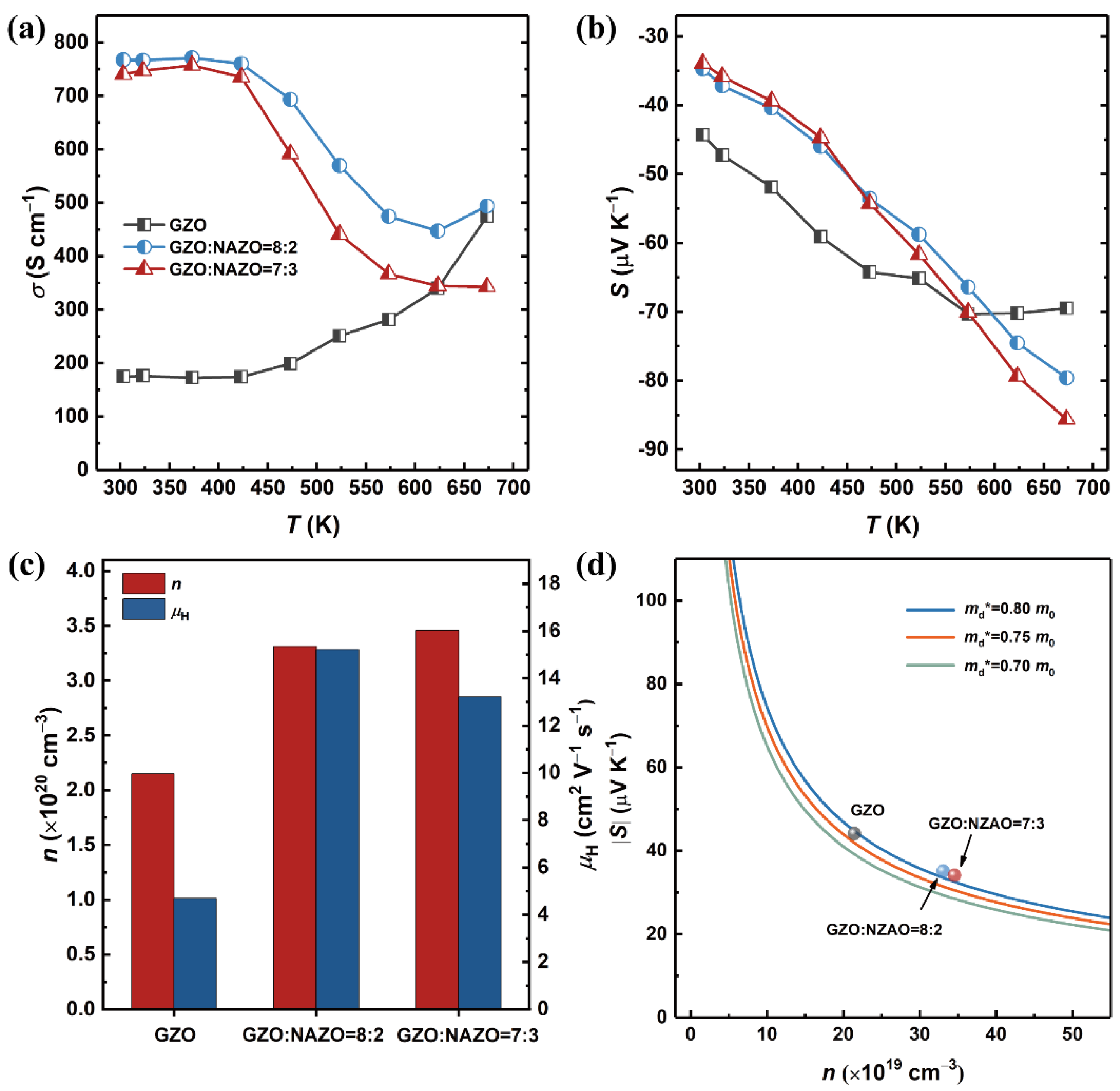
Figure 1. Schematic illustrations showing two kinds of designed thin films, one is GZO film (a), the other is GZO/NAZO film (b); (c) the XRD patterns of GZO and GZO/NAZO thin films; (d) an enlarged section of (002) peaks around 34.5° in (c).
Crystals 12 01351 g001
Figure 2. (a) Cross-section transmission electron microscopy (TEM) image of sample GZO:NAZO = 8:2; (b,c) are enlarged high-resolution TEM (HRTEM) images showing interfaces of Al2O3 substate-GZO and GZO-NAZO, respectively, which are marked as “b” and “c” in (a).
Crystals 12 01351 g002
Figure 3. Electrical properties: (a) temperature-dependent electrical conductivity (σ); (b) temperature-dependent Seebeck coefficient (S); (c) room temperature Hall measurement results, including carrier concentration (n) and Hall mobility (μH); (d) calculated room-temperature Pisarenko plots showing correlations among carrier concentration (n), Seebeck coefficient (S) and DOS effective mass (md*) of samples.
Crystals 12 01351 g003
Figure 4. (a) Temperature-dependent power factor values of GZO thin film and GZO/NAZO thin films; (b) comparison of power factor value of GZO/NAZO thin film in present work and other n-type oxygen-containing thermoelectric materials from references [32,33,34,35].
Crystals 12 01351 g004
Table 1. Electrical transport properties of GZO thin film and GZO/NAZO thin films.
Samplesn (×1020 cm−3)μH
(cm2 V−1 s−1)
md*
(m0)
300 K
σ
(S cm−1)
300/673 K
S
(μV K−1)
300/673 K
PF
(μW m−1 K−2)
300/673 K
GZO2.154.700.78175/475−44/−6932/215
GZO: NAZO = 8:23.3115.220.82767/494−35/−8092/313
GZO: NAZO = 7:33.4613.220.82740/343−34/−8686/252
Publisher’s Note: MDPI stays neutral with regard to jurisdictional claims in published maps and institutional affiliations.

