1. Introduction
Modern displays, solar cells, and other applications need layers as front electrodes that are both conductive and transparent [
1,
2,
3]. The materials of choice are currently oxides of metals such as Ga, In, Cd, Sn, and Zn, so-called transparent conducting oxides (TCOs) [
4]. They all have in common the fact that their conduction band is built from empty
s-orbitals, enabling high electron mobilities.
In 2005, TiO
2−x films doped with Nb were reported also to fulfill the requirements of high transparency and conductivity [
5]. In these materials, electronic transport arises from highly-oriented
d-orbitals [
6], which are less likely to overlap, so that high electron mobilities are not expected. In a previous study, we discussed this issue and the criteria necessary to realize metallic conductivity [
7]. There, it was demonstrated how both metal-like conductivity and high transparency can be achieved in undoped TiO
2−x and why the conductivity values and temperature behavior reported in the literature vary so much.
For all TCOs, including TiO
2−x, charge carriers in addition to the intrinsic ones are necessary to obtain conductivities large enough for applications. This is achieved by doping the matrix oxide with another metal of higher valence. It must have a similar electron configuration as the host to achieve a high doping efficiency. Nb fulfills these criteria for doping of TiO
2, as confirmed by density functional theory (DFT) calculations [
8,
9]. These computations find that Nb leaves the electronic structure of TiO
2 essentially unaltered, so that band transport in Nb-doped TiO
2 is possible. Hence, it is not surprising that many studies focus on this dopant for TiO
2 [
5,
10,
11,
12]. However, in most studies, only one doping level is investigated and highly elaborated production methods are utilized, which are not suitable for large-scale production. Finally, none of them contain a direct comparison with well conductive but undoped films.
Thus, to clarify the influence of Nb doping on the relevant properties, we have investigated different Nb concentrations and compared the results with those for undoped, sub-stoichiometric TiO2−x films. This provides the opportunity to disentangle several effects, including the contribution of oxygen vacancies to the total charge carrier density, or the mobility change with oxygen partial pressure and Nb concentration.
The practical use of a TCO includes the production as thin layers on a large glass surface. Reactive DC magnetron sputtering is capable of doing that and, in addition, provides a larger growth rate than radio-frequency (RF) sputtering of ceramic targets [
13]. Moreover, the understanding of the correlation between Nb content and film properties is vital for optimization and industrial applicability.
The first important property, the crystal structure of a film, has been investigated by X-ray diffraction (XRD). The electrons in the rutile phase of TiO
2 exhibit a very large effective mass inducing hopping transport, as pointed out, among others, by Tang et al. [
14]. Therefore, the phase pureness of anatase is mandatory. Thus, the absence of metallic phases like Nb, Ti, TiO, or other oxides like Nb
2O
5 has to be ensured, and thereby also that Nb is substituting Ti within the crystal.
The main part of this paper investigates the mechanism of charge carrier conduction. We measured the temperature-dependent resistivity (ρ) and Hall effect to derive the density (n) and mobility (µ) of the charge carriers with the intention to determine the doping efficiency of Nb and the mobility limits by comparison with the undoped films. Furthermore, we try to disentangle different phenomena that are not observable when only measuring the resistivity. Finally, ultraviolet and visible light (UV/VIS) spectroscopy has been used to measure the transparency of the films.
2. Materials and Methods
More details of the preparation are reported in [
7]. Borosilicate glass plates (of 20 mm × 20 mm × 0.5 mm) were used as substrates. Optical and electrical measurements were performed on an inner area of 1 cm
2 size surrounded by a groove on which the layer thickness could be measured with a stylus profiler (Dektak XT from Bruker). It has a reproducibility of 0.4 nm, and we used a stylus with a size of 2 µm, force 2 mg, and scan speed usually about 60 µm/s. The accuracy was confirmed by X-ray reflection cross-check measurements (using a PANalytical X’pert Pro system from Philips with CuK
α radiation (λ = 1.5405 Å) and ω/2θ scan from 0° to 150°).
The custom build vacuum chamber was evacuated to a base pressure below 2 × 10⁻⁶ mbar, and a target–substrate distance of 55 mm was chosen. Computer-controlled mass flow controllers inserted argon (purity 4.8, i.e., 99.998 vol%), oxygen (purity 5.5), and nitrogen (purity 5.0), ensuring a constant pressure of 1 Pa during sputtering, monitored by a baratron. Metal targets (pure Ti and doped with 1, 2.5, and 5 at% Nb) with a purity of at least 99.99% were used for reactive DC sputtering at a power of 300 W. Therefore, we assumed that the film had the same composition as the target. For a selection of samples, we checked the Nb concentration by energy-dispersive X-ray spectroscopy EDX, which showed no deviation within the measurement accuracy.
Stoichiometric TiO2 and Nb2O5 do not possess any free electrons and thus are insulators. In order to inject electrons in the conduction band, a slight substoichiometry has to be ensured by precise control of the oxygen partial pressure during sputtering. Therefore, the O2PP has to be continuously measured, which was done by a lambda probe from Zirox.
One hour of pre-sputtering within the oxidic regime [
15] was used to ensure coverage of all surfaces and a steady-state temperature in the whole chamber. No additional heating of the samples was used; thus, the surface temperature was below 60 °C. Starting from the pure metallic/oxygen-free state, we increased the O
2 flux systematically and later decreased it again to record the hysteresis curve O
2PP vs. O
2 flux. A relative O
2PP was employed, defining the 100% point near the last point in the oxidic regime and 0% after the process dropped to the metallic one. This approach is very helpful because the absolute O
2PP values change with target age, sputter power, chamber details, and, what is particularly important in this study, with Nb concentration. More details of how this working point is defined and on the whole sputtering process can be found elsewhere [
7,
16]. It is only by employing such a relative oxygen scale that films with reproducible properties can be achieved, enabling a comparison of different sputter runs and doping concentrations. Even films produced with other sputter parameters, e.g., sputter power or in other vacuum vessels, can be compared.
Highly conductive and transparent films are only obtained when they are deposited within the unstable regime with a partly oxidized target. To keep this process stable, an active process control (APC) is necessary. We used a feedback loop for the sputter power on a 10 ms time scale, working on the difference between the set O2PP and its actually measured value. Sputtering was performed at a time-averaged sputter power of roughly 310 W, the same for all films, after the process had been stabilized on a dummy substrate.
Using this APC, the working point in the unstable regime could be stabilized at an O2PP between 15 and 30 mPa with a constancy of better than ±0.1 mPa. The deposition rate was found to be inversely proportional to the O2PP applied. In the most relevant sputtering regime, i.e., for a power of 300 W and at 70% O2PP, the rates were around 30 nm/min. The deposition times were adapted to create films with thicknesses of about 250 nm. The sample sequence was randomized to avoid potential hidden hysteresis effects from the set parameter O2PP.
The TiO
2−x films were covered with a 34 nm thick Si
3N
4 capping layer to protect the underlying material. Such protection guarantees that the oxide films’ oxygen content remains unchanged under post-heating up to temperatures of 1000 °C [
17]. Si
3N
4 was chosen because it can be deposited as an amorphous film and should not significantly alter the crystallization behavior of TiO
2−x. The layers were reactively sputtered using a pulsed DC generator (210 mA, 1.2 Pa, N
2/Ar ratio of 1/3) without breaking the vacuum.
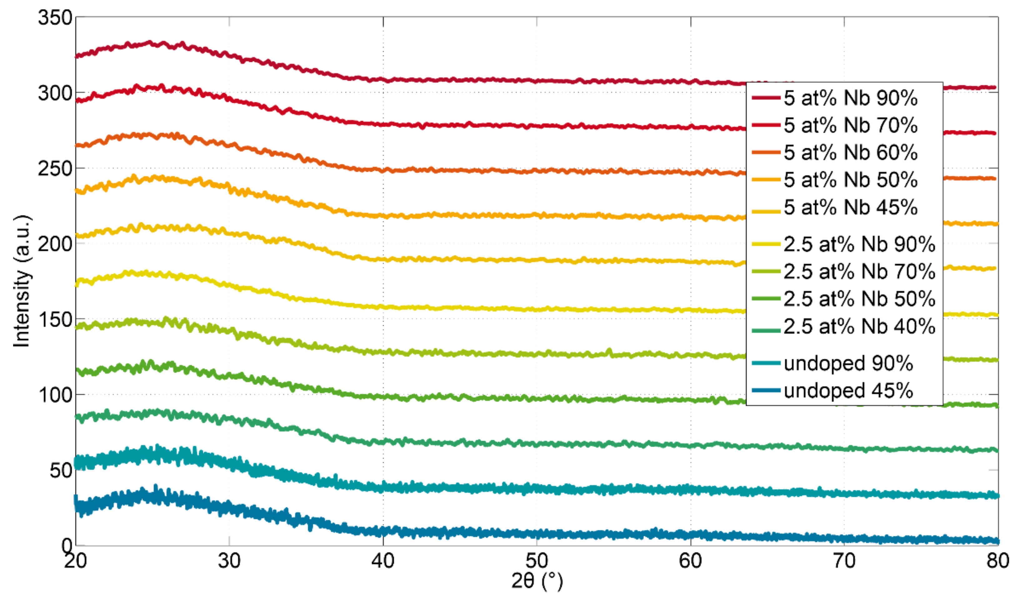
The oxide films were amorphous as-deposited (a selection is shown in
Figure A1) and fully crystallized to anatase (shown in
Figure A2 and [
7]) after annealing at a relatively low temperature of 300 °C for 2 h. This is important, because when the as-deposited films are not entirely amorphous, other studies found that post-heating can result in crystalline mixtures of anatase and rutile, which reduces the conductivity [
18].
As several tests showed no pronounced texture of the films, the structure investigations were performed by XRD at grazing incidence (GI) with a PANalytical X’pert Pro system from Philips with CuKα radiation (λ = 1.5405 Å). The detector angle ϴ was varied between 20° and 80° while keeping the incident angle constant at ω = 0.7° to maximize the interaction volume (stepsize 0.04° and 5 s per step).
Transmission and direct reflection spectra were measured in the wavelength range of 190 nm to 1100 nm with a Lambda 25 UV/VIS system from Perkin Elmer Instruments. In order to get a transparency value that is independent of the interference fringes, we used the envelope method developed by Swanepoel [
19] and convoluted the results with the luminosity function (also called a v-lambda curve, 1931 2° CIE Standard).
The oxide films were provided with electrical contacts in a four-point Van der Pauw geometry using an HB06 wire bonder from TPT. The wedge of this device could penetrate through the Si3N4 capping so that Al wires with a diameter of 33 µm could be soldered to the underlying TiO2−x film on each of the four edges. Each contact showed ohmic current-voltage characteristics. Van der Pauw geometry was chosen because the electrical measurements do not depend on the contact resistances and the exact sample shape. The electrical measurements were performed in two systems from Quantum Design (Physical Property Measurement System and DynaCool), generating magnetic fields up to 9 T and enabling stable temperatures between 1.9 and 400 K. It was found that for the films studied here, sweeping between ±3 T was sufficient (error well below 1%). A linear fit of the measured diagonal resistance as the magnetic field changed then yielded the Hall coefficient and thus the electron density.
Previously, the necessity of a capping layer was illustrated when investigating the TiO
2−x system by showing temperature vs. resistivity data during the annealing of several thin films. Despite Ar flooding, without capping, oxidation was observed, and for higher O
2PP levels during deposition, the films became more resistive, even to the point that they could not be measured at all [
7]. The investigation of the thickness dependence provides another useful test to confirm the stability of the deposition process and the oxidation resistance of the Si
3N
4 layer. Between 100 nm and 1 µm, no systematic resistivity change was observed (e.g., scattering between 200 and 240 µΩcm at 2 K for films doped with 5 at% Nb-doped and an O
2PP of 56%). For even thinner films, the resistivity often starts to increase slightly. To rule out any geometrical influence, we used films of the same thickness of about 250 nm in this investigation.
3. Results and Discussion
A slightly oxygen-poor atmosphere during film growth is necessary to preserve some amount of oxygen vacancies and donor-active dopants in the deposited films. This is true for standard TCOs [
3,
13,
20] as well as for undoped TiO
2 [
7] and is shown here for Nb-doped TiO
2, too. In
Figure 1, the resulting resistivities with respect to the O
2PP are depicted, and in
Table 1 the properties of the most conductive samples for each doping level are summarized. The 1 at% level was omitted as they were not as optimized as the others. The resistivities are remarkably low (630 µΩcm for the 5 at% Nb), considering the simple glass substrate and the low deposition/annealing temperature. For example, Sato et al. reported a value of 1300 µΩcm for DC-sputtered samples with 6.4 at% Nb and annealing at 400 °C in a vacuum [
10], and Oka et al. reported 730 µΩcm with 7 at% Nb and annealing at 600 °C in a vacuum [
21]. Mukherjee et al. used RF sputtering and reported a value of 700 µΩcm with 10 at% Nb after annealing at 400 °C in vacuum [
22]. In these studies, an active process control based on cathode voltage and plasma emission of the Ti was utilized.
The good resistivities in our investigation could be improved even further, e.g., for the 5 at% Nb films to 600 and 550 µΩcm by post-deposition annealing at 400 and 500 °C in Ar atmosphere, respectively. All these films exhibit metal-like conductivity and high transparency, as will be shown later. Films with lower resistivities are possible using a much lower amount of oxygen during sputtering, but they exhibit nearly no transparency anymore.
Although these samples were not produced altogether in one run, not even in the same year, they fit together, when using the relative point in the hysteresis as an ordering scheme. We also tried lower sputtering powers of 100 and 200 W, obtaining similar results.
To understand the origin of this uncommon minimum at O
2PP around 55%, we have to disentangle the contribution of several effects. Generally, conductivity can be described by:
where
e is the elementary charge,
ne,h is the concentration of mobile electrons and holes, and
µe,h is their corresponding mobility. As most TCOs and also TiO
2−x:Nb are n-type semiconductors; their conductivity is governed by electrons. Thus, the contribution of holes to the overall conductivity can be omitted.
The dependency of the free electron concentration (
Figure 2) and their mobility on O
2PP was investigated. As expected, n is reduced by higher amounts of oxygen (fewer oxygen vacancies), whereas it is increased by additional Nb doping. Therefore, the resistivity minimum is achieved with the highest Nb concentration of 5 at% (Nb/Ti ratio) used during this work, indicating that Nb is indeed an effective donor for TiO
2−x.
However, the minimal resistivity with 5 at% Nb is not proportionally lower than with 2.5 at%, as one might expect. Furthermore, the free electron density does not exhibit a corresponding maximum at 55% O2PP but continues to increase for lower values of O2PP. The increase in resistivity with lower O2PP (after the minimum at ~55%) is therefore unexpected.
To explain this discrepancy, we consider the mobility as a function of the free electron density;
µ versus
n, as drawn in
Figure 3. The functional dependence is quite usual for TCOs, as reported for example in [
3,
23,
24]. Here, samples with an O
2PP lower than the resistivity minimum have been neglected, as they show an amorphous microstructure [
7]. On the other hand, some samples annealed at higher temperatures and, especially, a few samples with an Nb concentration of 1 at% have been included. Specimens with different doping concentrations populate different regions in this plot. Although they can possess the same carrier concentration and similar mobility, they rarely have both in common simultaneously. Therefore, one can already conclude that the mobility of free charge carriers in TiO
2−x is not such a direct function of the carrier concentration as, for example, in ZnO:Al [
1,
23] or In
2O
3:Sb [
24]. This means that, in contrast to common TCOs, in TiO
2−x, additional effects have to be present, which significantly influence the mobility, besides the charge carrier concentration.
Figure 4 displays the mobility as a function of the O
2PP. If no Nb is present in the film, the mobility is rising and saturating when increasing the amount of oxygen. This can be understood because a less sub-stoichiometric material contains fewer oxygen vacancies that distort the lattice. A smaller number of such point defects leads to a lattice closer to the ideal TiO
2 crystal lattice, and thus, the mobility increases. Below a specific defect density, the vacancies are not a limiting factor anymore so that the mobility saturates.
In the case of Nb-doping, the relationship between mobility and oxygen content during the sputter process changes dramatically. There, not only does the resulting conductivity exhibit a maximum, but the mobility also does. Obviously, the beneficial effect of high oxygen content and fewer oxygen vacancies is not dominating in Nb-doped films, but is superimposed by an additional effect.
In the presence of Nb, why is the mobility and not only the charge carrier concentration also deteriorating with higher oxygen content? The reason for this could be the strong tendency of Nb to oxidize and to form Nb
2O
5 precipitates/clusters or to bond with oxygen interstitials. DFT calculations support the idea of O
i defects near Nb atoms, which are not present in undoped TiO
2 [
9].
This cluster model is supposed to be present in other TCOs as well, for example, in In
2O
3:Sn at high O
2PP [
2]. However, the tendency of Nb to locally form such clusters and the impact of them seem to be much larger. Using the enthalpies of formation of NbO
2 (−795 kJ/mol) and Nb
2O
5 (−1900 kJ/mol), it can be concluded that the further oxidation of NbO
2 to Nb
2O
5 releases an energy of 155 kJ/mol with respect to Nb (in contrast to a difference of 116 kJ/mol for Sn in Sn
2O
3 (−706 kJ/mol) and SnO
2 (−469 kJ/mol) showing also their lower reactivity [
25]). Thus, if enough thermal energy is provided to enable diffusion of the Nb atoms and also if sufficient oxygen is available, Nb
2O
5 will form. If, on the other hand, an oxygen-poor atmosphere is present, a better comparison is the enthalpy of formation with respect to oxygen. In this case, Nb
2O
5 is indeed slightly less (by ∼18 kJ/mol) favorable than NbO
2, allowing a stable process window for NbO
2.
Moreover, this scenario of further oxidizing NbO
2 can explain why the carrier densities for doped films can reach values as low as for undoped ones (
Figure 4). The harmful effect of the formation of Nb
2O
5 on the sample mobility can be understood in terms of 3D defects. Such insulating (bandgap: E
G > 4.3 eV [
26]) Nb
2O
5 precipitates break the lattice symmetry and distort the surrounding matrix, making them strong scatterers. This is in particular true as in TiO
2 the conduction band is formed by d-orbitals with a highly directional nature in contrast to the s-orbitals of other TCOs.
Fortunately, Nb2O5 is energetically also less favorable, with respect to oxygen, than TiO2 (940 kJ/mol), as otherwise the dopant would reduce the TiO2 and always form this higher-valence oxide.
This cluster model can explain why different doping concentrations populate different regions in
Figure 3, i.e., why, at the same free charge carrier concentration, films with higher Nb content exhibit much lower mobility.
The inserted vertical lines in
Figure 3 denote approximations for the maximum n, which can be achieved at the different doping levels. Varying approaches like additional Si
3N
4 seed layers, lower sputtering powers, or higher annealing temperatures have been tested, especially in the case of the two higher Nb contents. However, all samples seem to reach fundamental limits characteristic of polycrystalline TiO
2−x:Nb films, not only regarding maximum carrier concentration, but, as indicated by the blue line, also regarding maximum mobility. These limits are summarized in
Table 2.
Table 2 also includes the doping efficiency
ν of Nb. Here, the carrier density limit (1 × 10
20 cm
−3) of the undoped samples was subtracted from the electron densities of the doped films. We assumed a constant maximum contribution of oxygen vacancies. Otherwise, the efficiency would reach and even overcome a value of 100% (i.e., one free electron from every Nb atom). Even so, the calculated efficiencies are around 90 % and above, which is quite outstanding for reactively sputtered TCO films, especially without employing high temperatures or hydrogen treatments. For example, in the case of Al in ZnO:Al, maximum efficiencies of typically 50% are reported [
27]. Even films produced very elaborately, exhibiting mobilities and conductivities in the highest possible regime [
28], reach only roughly 75% efficiency, and only by neglecting the contribution of oxygen vacancies as donors.
The linear trend of the relationship between mobility and dopant concentration given by the blue line in
Figure 3 can be used to predict the outcome of a further increase of the Nb content. Such an extrapolation to 10 at% is given in
Table 2, supposing a stable doping efficiency of 90%. Although the maximum mobility is supposed to decrease further, the higher charge carrier density could reduce the resistivity to 390 µΩcm. Reaching such low values for films on glass obtained with a reactive sputter process at room temperature and moderate annealing would be a considerable advancement.
The observation that the maximum achievable mobility decreases with increasing Nb concentration, as indicated by the blue line, can be understood quite intuitively. Even if the maximum is achieved when nearly no Nb2O5 clusters are present, the Nb atoms with their larger ionic radius distort the lattice and thus lower the mobility. Additionally, after they have donated effectively an additional electron into the conduction band, they are more charged, increasing the scattering probability via a larger cross-section.
Such a dominant dependency of the mobility on the dopant concentration indicates that the mobility in TiO
2 is very prone to any kind of lattice distortion. In a previous study about undoped TiO
2 [
7], it was shown that sharply below a specific O
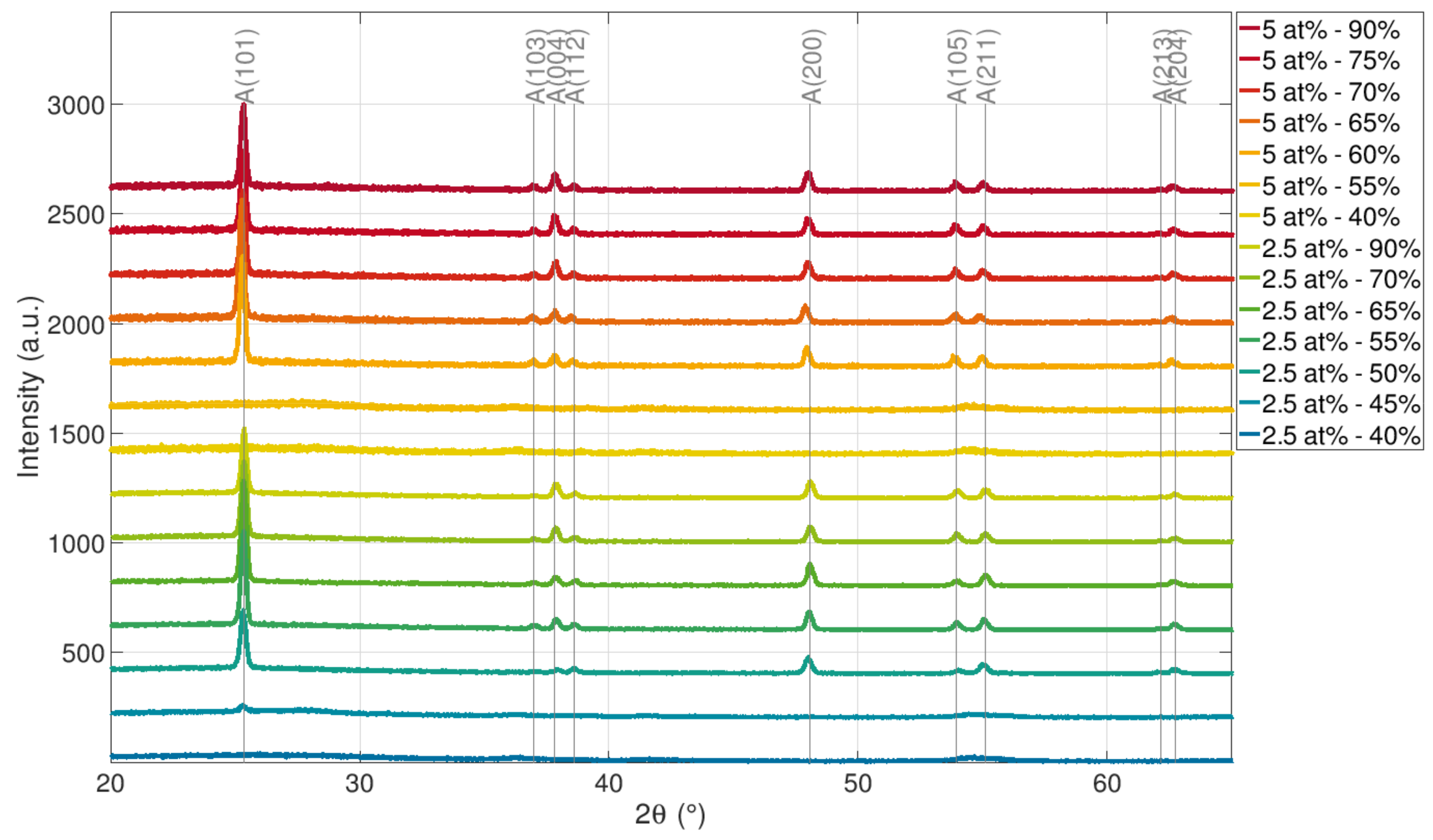
2PP value, the films do not crystallize during annealing even when employing higher temperatures up to 500 °C. The same behavior can also be seen for Nb-doped films, for example, in
Figure 5 (and
Figure A2), where some XRD patterns are displayed. Below an O
2PP of about 50%, the films stay amorphous; this correlates with the nearly zero mobility shown in
Figure 4. Additionally, the films sputtered at higher O
2PP values show slightly reduced intensity despite the same thickness, which also correlates with the decreasing electron mobility.
As stated previously, the difference of several orders of magnitude in electron mobility between the amorphous and crystalline states can be explained by the highly directional nature of d-orbitals that form the conduction band in TiO2. This is in contrast to standard TCOs, where spherical s-orbitals govern the electrical transport, thus not suffering much by an amorphous structure. With this, the high vulnerability of the mobility to the Nb doping and Nb2O5 cluster formation, causing distortions of the lattice, can be understood. However, as can be seen by the absence of any reflexes in the XRD not caused by TiO2 (anatase), there are no precipitations of pure Ti/Nb, Nb2O5, TiO2 (rutile) etc., large enough to be detectable.
To summarize, the minimum of the resistivity as a function of the oxygen partial pressure in
Figure 1 can be explained by a low charge carrier density and mobility caused by Nb
2O
5 cluster formation towards higher O
2PP values and low mobility due to the suppressed crystallization towards lower O
2PP values.
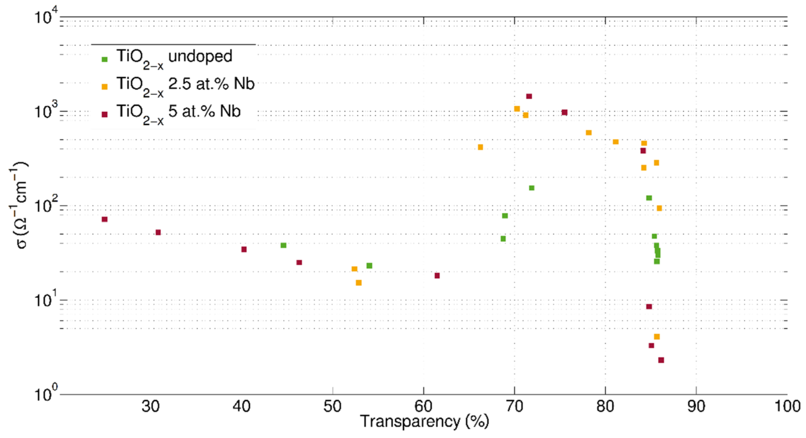
Finally, the transmittance in the visible range has been investigated. The data presented in
Figure 6 demonstrate that a high transmittance above 80% can be achieved. This is the case for wavelengths larger than the fundamental absorption (~350 nm) originating from the bandgap. TiO
2−x films exhibit a high reflectance of about 20% due to their very high refractive index of 2.5, which is characteristic of the anatase phase [
29]. Details about the optical properties of TiO
2−x and the dependency on the O
2PP can be found elsewhere [
7]. As can be seen in
Figure 6, the additional Nb doping had no detrimental effects on the transparency. This indicates that no additional absorption caused by levels introduced in the band gap or metal nanoparticles are present. These findings emphasize an advantage of the TiO
2:Nb system compared to other TCOs: higher dopability without a reduction in transparency. In our films, charge carrier concentrations of up to 1.4 × 10
21 cm
−3 do not show any reduction in transparency compared to films with more than an order of magnitude smaller carrier density.
The higher dielectric constant
ε∞ and effective mass of the electrons
m* in TiO
2 (anatase) reduce the plasma frequency [
30]:
This allows the introduction of a higher carrier density than in standard TCOs before absorption in the red/infrared spectrum becomes important. Therefore, in standard TCOs,
n is less than 1 × 10
21 cm
−3 [
3,
4,
31]. Moreover, the solubility of Nb in TiO
2 is also quite high, and concentrations of up to 10 at% or even 20 at% are possible without formation of precipitates [
5,
32], whereas, e.g., less than 2.5 at% Al in ZnO can be introduced [
33].
On the other spectral side, at the low wavelength regime, we obtained a band gap of 3.3 eV for the undoped TiO2−x and about 3.5 eV ± 0.1 eV for the Nb-doped films, 2.5 at% and 5 at% as well, which are in the range of the measurement uncertainty. The high charge carrier density dominates the behavior for the Nb doped films due to the Burstein–Moss band-filling effect.
Usually, in TCOs, transparency and conductivity are inversely linked, and a tradeoff must be made. This is not so much the case for TiO
2−x:Nb, as optimal transparency and conductivity coincide within the same process window. A common figure of merit proposed by Gordon is the ratio of conductivity σ and absorption coefficient α [
4]:
where
Rsheet is the sheet resistivity, and
T and
R the total transmittance and total reflectance, respectively. He gave some values for TCO materials with different dopants like ZnO:F, In
2O
3:Sn, or SnO
2:Sb, which varied between 0.2 and 7 Ω
−1. Applying this formula, the best films produced in this study, including a Si
3N
4 seed layer and a capping layer, achieved values between 1 and even 6 Ω
−1. As TiO
2 is still a relatively uncommon TCO and was discovered several decades later than the others, we think there is still considerable room for improvement of its performance, e.g., using higher doping concentrations as indicated in
Table 2.


