Article

Effect of Annealing on Innovative CsPbI3-QDs Doped Perovskite Thin Films

1
School of Information Engineering, Jimei University, 183 Yinjiang Road, Jimei, Xiamen 361021, China
2
Department of Applied Physics, National University of Kaohsiung, Kaohsiung University Rd., Kaohsiung 81148, Taiwan
3
School of Opto-Electronic and Communication Engineering, Xiamen University of Technology, Xiamen 361024, China
4
Department of Materials Science and Engineering, Da-Yeh University, Dacun, Changhua 51591, Taiwan
5
Fujian Key Laboratory of Optoelectronic Technology and Devices, Xiamen University of Technology, Xiamen 361024, China
6
Department of Electronic Engineering, I-Shou University, Kaohsiung 84001, Taiwan
7
Department of Electronic Engineering, Cheng Shiu University, Kaohsiung 84008, Taiwan
*
Authors to whom correspondence should be addressed.
Crystals 2021, 11(2), 101; https://doi.org/10.3390/cryst11020101
Submission received: 25 December 2020 / Revised: 20 January 2021 / Accepted: 22 January 2021 / Published: 25 January 2021

Abstract

:
In this study, a simple hot-injection method to synthesize high-quality inorganic perovskite cesium lead iodide (CsPbI3) quantum-dots (QDs) was demonstrated. Adding CsPbI3 QDs into the organic perovskite methylamine lead triiodide (CH3NH3PbI3) to form a composite perovskite film, annealed by different temperatures, was found to be effectively enhanced by the perovskite crystallization. The intensity of the preferred peak (110) of MAPbI3 was enhanced by increasing the size of the crystal and reducing the cluster crystal. The densest film can be found at annealing temperature of 140 °C. The full width half maximum of MAPbI3 and CsPbI3 was analyzed through XRD peak fitting. This was a huge breakthrough for QDs doped perovskite films.

1. Introduction

The past few years, we have witnessed the remarkably rapid development of perovskite solar cells (PSC) [1,2,3]. As the light absorption layer of solar cells, organic perovskite materials MAPbI3 (CH3NH3PbI3) and FAPbI3 (CH5N2PbI3) have attracted much attention due to their suitable energy gap [4,5,6], long carrier diffusion length and impressive light absorption. However, there are still some key shortages for perovskite materials, such as: (1) thermal instability, and (2) they are very sensitive to moisture and oxygen. Therefore, the conversion efficiency of organic perovskite solar cells quickly increased from 9.2% to 20.5% [7,8], but there has been no more obvious promotion until now.
The appearance of perovskite quantum dots (QDs) has further promoted the development of perovskite solar cells. Perovskite quantum dots have become a new type of material because of their excellent optical properties (such as high color purity and narrow emission). Today, the methods for preparing perovskite quantum dots can be divided into two types: (1) ligand-assisted reprecipitation method (LARP) [8], (2) and the hot-injection method (HI) [9]. The disadvantages of the ligand-assisted reprecipitation method are (1) the yield is scarce, (2) the lifetime is very short and (3) the stability of the nanocrystals will be affected because of the addition of N,N-dimethylformamide. Due to its anhydrous, oxygen-free and high-temperature environment, the thermal stability and lifetime of the all-inorganic perovskite quantum dots prepared by the hot-injection method are quite excellent. However, the hot-injection method often requires the Schlenk system to create an anhydrous and oxygen-free environment. Thus, we have improved the hot-injection method by using the glove box system. The precursor, prepared by octadecene (ODE) and oleic acid (OA), is added to the PbI2 solvent. The synthesis temperature was adjusted to produce CsPbI3 quantum dots of different sizes.
Because the crystal structure of MAPbI3 is often fragmented [10], and due to the above shortages, some literature has reported that doping can improve the quality of the film. For example, L.C Chen et al. used doped FAPbI3 QD to enhance the photoelectric conversion efficiency of MAPbI3 [11]; Niu, G et al. used doping Cs ions to improve the thermal stability of MAPbI3 [12]. Since there is no report of the effect by doping all-inorganic quantum dots into MAPbI3 thin films, CsPbI3 is added into MAPbI3 to assist the crystal growth of MAPbI3. Then through the annealing for solution of the thin film, the perovskite composite material is successively deposited on the glass substrate to produce CsPbI3-QDs doped perovskite thin films. This treatment of annealing can effectively remove excess solvent and favor the formation of the perovskite crystal structure. Up to the present, the challenge of thermal stability for the organic-inorganic composite perovskite material still exists [13,14,15], so the control of the annealing temperature is a huge impact on the composition, type and degradation of the perovskite composite film. In this article, a detailed study for the formation mechanism of between structure of crystal and temperature is also presented.

2. Materials and Methods

2.1. Materials

All materials contain Cesium carbonate (Cs2CO3, 99.9%), lead(II) iodide (PbI2, 99.9985%), oleic acid (C₁₈H₃₄O₂, analytical reagent 90%), oleyl amine (C₁₈H₃₅NH₂, 90%), 1-octadecene (ODE, technical grade 90%), toluene (anhydrous, 99.8%), hexane (analytical reagent, 97%), methyl acetate (MeOAc, anhydrous 99.5%), methylammonium iodide (CH3NH3I, 99%), Dimethyl sulfoxide ((CH₃)₂SO, 99%) and gamma-Butyrolactone (C4H6O2, 99.9%) as shown in Table 1. All the chemicals in this work were used without further treatment.

2.2. Solution Preparation and Synthesis for Cs-Oleate Precursor, CsPbI3 QDs and CH3NH3PbI3

The experiment modified the hot-injection method reported by Chenghao Bi et al. [16]. All the experiments were performed in a glove box filled with nitrogen, H2O < 1 ppm and O2 < 1 ppm. The schematic diagram of the experiment is shown in Figure 1.

2.3. Synthesis of Cs-Oleate

Cs2CO3 (0.1 g), OA (0.5 mL) and ODE (10 mL) were loaded into a 50 mL sample bottle and stirred for 1 h at 120 °C. We used heating and air extraction to remove moisture and internal air. Then, the solution was heated at 150 °C until the solution was clear. Finally, the Cs-oleate was stored at 100 °C to avoid precipitation.

2.4. Synthesis of CsPbI3 QDs

Both ODE (10 mL) and PbI2 (0.173 g) were added into a 50 mL sample bottle and were dried at 120 °C for 1 h. Then, OA of 1 mL and OAM of 1 mL (preheated at 70 °C) were poured. The solution was degassed until the PbI2 completely dissolved, and the solution became clear. The solution was then heated to 185 °C. The Cs-oleate (0.0625 M, 1.6 mL) precursor was swiftly injected into the solution. After 5 s, the reaction solution was cooled by immediately immersing the sample bottle into an ice bath.

2.5. Purification of CsPbI3 QD

The prepared CsPbI3 QDs were separated by adding MeOAc (volume ratio of crude solution/MeOAc is 1:3), and then they were centrifuged at 8000 rpm for 5 min. After that, the supernatant was discarded, and the precipitation that contained the QDs was dissolved in 3 mL of hexane. Then, the CsPbI3 QDs were precipitated again by adding MeOAc (volume ratio of crude solution/MeOAc is 1:1) and centrifuging at 8000 rpm for 2 min. Finally, the QDs were dispersed in 3 mL of hexane and centrifuged at 4000 rpm for 5 min to remove excess PbI2 and precursor.

2.6. Synthesis of CH3NH3PbI3

We added CH3NH3I (198.75 mg) and PbI2 (576.25 mg) into the 50 mL sample bottle, and then added C2H6OS (0.5 mL) and C6H6O2 (0.5 mL) into the sample bottle in the glove box and stirred at 300 rpm for 24 h.

2.7. Fabrication of Thin Films

CH3NH3I (50 μL) and CsPbI3 (1 mg) were mixed and spin-coated on the glass substrate in the glove box. Then, CsPbI3-QDs doped perovskite thin films was annealed by different temperatures as shown in Table 2.

2.8. Characteristic Measurements

The absorption spectrums of the thin film were measured by ultraviolet/visible (UV/vis) absorption spectroscopy (HITACHI, U-3900). X-ray diffraction (XRD) data of films were recorded by the Bruker D8 Discover X-ray diffractometer with Grazing Incidence X-Ray Diffraction (GIXRD). Scanning Electron Microscopy (SEM) data of films were recorded by JEOL-6330 Field-Emission SEM, and Photoluminescence (PL) spectrum was recorded by iHR320.

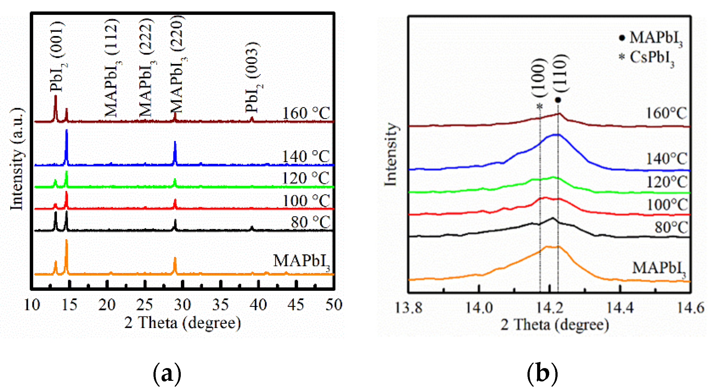
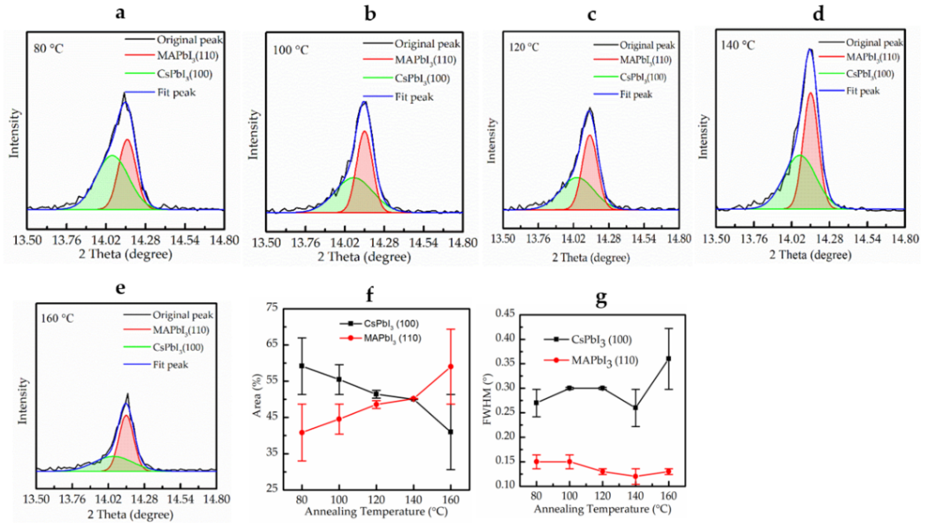
3. Results and Discussion

Figure 2a shows the CsPbI3 quantum dots under UV lamp irradiation. We used different temperatures to synthesize orange wavelength to red wavelength of quantum dots in the glove box and stored QDs in the atmosphere for two weeks. It can be observed that the luminescence properties of the four bottles of quantum dots have not changed a lot, which also represents that we can prepare stable perovskite quantum dots. Figure 2b shows the PL images of CsPbI3 quantum dots at different synthesis temperatures. Due to the quantum confinement effect, as the synthesis temperature increases, the energy level of the quantum dots becomes smaller and causes the emission peak to red shift. We found an unknown emission peak at 663 nm. The intensity of the peak will be enhanced with the increasing of the synthesis temperature. The information of the new peak is not known yet, but it may be due to thermal effects, which are caused by the increasing of the synthesis temperature, and it makes the new emission peak at a long wavelength.
Figure 3 shows the absorption spectrum for QDs doped perovskite thin films. It reveals two peaks of 750 nm and 500 nm that are conjectured due to the α phase and β phase. The annealing temperature was increased from 80 °C to 160 °C, and it is found that the absorption area increased in the entire spectral range (350–850 nm). Then, the absorption area does not increase infinitely with the annealing temperature rising. When the annealing temperature is up to 160 °C, a few yellow spots appear on the surface of the film, as shown in Figure 3b. The morphology of the perovskite yellow phase named β phase will reduce the performance of absorption, resulting in a slight decrease in the absorption area. Compared with pure MAPbI3, the absorption of long-wavelength is improved after the all-inorganic perovskite quantum dots are incorporated. This is due to the fact that the energy gap of CsPbI3 QDs is wider and the small strain occurs at the quantum dot-MAPbI3 interface [17,18]. For short wavelengths, when the annealing temperature is at 80–120 °C, the energy provided by the annealing treatment is not enough to convert precursors such as MAI and PbI2 into perovskite, so the typical absorption peak (500 nm) of perovskite cannot be observed. Thus, most unconverted precursors will affect the absorption capacity of the QDs doped perovskite thin films.
For the CsPbI3-QDs doped perovskite thin films, we discuss its crystal phase. Figure 4a shows the X-ray Diffraction patterns of CsPbI3-QDs doped perovskite thin films. In Figure 4a, it is observed that when the annealing temperature increases, the peak position does not change significantly, and the two strong peaks are observed around 14° and 28°. With the increasing of annealing temperature, the peak position of PbI2 (001) at 13.7° gradually decreases and it vanishes at 140 °C; we know that PbI2 is the precursor of MAPbI3 and CsPbI3. The amount of this compound will affect the efficiency of CsPbI3-QDs doped perovskite thin films as a perovskite solar cell. It can be inferred from the above XRD pattern that 140 °C is indeed the optimal annealing temperature for CsPbI3-QDs doped perovskite thin films. From the literature, it is well known that the peaks of MAPbI3 and CsPbI3 are very close [19,20], so we zoom in the peaks near 14° and 28°, as shown in Figure 4b. It can be found that when the annealing temperature increases, the shape of the peak is no longer symmetrical, and additional peaks appear. It seems this extra peak is the preferred peak of CsPbI3. Therefore, it is necessary that the peak is fitted.
Figure 5 shows the XRD peak fitting patterns of various annealing temperatures and their area, Full width at half maximum (FWHM). From Figure 5a–e, as the annealing temperature increases, the area occupied by MAPbI3 gradually increases, while the peak area occupied by CsPbI3 gradually decreases, until the area reaches 50% when it reaches 140 °C. We concluded that when the peak area ratio of CsPbI3/MAPbI3 is closer to 1, it is most suitable for perovskite crystallization. Meanwhile, the FWHM of MAPbI3 and CsPbI3 is the smallest, which means that the crystallinity of the perovskite is uniform. To perform further evaluation of crystal quality, we also calculated the crystallite size (D) by using Scherrer’s formula [21]:
D = k λ B cos θ
where k is the Scherrer constant, if B is the half-height width of the diffraction peak, then k = 0.89; if B is the integral height and width of the diffraction peak, then k = 1; D is the crystallite size (nm); B is the full width at half maximum of the sample diffraction peak; θ is the Bragg diffraction angle, the unit is angle; γ is the X-ray wavelength (1.54056 Å). From the formula, the average crystallite sizes of pure MAPbI3 and CsPbI3-QDs doped perovskite thin films at different annealing temperatures were estimated to be approximately 72.9, 81.8, 87.1, 78.9, 96.1 and 82.6 nm. The average crystallite size after adding CsPbI3-QDs was larger than pure MAPbI3, and when the annealing temperature was increased to 140 °C, it was the largest average crystallite size. A larger crystallite size will reduce the grain boundaries and further improve the efficiency of the device because the grain boundary is the center of electron-hole recombination.
Figure 6a–f shows the SEM top view of pure MAPbI3 and CsPbI3-QDs doped perovskite thin films at different annealing temperatures. The surface morphology (grain size and shape) of the CsPbI3-QDs doped perovskite thin film changes significantly with the increasing of the annealing temperature. When the annealing temperature is 80 °C to 120 °C, it can be observed that the whole thin films are not dense from Figure 6a–c. These areas uncovered by perovskite will reduce the efficiency of the solar cell because the uncovered part will become an electron trap and make electron-hole recombination around the grain boundary. However, when the annealing temperature increases to 140 °C, the thin film is evenly covered by the perovskite, which will greatly improve the performance of the device, but when the annealing temperature is up to 160 °C, the voids around the perovskite are formed again, resulting in the performance of the device being worse. To further understand the changes in the morphology around the grain boundary, we zoom in the scale to 500 nm, as shown in inset images. When the annealing temperature is 80 °C to 120 °C, both the typical morphology of perovskite and the precursors (MAI, PbI2) can be formed at the same time. Then, a small amount of precursors can be used as an electron blocking layer [22], but excess precursors will lead to dendritic structure and void, causing in the surface of the perovskite film to become rough and to reduce the efficiency of the device. When the annealing temperature is up to 140 °C, the morphology of the perovskite is vastly changed, the original dendrite structure is transformed to a tetragonal structure and the void is also significantly decreased. In inset image of Figure 6f, the large size of the tetragonal structure is formed by a cluster of small perovskite crystallites. The precursor PbI2 surrounds the grain boundary, which makes the surface of the perovskite thin film become rough at 160 °C. Figure 6g–h shows the cross-sectional SEM images. During the experiment, all parameters remained the same except for the composition of the solution doping CsPbI3 QD. The reason for the larger thickness of Figure 6h may be due to the increase of the film formation rate and the increase of the grain size when the Cs ions in the CsPbI3 are introduced into the perovskite thin film [12].
Figure 7 shows the PL spectrum of QD doped perovskite thin films under different annealing temperatures in N2 ambient and pure perovskite. The PL intensity of the perovskite film with doping QD was drastically enhanced compared to that of pure film. It is attributed to the improved crystallinity and larger grain sizes that are consistent with the result of the SEM in Figure 6. When the annealing temperature is up to 140 °C, we observed a slight blue shift and broader peak, which may be caused by the doping CsPbI3-QDs with the wider energy band gap.

4. Conclusions

We improved the hot-injection method and simply prepared all-inorganic perovskite quantum dots with a lifetime of 336 h, and fabricated CsPbI3-QDs doped perovskite thin films by mixing organic perovskite MAPbI3 and all-inorganic perovskite quantum dots CsPbI3. Based on the peaks of the XRD pattern, the FWHM and crystallite size of MAPbI3 and CsPbI3 at different annealing temperatures was analyzed, and the optimal annealing temperature for the composite perovskite thin film was found to be 140 °C. From the SEM image, it was found that the addition of quantum dots and annealing treatment can help perovskite crystallites growth and obtain a dense thin film at 140 °C. Because of the enhancement of crystallinity and larger grain size, the intensity of the PL peak was significantly improved. It can be seen from the above analysis that the QDs doped perovskite thin film plays an important role in the breakthrough of the efficiency of perovskite solar cells.

Author Contributions

Conceptualization, P.-H.H. and Y.-H.C.; Formal analysis, P.-H.H., Y.-H.C. and C.-J.H.; Funding acquisition, P.-H.H. and S.-Y.L.; Investigation, S.-Y.L. and C.-J.H.; Resources, Y.-H.C.; Supervision, N.-F.W., S.-Y.L., K.-W.L. and C.-J.H.; Writing—original draft, Y.-H.C. All authors have read and agreed to the published version of the manuscript.

Funding

This work is sponsored by the Ministry of Science and Technology (MOST) of the Republic of China under contact number of 108-2221-E-390-006.

Conflicts of Interest

The authors declare no conflict of interest.

References

  1. Kojima, A.; Teshima, K.; Shirai, Y.; Miyasaka, T. Organometal halide perovskites as visible-light sensitizers for photovoltaic cells. J. Am. Chem. Soc. 2009, 131, 6050–6051. [Google Scholar] [CrossRef] [PubMed]
  2. Hu, J.H.; Liu, W.H.; Yang, Y.P.; Zhao, L.; Qiao, Y.; Li, S.H.; Chen, M.W. TiO2 nanotube/TiO2 nanoparticle hybrid photoanode for hole-conductor-free perovskite solar cells based on carbon counter electrodes. Opt. Mater. Express 2017, 7, 3322–3331. [Google Scholar] [CrossRef]
  3. Li, X.; Bi, D.; Yi, C.; Décoppet, J.D.; Luo, J.; Zakeeruddin, S.M.; Grätzel, M. A vacuum flash–assisted solution process for high-efficiency large-area perovskite solar cells. Science 2016, 353, 58–62. [Google Scholar] [CrossRef] [PubMed]
  4. Zhao, Z.; Sun, W.; Li, Y.; Ye, S.; Rao, H.; Gu, F.; Huang, C. Simplification of device structures for low-cost, high-efficiency perovskite solar cells. J. Mater. Chem. A 2017, 5, 4756–4773. [Google Scholar] [CrossRef]
  5. Han, T.H.; Tan, S.; Xue, J.; Meng, L.; Lee, J.W.; Yang, Y. Interface and defect engineering for metal halide perovskite optoelectronic devices. Adv. Mater. 2019, 31, 1803515. [Google Scholar] [CrossRef]
  6. Filip, M.R.; Eperon, G.E.; Snaith, H.J.; Giustino, F. Steric engineering of metal-halide perovskites with tunable optical band gaps. Nat. Commun. 2014, 5, 1–9. [Google Scholar] [CrossRef] [Green Version]
  7. Kim, H.S.; Lee, C.R.; Im, J.H.; Lee, K.B.; Moehl, T.; Marchioro, A.; Grätzel, M. Lead iodide perovskite sensitized all-solid-state submicron thin film mesoscopic solar cell with efficiency exceeding 9%. Sci. Rep. 2012, 2, 1–7. [Google Scholar] [CrossRef] [Green Version]
  8. Alharbi, E.A.; Alyamani, A.Y.; Kubicki, D.J.; Uhl, A.R.; Walder, B.J.; Alanazi, A.Q.; Alotaibi, M.H. Atomic-level passivation mechanism of ammonium salts enabling highly efficient perovskite solar cells. Nat. Commun. 2019, 10, 1–9. [Google Scholar] [CrossRef] [Green Version]
  9. Zhang, F.; Zhong, H.; Chen, C.; Wu, X.G.; Hu, X.; Huang, H.; Dong, Y. Brightly luminescent and color-tunable colloidal CH3NH3PbX3 (X = Br, I, Cl) quantum dots: Potential alternatives for display technology. ACS Nano 2015, 9, 4533–4542. [Google Scholar] [CrossRef]
  10. Kumar, A.; Soleimanioun, N.; Singh, N.; Singh, K.L.; Sandhu, I.S.; Tripathi, S.K. Effects of Thermal Annealing Duration on the Film Morphology of Methylamine Lead Triiodide (MAPbI3) Perovskite Thin Films in Ambient Air. J. Nanosci. Nanotechnol. 2020, 20, 3795–3801. [Google Scholar] [CrossRef]
  11. Chen, L.C.; Tien, C.H.; Tseng, Z.L.; Ruan, J.H. Enhanced efficiency of MAPbI3 perovskite solar cells with FAPbX3 perovskite quantum dots. Nanomaterials 2019, 9, 121. [Google Scholar] [CrossRef] [PubMed] [Green Version]
  12. Niu, G.; Li, W.; Li, J.; Liang, X.; Wang, L. Enhancement of thermal stability for perovskite solar cells through cesium doping. RSC Adv. 2017, 7, 17473–17479. [Google Scholar] [CrossRef] [Green Version]
  13. Kumar, G.R.; Savariraj, A.D.; Karthick, S.N.; Selvam, S.; Balamuralitharan, B.; Kim, H.J.; Prabakar, K. Phase transition kinetics and surface binding states of methylammonium lead iodide perovskite. Phys. Chem. Chem. Phys. 2016, 18, 7284–7292. [Google Scholar] [CrossRef]
  14. Stoumpos, C.C.; Malliakas, C.D.; Kanatzidis, M.G. Semiconducting tin and lead iodide perovskites with organic cations: Phase transitions, high mobilities, and near-infrared photoluminescent properties. Inorg. Chem. 2013, 52, 9019–9038. [Google Scholar] [CrossRef] [PubMed]
  15. Li, Z.; Yang, M.; Park, J.S.; Wei, S.H.; Berry, J.J.; Zhu, K. Stabilizing perovskite structures by tuning tolerance factor: Formation of formamidinium and cesium lead iodide solid-state alloys. Chem. Mater. 2016, 28, 284–292. [Google Scholar] [CrossRef]
  16. Fang, F.; Chen, W.; Li, Y.; Liu, H.; Mei, M.; Zhang, R.; Wang, K. Employing polar solvent controlled ionization in precursors for synthesis of high-quality inorganic perovskite nanocrystals at room temperature. Adv. Funct. Mater. 2018, 28, 1706000. [Google Scholar] [CrossRef]
  17. Smith, A.M.; Mohs, A.M.; Nie, S. Tuning the optical and electronic properties of colloidal nanocrystals by lattice strain. Nat. Nanotechnol. 2009, 4, 56–63. [Google Scholar] [CrossRef] [Green Version]
  18. Luo, S.; Kazes, M.; Lin, H.; Oron, D. Strain-induced type II band alignment control in CdSe nanoplatelet/ZnS-sensitized solar cells. J. Phys. Chem. C 2017, 121, 11136–11143. [Google Scholar] [CrossRef]
  19. Zhang, T.; Dar, M.I.; Li, G.; Xu, F.; Guo, N.; Grätzel, M.; Zhao, Y. Bication lead iodide 2D perovskite component to stabilize inorganic α-CsPbI3 perovskite phase for high-efficiency solar cells. Sci. Adv. 2017, 3, e1700841. [Google Scholar] [CrossRef] [Green Version]
  20. Pratiwi, Z.R.; Nuraeni, L.; Aimon, A.H.; Iskandar, F. Morphology control of MAPbI3 perovskite thin film as an active layer of solar cells. IOP Conf. Ser. Mater. Sci. Eng. 2018, 395, 012010. [Google Scholar] [CrossRef] [Green Version]
  21. Khadka, D.B.; Shirai, Y.; Yanagida, M.; Masuda, T.; Miyano, K. Enhancement in efficiency and optoelectronic quality of perovskite thin films annealed in MACl vapor. Sustain. Energy Fuels 2017, 1, 755–766. [Google Scholar] [CrossRef]
  22. Zhao, Y.; Li, Q.; Zhou, W.; Hou, Y.; Zhao, Y.; Fu, R.; Zhao, Q. Double-Side-Passivated Perovskite Solar Cells with Ultra-low Potential Loss. Solar RRL 2019, 3, 1800296. [Google Scholar] [CrossRef]
Figure 1. (ac). Schematic diagram of perovskite quantum dots and fabrication of thin film.
Crystals 11 00101 g001
Figure 2. (a) Colloidal solutions at different synthesis temperatures in toluene under UV lamp (λ = 365 nm). (b) CsPbI3-QD (0 h) at different synthesis temperatures.
Crystals 11 00101 g002aCrystals 11 00101 g002b
Figure 3. (a) Absorption spectrum for CsPbI3-QDs doped perovskite thin films under different annealing temperatures and pure perovskite (MAPbI3). (b) The morphology of the CsPbI3-QDs doped perovskite thin films by camera (α phase and β phase).
Crystals 11 00101 g003
Figure 4. (a) XRD patterns of CsPbI3-QDs doped perovskite thin films obtained by different annealing temperatures. (b) XRD patterns under the scale of 13.8°~14.6°.
Crystals 11 00101 g004
Figure 5. (ae) XRD fitting patterns. (f,g) Area and FWHM of CsPbI3-QDs doped perovskite thin films at different annealing temperatures.
Crystals 11 00101 g005
Figure 6. SEM images (top view) of (a) pure MAPbI3 and (bf) CsPbI3-QDs doped perovskite thin films at different annealing temperatures with scale size of 2 μm and inset images are 500 nm. (g,h) Cross-sectional SEM images of pure MAPbI3 and CsPbI3-QDs doped perovskite thin films at 140 °C.
Crystals 11 00101 g006
Figure 7. PL spectrum for CsPbI3-QDs doped perovskite thin films under different annealing temperatures in N2 ambient and pure perovskite (MAPbI3).
Crystals 11 00101 g007
Table 1. Preparation parameters of Cs-Oleate Precursor, CsPbI3 QDs and CH3NH3PbI3.
Cs-Oleate PrecursorSynthesis of CsPbI3 QDSynthesis of MAPbI3
Cs2CO3 0.1 gPbI2 0.173 gCH3NH3I 198.75 g
Oleic acid 0.5 mL1-octadecene 10 mLPbI2 576.25 g
1-octadecene 10 mLOleic acid 1 mLC2H6OS 0.5 mL
Oleyamine 1 mLC6H6O2 0.5 mL
Cs-oleate precursor 1.6 mL
Table 2. Parameter of annealing temperatures.
Annealing TemperatureTime
80–160 °C15 min
Publisher’s Note: MDPI stays neutral with regard to jurisdictional claims in published maps and institutional affiliations.

