Article

High-Speed and High-Power 940 nm Flip-Chip VCSEL Array for LiDAR Application

1
Department of Photonics, College of Electrical and Computer Engineering, National Yang Ming Chiao Tung University, Hsinchu 30010, Taiwan
2
Semiconductor Research Center, Hon Hai Research Institute, Taipei 11492, Taiwan
3
iReach Corporation, Hsinchu 30844, Taiwan
*
Author to whom correspondence should be addressed.
Crystals 2021, 11(10), 1237; https://doi.org/10.3390/cryst11101237
Submission received: 24 September 2021 / Revised: 10 October 2021 / Accepted: 12 October 2021 / Published: 14 October 2021

Abstract

:
In this paper, we demonstrate the design and fabrication of a high-power, high-speed flip-chip vertical cavity surface emitting laser (VCSEL) for light detection and ranging (LiDAR) systems. The optoelectronic characteristics and modulation speeds of vertical and flip-chip VCSELs were investigated numerically and experimentally. The thermal transport properties of the two samples were also numerically investigated. The measured maximum output power, slope efficiency (SE) and power conversion efficiency (PCE) of a fabricated flip-chip VCSEL array operated at room-temperature were 6.2 W, 1.11 W/A and 46.1%, respectively. The measured L-I-V curves demonstrated that the flip-chip architecture offers better thermal characteristics than the conventional vertical structure, especially for high-temperature operation. The rise time of the flip-chip VCSEL array was 218.5 ps, and the architecture of the flip-chip VCSEL with tunnel junction was chosen to accommodate the application of long-range LiDAR. The calculated PCE of such a flip-chip VCSEL was further improved from 51% to 57.8%. The device design concept and forecasting laser characteristics are suitable for LiDAR systems.

1. Introduction

The vertical cavity surface emitting laser (VCSEL) is considered to be a significant light source for sensing/imaging systems owing to its excellent beam quality [1], low threshold [2], low-energy consumption, low-cost [3], compact size and high reliability. Nowadays, commercial three-dimensional depth sensing applications are ubiquitous, such as for gestures [4], face recognition, autofocus [5] and eye movement tracking [6]. The spectral width of a surface-emitting laser beam is relatively narrow, and the temperature dependence of the wavelength is roughly 0.07 nm/K, which enables VCSELs to be competitive in 3D sensing [7,8]. This functionality allows VCSELs to be utilized with narrowband filters to filter out unwanted ambient signals [9], improve the signal-to-noise ratio (SNR), and increase the accuracy of outdoor sensing.
The majority of VCSEL arrays are almost entirely made up of vertical structures [10,11,12]. It is worth mentioning that when the VCSEL is operating at a higher injection current, the thick epitaxial substrate produces an enormous amount of heat and a drop in the PCE; additionally, earlier roll-over behaviors and a lower response speed have been observed [13].
Moreover, the conventional vertical device requires an increase in the height of the device to deal with the wire bonding process and this also increases the cost of the package. A flip-chip like structure can reduce the cost of the sensor module because there is no need for wire bonding and the device is thinner and has less area. By removing wire bonding, the parasitic inductance and resistance of the device can be further reduced, thus improving the rise time [14]. This can provide superior depth resolution under high-frequency operation.
For thermal management challenges, a flip-chip like VCSEL has a high probability of providing greater heat dissipation [15,16], which is beneficial for improving the device’s optoelectronic characteristics and response speed.
In this paper, we propose a flip-chip VCSEL with substrate removal and coplanar electrodes, which emits the light directly upward through the transparent sapphire substrate. First, we developed 3D simulation models to examine the thermal and optoelectronic properties of vertical and flip-chip VCSELs, such as the L-I-V curve and response speed. Then, the two kinds of VCSELs and their respective VCSEL arrays were fabricated. Finally, the laser characteristics were measured to verify the design concepts.
Furthermore, a single VCSEL’s output power is relatively low for middle and long-distance LiDAR applications due to the small active volume compared to a laser diode and distributed feedback laser [17]. For middle and long-distance applications, the light power of a single VCSEL and VCSEL array must be increased. With regard to the design of a high-power VCSEL, we adopted the highly doped GaAs tunnel junction (TJ) to cascade the two pairs of active regions to numerically demonstrate the advantage of the GaAs TJ in power improvement.

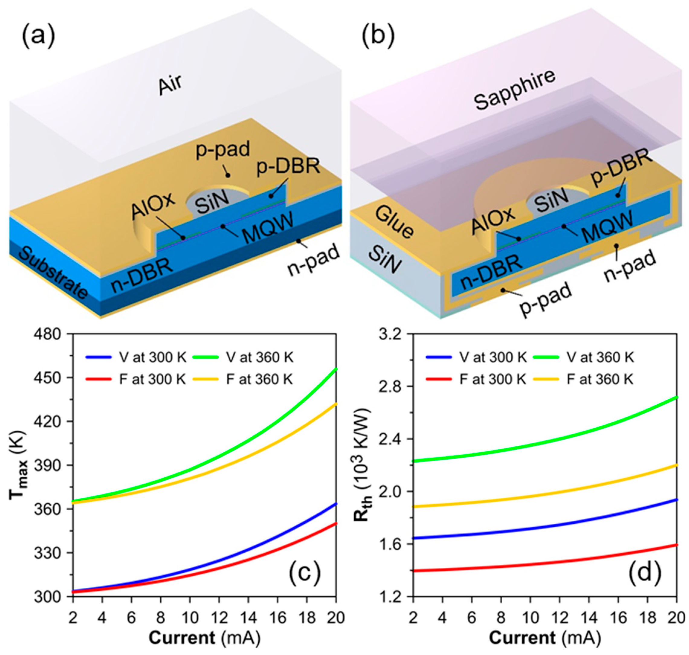
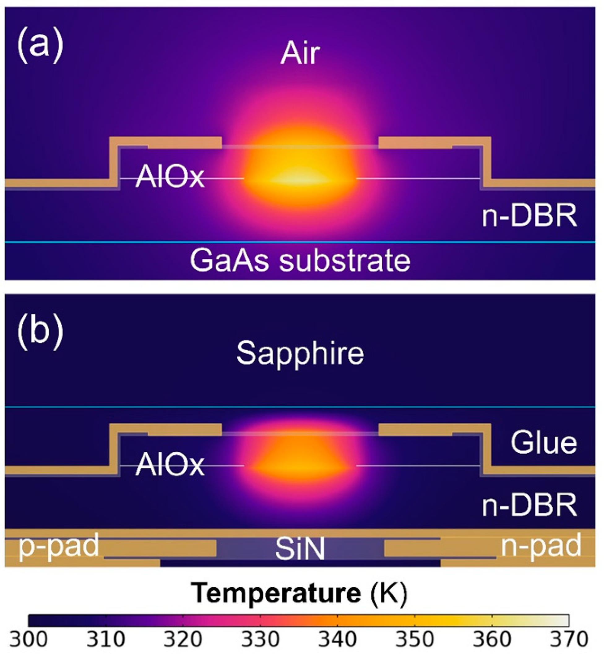
2. Device Structure Design and Fabrication

The epitaxial p-i-n structure of a 940 nm VCSEL was composed of a 100 μm-thick GaAs substrate, a distributed Bragg reflector (DBR) composed of 34 pairs of n-doped Al0.05Ga0.95As/Al0.95Ga0.05As, 3 pairs of multiple quantum wells (MQWs) with a 10 nm GaAs barrier and 8 nm InGaAs quantum well, followed by a DBR composed of 16 pairs of p-doped Al0.95Ga0.05As/Al0.05Ga0.95As. Then, a 10 μm AlOx current aperture was placed at the antinode of the simulated vertical standing wave pattern. The fabrication process was as follows: a p-type ring-shaped metal contact is deposited through electron beam (E-beam) evaporation, and a p-side mesa was created by inductively coupled plasma-reactive ion etching (ICP-RIE). Then, the oxide aperture was formed by the wet oxidation process. After that, a 200 nm SiNx passivation was deposited by plasma-enhanced chemical vapor deposition (PECVD) followed by the deposited of p-pad by E-beam. These steps were used for the vertical VCSEL and the preliminary process of the flip-chip VCSEL. Subsequently, the VCSEL wafer was bonded onto sapphire by adhesive glue, and the original GaAs substrate was removed by wet etching. Then, we used ICP-RIE and E-beam processes to etch an n-side mesa and deposit n-type metal, respectively. After that, PECVD was used to deposit the SiNx insulating layer, metal connections and SiNx passivation, which were deposited in sequence. Finally, the coplanar electrodes p-pad and n-pad were formed to complete the vertical (V) and flip-chip (F) VCSEL structures as shown in Figure 1a,b.

3. Comparison of Vertical and Flip-Chip VCSEL

3.1. Numerical Analysis

We used the commercial device simulation software, photonic integrated circuit simulator in 3D (PICS3D) to calculate the L-I-V curves and rise times of single vertical and flip-chip VCSELs. We also used COMSOL to explore the difference in thermal dissipation between vertical and flip-chip VCSEL structures. The heat sources used in the 3D VCSEL thermal model were taken from simulated L-I-V curves.
The calculated junction temperature (Tmax) and thermal resistance (Rth) are shown in Figure 1c,d. Obviously, the current-dependent Tmax and Rth of sample F at 300 K and 360 K are always lower than that of sample V, implying that the thermal dissipation ability of our proposed flip-chip VCSEL is beneficial for high-current operation, particularly for higher ambient temperatures. The fundamental reason is that the flip-chip VCSEL eliminates the thicker GaAs substrate, allowing heat generated in the active region to be dissipated more effectively through the bottom heat sink. Additionally, the simulated temperature distributions of samples V and F at a current injection of 20 mA and an ambient temperature of 300 K are shown in Figure 2. The thermal conductivities of GaAs-based semiconductors and sapphire used in the simulation model were referenced from previous research [18,19]. Moreover, the thermal conductivities of air and adhesive glue were considered as 0.0255 W/(m·K) and 0.25 W/(m·K), respectively. Correspondingly, the simulated temperatures at the glue on the top surface of the VCSEL and n-DBR region of sample F are clearly lower than those of sample V. The thermal accumulation for a flip-chip VCSEL can be quickly mitigated, which can be attributed to the substrate removal and the relatively higher thermal conductivity of sapphire compared to air.

3.2. L-I-V Characteristics

On the other hand, the simulated L-I-V curves of vertical and flip-chip 940 nm VCSELs at 300 K and 360 K are shown in Figure 3a,b. We can observe that the flip-chip VCSEL with the GaAs substrate removal process has a higher slope efficiency (SE) and a larger roll-over current at 300 K and 360 K. This improvement can be attributed to the enhanced thermal dissipation of the flip-chip VCSEL. In addition, the carriers will escape from MQW when the injected current increases due to the increase in kinetic energy of carriers as the temperature rises [20,21,22]. As a result of this effect, slope efficiency and output power will be reduced. However, it can be seen that both vertical and flip-chip VCSELs require a higher current to reach the threshold when the ambient temperature reaches 360 K. This is because the increase in temperature will reduce the gain of the material. The QWs must receive a higher current to provide sufficient gain to overcome the loss and reach the threshold condition [23]. The better thermal dissipation of the flip-chip VCSEL can reduce the rise of the threshold current.
Figure 3c,d show the measured L-I-V curves of fabricated vertical and flip-chip VCSELs with continuous wave (CW) operation. The slope efficiency and power conversion efficiency (PCE) of the vertical VCSEL array are 0.93 W/A and 44%, and in the case of the flip-chip VCSEL array, these two efficiencies are 1.12 W/A, and 49%, respectively. The measurements obviously indicate that although the power characteristics are slightly smaller than the numerical simulation, the trend in the comparison between the vertical and the flip-chip VCSELs is consistent with the simulation results. The flip-chip VCSEL exhibits better heat dissipation and also achieves better SE, PCE, and roll-over current by removing the thick GaAs substrate.
In order to realize higher output power for LiDAR applications, vertical and flip-chip VCSEL arrays were fabricated. Figure 4a,b express the measured L-I-V curves of fabricated vertical and flip-chip VCSEL arrays under CW operation. The number of VCSEL arrays is 621 with a length of 1075 µm and a width of 1060 µm. The maximum output powers (SE, PCE) of the vertical and flip-chip VCSEL arrays operated at 300 K are 4.73 W (0.91 W/A, 41.3%), and 6.2 W (1.11 W/A, 46.1%), respectively. Additionally, under the operating current of 5.5 A, there are 61% and 27% reductions in output power between 300 K and 360 K for vertical and flip-chip VCSEL arrays, respectively. This proves that the flip-chip VCSEL array possesses significantly better electrical and optical properties than the vertical VCSEL array. Moreover, the small discrepancy between the simulated and measured results is due to the thermal crosstalk effect [24]. Flip-chip VCSEL arrays can be operated at a larger current regardless of whether at room temperature or high temperature.

3.3. Modulation Response

The resolution of LiDAR imaging depends on the light modulation speed and contrast of the device [25]. The excellent thermal dissipation of the flip-chip VCSEL makes it more competitive in high-power applications because it reduces unnecessary losses caused by heat, and even enhances the modulation response speed.
To calculate the modulation response of VCSEL, the built-in temperature-dependent optoelectronic parameters including carrier recombination (radiative and Auger), valence band absorption, QW gain coefficient and refractive index were considered. The simulated modulation responses of samples V and F are shown in Figure 4c. It can be seen that there is a significant difference in modulation response between the two samples. The calculated rise times for samples V and F are 175 ps and 142 ps, respectively. The intrinsic modulation response of the VCSEL is related to internal quantum efficiency and differential gain [26]. The heat generation will cause carrier overflow, thus lowering the internal quantum efficiency and differential gain in D factor [27], and resulting in decreasing modulation speed. Therefore, the thermal dissipation characteristics of the flip-chip VCSEL not only increase the SE, PCE and roll-over current, but also improve the modulation response.
To measure the dynamic characteristics, we used the bias tee and the network analyzer to modulate vertical and flip-chip VCSEL arrays as well as measure the rise times when the bias current was set to 1.3 times the threshold current. The full width at half maximum (FWHM) bandwidths of the signals for two VCSEL arrays were all 1.997 ns, and the signal amplitudes of the vertical and flip-chip VCSEL arrays were 1.725 mV and 1.65 mV, respectively. The normalized modulation responses are plotted in Figure 5d and the measured rise times of the vertical and flip-chip VCSEL arrays were 237.2 ps and 218.5 ps, respectively, under 500 MHz modulation. It is again clearly demonstrated that the flip-chip VCSEL array can obtain a faster rise time due to better thermal dissipation and less parasitic impedance, making it suitable for the development of high-speed and high-power LiDAR.

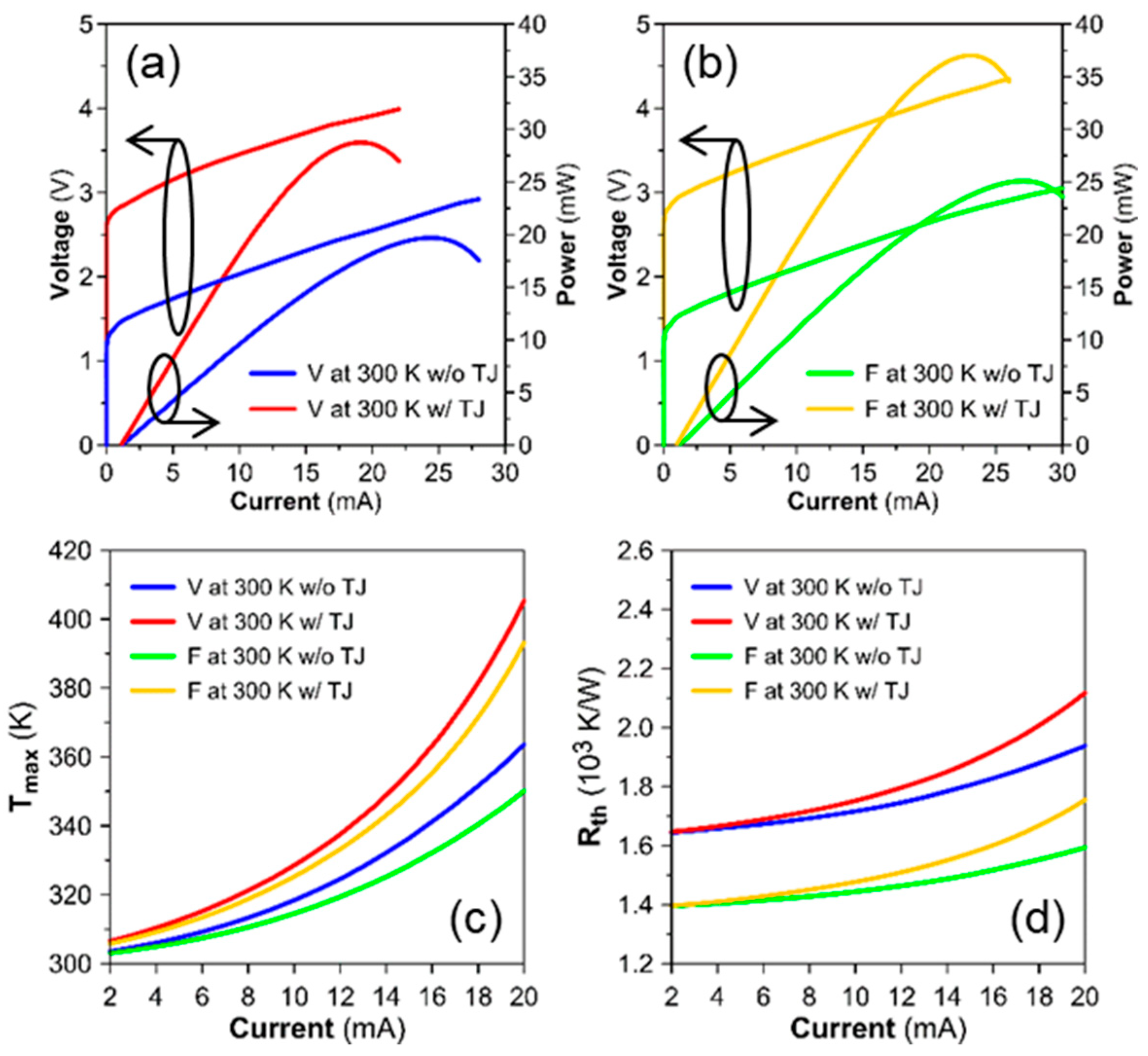
4. Simulation of VCSEL with Tunnel Junction

In order to increase the output power, we applied a high doped GaAs TJ to cascade the two active regions and we analyzed the L-I-V and thermal characteristics of vertical and flip-chip VCSELs.
Figure 5a,b display the simulated L-I-V curves of samples V and F with a GaAs TJ at 300 K. Consequently, the maximum output powers (PCE) of these two samples with GaAs TJ increased from 19.2 mW (46%) and 23.3 mW (51%) to 28.6 mW (53.2%) and 37.1 mW (57.8%), respectively. The use of the tunnel junction will increase the output power; however, this will also slightly increase the junction temperature and accelerate the roll-over current for operating at higher current injection.
Similar to Figure 1c,d, the simulated current-dependent Tmax and Rth for two samples with a highly doped GaAs TJ are shown in Figure 5c,d, and as a result, the calculated Tmax (Rth) for vertical and flip-chip VCSELs operated at 20 mA were 405.8 K (2110 K/W) and 392.1 K (1930 K/W), respectively. Compared to the vertical type, the flip-chip VCSEL with TJ can still maintain better thermal characteristics and it appears that sample F with GaAs TJ is preferable for long-range LiDAR application.

5. Conclusions

In this paper, we have numerically and experimentally investigated the thermal and optoelectronic characteristics of vertical and flip-chip VCSELs and the pertinent VCSEL arrays. A 3D VCSEL thermal model based on commercial FEM software was used to analyze the temperature distribution caused by a three-dimensional heat source. Calculated results indicated that the flip-chip VCSEL has superior heat dissipation. The additional improvement in the output power, SE and PCE were achieved by using the GaAs substrate removal technique. Due to the excellent thermal dissipation of our proposed flip-chip VCSEL, as expected, the measured output power, SE and PCE of the flip-chip VCSEL array under CW operation can reach 6.2 W, 1.11 W/A and 46.1%, respectively. In addition, the measured rise time of the flip-chip VCSEL can be reduced from 237.2 ps to 218.5 ps at a small current. In order to further enhance the device characteristics, a simulation model for a single VCSEL incorporated with highly doped GaAs TJ was constructed. The numerical results revealed that the calculated output power and PCE for the proposed flip-chip VCSEL with a GaAs TJ structure increased from 23.3 mW to 37.1 mW and 51% to 57.8%, respectively. The overall results suggest that the high-power and highspeed laser device composed of the array of the proposed flip-chip VCSEL with GaAs TJ can be fully applied for long-range LiDAR applications.

Author Contributions

Conceptualization, K.-B.H. and G.-H.C.; methodology, D.Y. and Z.-K.L.; software, D.Y. and K.-B.H.; validation, H.-C.K.; formal analysis, Z.-K.L., D.Y. and G.-H.C.; investigation, H.-C.C., D.Y. and G.-H.C.; resources, S.-L.C. and H.-C.K.; data curation, K.-B.H., G.-H.C. and Z.-K.L.; writing—original draft preparation, W.-T.H., D.Y. and G.-H.C.; writing—review and editing, K.-B.H. and W.-T.H.; visualization, H.-C.K.; supervision, H.-C.K.; project administration, S.-L.C. and H.-C.K.; funding acquisition, H.-C.K. All authors have read and agreed to the published version of the manuscript.

Funding

This research was funded by the Ministry of Science and Technology, Taiwan (110-2124-M-A49-003-, 108-2221-E-009-113-MY3).

Data Availability Statement

Data sharing not applicable.

Acknowledgments

The authors would like to thank iReach Corporation and Epistar Corporation for the helpful discussion.

Conflicts of Interest

The authors declare no conflict of interest.

References

  1. Pan, G.; Xu, C.; Xie, Y.; Dong, Y.; Wang, Q.; Deng, J.; Xun, M.; Chen, H. Enhancing beam quality and optical intensity of partially coherent VCSEL array by on-chip integrating micro optical phase modulators. Jpn. J. Appl. Phys. 2019, 58, 080905. [Google Scholar] [CrossRef]
  2. Pan, G.; Xie, Y.; Xu, C.; Xun, M.; Dong, Y.; Deng, J.; Chen, H.; Sun, J. Dependence of Beam Quality on Optical Intensity Asymmetry in In-Phase Coherently Coupled VCSEL Array. IEEE J. Quantum Electron. 2018, 54, 1–6. [Google Scholar] [CrossRef]
  3. Koyama, F. Recent Advances of VCSEL Photonics. J. Light. Technol. 2006, 24, 4502–4513. [Google Scholar] [CrossRef]
  4. Moser, P.; Lott, J.A.; Larisch, G.; Bimberg, D. Impact of the Oxide-Aperture Diameter on the Energy Efficiency, Bandwidth, and Temperature Stability of 980-nm VCSELs. J. Light. Technol. 2015, 33, 825–831. [Google Scholar] [CrossRef]
  5. Robertson, J.; Hejda, M.; Bueno, J.; Hurtado, A. Ultrafast optical integration and pattern classification for neuromorphic photonics based on spiking VCSEL neurons. Sci. Rep. 2020, 10, 1–8. [Google Scholar] [CrossRef] [Green Version]
  6. Khaldi, A.; Daniel, E.; Massin, L.; Kärnfelt, C.; Ferranti, F.; Lahuec, C.; Seguin, F.; Nourrit, V.; Tocnaye, J.-L.D.B.D.L. A laser emitting contact lens for eye tracking. Sci. Rep. 2020, 10, 1–8. [Google Scholar] [CrossRef]
  7. Lindemann, M.; Jung, N.; Stadler, P.; Pusch, T.; Michalzik, R.; Hofmann, M.R.; Gerhardt, N.C. Bias current and temperature dependence of polarization dynamics in spin-lasers with electrically tunable birefringence. AIP Adv. 2020, 10, 035211. [Google Scholar] [CrossRef]
  8. Michalzik, R. VCSEL Fundamentals. In VCSELs: Fundamentals, Technology and Applications of Vertical-Cavity Surface-Emitting Lasers; Michalzik, R., Ed.; Springer: Berlin/Heidelberg, Germany, 2013; pp. 19–75. [Google Scholar]
  9. Hu, J.; Liu, B.; Ma, R.; Liu, M.; Zhu, Z. A 32x 32-Pixel Flash LiDAR Sensor With Noise Filtering for High-Background Noise Applications. IEEE Trans. Circuits Syst. I. Regul. Pap. 2021, PP, 1–12. [Google Scholar] [CrossRef]
  10. Khan, Z.; Shih, J.-C.; Chao, R.-L.; Tsai, T.-L.; Wang, H.-C.; Fan, G.-W.; Lin, Y.-C.; Shi, J.-W. High-brightness and high-speed vertical-cavity surface-emitting laser arrays. Optica 2020, 7, 267. [Google Scholar] [CrossRef]
  11. Safaisini, R.; Joseph, J.R.; Lear, K.L. Scalable High-CW-Power High-Speed 980-nm VCSEL Arrays. IEEE J. Quantum Electron. 2010, 46, 1590–1596. [Google Scholar] [CrossRef]
  12. Zhang, J.; Ning, Y.; Zhang, X.; Hofmann, W.; Liu, K.; Zhang, J.; Qiu, J.; Zeng, Y.; Fu, X.; Huang, Y.; et al. 910 nm vertical-cavity surface-emitting laser arrays with 100 W output power level and low driving current. Jpn. J. Appl. Phys. 2018, 57, 100302. [Google Scholar] [CrossRef]
  13. Bowers, J. High speed semiconductor laser design and performance. Solid-State Electron. 1987, 30, 1–11. [Google Scholar] [CrossRef]
  14. Arslan, S.; Shah, S.A.A.; Kim, H. Power Efficient Current Driver Based on Negative Boosting for High-Speed Lasers. Electronics 2019, 8, 1309. [Google Scholar] [CrossRef] [Green Version]
  15. Mehandru, R.; Dang, G.; Kim, S.; Ren, F.; Hobson, W.; Lopata, J.; Pearton, S.; Chang, W.; Shen, H. Finite difference analysis of thermal characteristics of CW operation 850 nm lateral current injection and implant-apertured VCSEL with flip-chip bond design. Solid-State Electron. 2002, 46, 699–704. [Google Scholar] [CrossRef]
  16. Al-Omari, A.N.; Lear, K.L. Fabrication and performance of bottom-emitting flip-chip bonded 980 nm vertical-cavity lasers with copper- and indium-plated heat-sinks. Semicond. Sci. Technol. 2011, 26, 125020. [Google Scholar] [CrossRef]
  17. Matsuo, S.; Kakitsuka, T. Low-operating-energy directly modulated lasers for short-distance optical interconnects. Adv. Opt. Photonics 2018, 10, 567–643. [Google Scholar] [CrossRef]
  18. Tiwari, S. Compound Semiconductor Device Physics; Elsevier BV: Amsterdam, The Netherlands, 1992. [Google Scholar]
  19. Roshan, L.; Aggarwal, A.K.R. Physical Properties of Diamond and Sapphire, 1st ed.; CRC Press: Boca Raton, FL, USA, 2019. [Google Scholar] [CrossRef]
  20. Danesh Kaftroudi, Z.; Rajaei, E. The Electron Stopper Layer Effect on Long-Wavelength VCSEL with AsSb-Based DBR Tem-perature Distribution. Int. J. Opt. Photonics 2017, 11, 25–38. [Google Scholar]
  21. Chang, Y.-A.; Ko, T.-S.; Chen, J.-R.; Lai, F.-I.; Yu, C.-L.; Wu, I.-T.; Kuo, H.-C.; Kuo, Y.-K.; Laih, L.-W.; Lu, T.-C.; et al. The carrier blocking effect on 850 nm InAlGaAs/AlGaAs vertical-cavity surface-emitting lasers. Semicond. Sci. Technol. 2006, 21, 1488–1494. [Google Scholar] [CrossRef] [Green Version]
  22. Danesh kaftroudi, Z.; Rajaei, E. Thermal simulation of InP-based 1.3μm vertical cavity surface emitting laser with AsSb-based DBRs. Opt. Commun. 2011, 284, 330–340. [Google Scholar] [CrossRef]
  23. Wang, J.; Savidis, I.; Friedman, E.G. Thermal analysis of oxide-confined VCSEL arrays. Microelectron. J. 2011, 42, 820–825. [Google Scholar] [CrossRef]
  24. Wipiejewski, T.; Young, D.; Thibeault, B.; Coldren, L. Thermal crosstalk in 4 × 4 vertical-cavity surface-emitting laser arrays. IEEE Photon. Technol. Lett. 1996, 8, 980–982. [Google Scholar] [CrossRef]
  25. Park, M.; Baek, Y.; Dinare, M.; Lee, D.; Park, K.-H.; Ahn, J.; Kim, D.; Medina, J.; Choi, W.-J.; Kim, S.; et al. Hetero-integration enables fast switching time-of-flight sensors for light detection and ranging. Sci. Rep. 2020, 10, 1–8. [Google Scholar] [CrossRef] [PubMed]
  26. Larry, A.; Coldren, S.W.C.; Mashanovitch, M.L. Diode Lasers and Photonic Integrated Circuits; John Wiley & Sons: Hoboken, NJ, USA, 2012. [Google Scholar]
  27. Baveja, P.P.; Kögel, B.; Westbergh, P.; Gustavsson, J.S.; Haglund, Å.; Maywar, D.; Agrawal, G.; Larsson, A. Assessment of VCSEL thermal rollover mechanisms from measurements and empirical modeling. Opt. Express 2011, 19, 15490–15505. [Google Scholar] [CrossRef]
Figure 1. The schematics of 940 nm (a) vertical (V) and (b) flip-chip (F) VCSELs. (c,d) are the simulated junction temperature and thermal resistance for cases of vertical and flip-chip VCSELs. The ambient temperatures of 300 K and 360 K were considered.
Crystals 11 01237 g001
Figure 2. The simulated temperature distributions of (a) vertical and (b) flip-chip VCSELs at an ambient temperature of 300 K.
Crystals 11 01237 g002
Figure 3. The light–current characteristics for simulation of vertical and flip-chip VCSELs at (a) 300 K and at (b) 360 K. (c,d) are the measured L-I-V characteristics for two kinds of fabricated VCSELs under CW operation at 300 K and 360 K. The arrows in the figures are indicated as the groups of I-V and L-I curves.
Crystals 11 01237 g003
Figure 4. The measured L-I-V characteristics of vertical and flip-chip VCSEL arrays under CW operation at (a) 300 K and at (b) 360 K. The insets in (a,b) show the optical microscope images of vertical and flip-chip VCSEL arrays, respectively. (c) Simulated and (d) measured modulation responses of vertical and flip-chip VCSELs at 300 K. The arrows in the figures are indicated as the groups of I-V and L-I curves.
Crystals 11 01237 g004
Figure 5. The simulated L-I-V characteristics of (a) vertical and (b) flip-chip VCSELs with highly doped GaAs TJ at 300 K. (c,d) are the simulated junction temperatures and thermal resistances for the two samples of interest. The arrows in the figures are indicated as the groups of I-V and L-I curves.
Crystals 11 01237 g005
Publisher’s Note: MDPI stays neutral with regard to jurisdictional claims in published maps and institutional affiliations.

