Electron-Beam-Induced Current and Cathodoluminescence Study of Dislocations in SrTiO3


Abstract
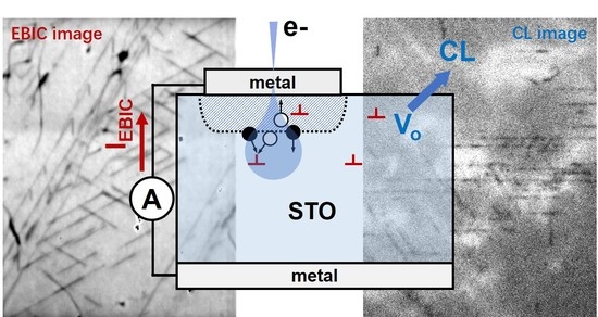
:
1. Introduction
2. Materials and Methods
3. Results and Discussion
4. Conclusions
Author Contributions
Funding
Acknowledgments
Conflicts of Interest
References
- Ang, C.; Yu, Z.; Cross, L.E. Oxygen-vacancy-related low-frequency dielectric relaxation and electrical conduction in Bi:SrTiO3. Phys. Rev. B 2000, 62, 228–236. [Google Scholar] [CrossRef] [Green Version]
- Ohtomo, A.; Hwang, H.Y. Growth mode control of the free carrier density in SrTiO3−δ films. J. Appl. Phys. 2007, 102, 083704. [Google Scholar] [CrossRef] [Green Version]
- Kalabukhov, A.; Gunnarsson, R.; Börjesson, J.; Olsson, E.; Claeson, T.; Winkler, D. Effect of oxygen vacancies in the SrTiO3 substrate on the electrical properties of the LaAlO3/SrTiO3 interface. Phys. Rev. B 2007, 75, 121404. [Google Scholar] [CrossRef] [Green Version]
- Siemons, W.; Koster, G.; Yamamoto, H.; Harrison, W.A.; Lucovsky, G.; Geballe, T.H.; Blank, D.H.; Beasley, M.R. Origin of charge density at LaAlO3 on SrTiO3 heterointerfaces: Possibility of intrinsic doping. Phys. Rev. Lett. 2007, 98, 196802. [Google Scholar] [CrossRef] [PubMed] [Green Version]
- Nian, Y.B.; Strozier, J.; Wu, N.J.; Chen, X.; Ignatiev, A. Evidence for an oxygen diffusion model for the electric pulse induced resistance change effect in transition-metal oxides. Phys. Rev. Lett. 2007, 98, 146403. [Google Scholar] [CrossRef] [Green Version]
- Janousch, M.; Meijer, G.I.; Staub, U.; Delley, B.; Karg, S.F.; Andreasson, B.P. Role of oxygen vacancies in Cr-doped SrTiO3 for resistance-change memory. Adv. Mater. 2007, 19, 2232–2235. [Google Scholar] [CrossRef] [Green Version]
- Yang, J.J.; Miao, F.; Pickett, M.D.; Ohlberg, D.A.A.; Stewart, D.R.; Lau, C.N.; Williams, R.S. The mechanism of electroforming of metal oxide memristive switches. Nanotechnology 2009, 20, 215201. [Google Scholar] [CrossRef] [Green Version]
- Fujii, T.; Kawasaki, M.; Sawa, A.; Kawazoe, Y.; Akoh, H.; Tokura, Y. Electrical properties and colossal electroresistance of heteroepitaxial SrRuO3/SrTi1−xNbxO3 (0.0002 ≤ x ≤ 0.02) Schottky junctions. Phys. Rev. B 2007, 75, 165101. [Google Scholar] [CrossRef]
- Li, J.Y.; Ohashi, N.; Okushi, H.; Haneda, H. Temperature dependence of carrier transport and resistance switching in Pt/SrTi1−xNbxO3 Schottky junctions. Phys. Rev. B 2011, 83, 125317. [Google Scholar] [CrossRef]
- Szot, K.; Speier, W.; Bihlmayer, G.; Waser, R. Switching the electrical resistance of individual dislocations in single-crystalline SrTiO3. Nat. Mater. 2006, 5, 312–320. [Google Scholar] [CrossRef]
- Sawa, A. Resistive switching in transition metal oxides. Mater. Today 2008, 11, 28–36. [Google Scholar] [CrossRef]
- De Souza, R.A.; Metlenko, V.; Park, D.; Weirich, T.E. Behavior of oxygen vacancies in single-crystal SrTiO3: Equilibrium distribution and diffusion kinetics. Phys. Rev. B 2012, 85, 174109. [Google Scholar] [CrossRef]
- Marrocchelli, D.; Sun, L.; Yildiz, B. Dislocations in SrTiO3: Easy to reduce but not so fast for oxygen transport. J. Am. Chem. Soc. 2015, 137, 4735–4748. [Google Scholar] [CrossRef] [PubMed]
- Jiang, W.; Evans, D.; Bain, J.A.; Skowronski, M.; Salvador, P.A. Electron beam induced current investigations of Pt/SrTiO3−x interface exposed to chemical and electrical stresses. Appl. Phys. Lett. 2010, 96, 092102. [Google Scholar] [CrossRef]
- Chen, J.; Sekiguchi, T.; Li, J.Y.; Ito, S.; Yi, W.; Ogura, A. Investigation of dislocations in Nb-doped SrTiO3 by electron-beam-induced current and transmission electron microscopy. Appl. Phys. Lett. 2015, 106, 102109. [Google Scholar] [CrossRef]
- Chen, J.; Sekiguchi, T.; Li, J.Y.; Ito, S. Investigation of dislocations in Nb-doped (100) SrTiO3 single crystals and their impacts on resistive switching. Superlattices Microstruct. 2016, 99, 182–185. [Google Scholar] [CrossRef]
- Kan, D.; Terashima, T.; Kanda, R.; Masuno, A.; Tanaka, K.; Chu, S.; Kan, H.; Ishizumi, A.; Kanemitsu, Y.; Shimakawa, Y.; et al. Blue-light emission at room temperature from Ar+-irradiated SrTiO3. Nat. Mater. 2005, 4, 816–819. [Google Scholar] [CrossRef]
- Bruno, F.Y.; Tornos, J.; Olmo, M.G.; Santolino, G.S.; Nemes, N.M.; Garcia-Hernandez, M.; Mendez, B.; Piqueras, J.; Antorrena, G.; Morellon, L.; et al. Anisotropic magnetotransport in SrTiO3 surface electron gases generated by Ar+ irradiation. Phys. Rev. B 2011, 83, 245120. [Google Scholar] [CrossRef] [Green Version]
- Lim, J.; Lee, Y.S.; Bu, S.D. Surface-direction dependence of the oxygen vacancy formation in SrTiO3 single crystals. Ceram. Int. 2018, 44, S93–S95. [Google Scholar] [CrossRef]
- Lee, D.; Wang, H.W.; Noesges, B.A.; Asel, T.J.; Pan, J.B.; Lee, J.W.; Yan, Q.; Brillson, L.J.; Wu, X.; Eom, C.B. Identification of a functional point defect in SrTiO3. Phys. Rev. Mater. 2018, 2, 060403(R). [Google Scholar] [CrossRef]
- Wang, P.; Yi, W.; Chen, J.; Ito, S.; Cui, C.; Sekiguchi, T. Oxygen vacancy migration along dislocations in SrTiO3 by cathodoluminescence. J. Phys. D Appl. Phys. 2019, 52, 475103. [Google Scholar] [CrossRef]
- Shockley, W.; Read, W.T. Statistics of the recombination of holes and electrons. Phys. Rev. 1952, 87, 835–842. [Google Scholar] [CrossRef]
- Kusanagi, S.; Sekiguchi, T.; Shen, B.; Sumino, K. Electrical activity of extended defects and gettering of metallic impurities in silicon. Mater. Sci. Technol. 1995, 11, 685–690. [Google Scholar] [CrossRef]
- Kveder, V.; Kittler, M.; Schröter, W. Recombination activity of contaminated dislocations in silicon: A model describing electron-beam-induced current contrast behavior. Phys. Rev. B 2001, 63, 115208. [Google Scholar] [CrossRef]
- Chen, J.; Sekiguchi, T.; Yang, D.; Yin, F.; Kido, K.; Tsurekawa, S. Electron-beam-induced current study of grain boundaries in multicrystalline silicon. J. Appl. Phys. 2004, 96, 5490–5495. [Google Scholar] [CrossRef]
- Kittler, M.; Seifert, W. Two types of electron-beam-induced current behaviour of misfit dislocations in Si(Ge): Experimental observations and modelling. Mater. Sci. Eng. B 1994, 24, 78–81. [Google Scholar] [CrossRef]
- Maximenko, S.I.; Freitas, J.A., Jr.; Myers-Ward, R.L.; Lew, K.-K.; VanMil, B.L.; Eddy, C.R., Jr.; Gaskill, D.K.; Muzykov, P.G.; Sudarshan, T.S. Effect of threading screw and edge dislocations on transport properties of 4H–SiC homoepitaxial layers. J. Appl. Phys. 2010, 108, 013708. [Google Scholar] [CrossRef] [Green Version]
- Chan, N.-H.; Sharma, R.K.; Smyth, D.M. Nonstoichiometry in SrTiO3. J. Electrochem. Soc. 1981, 128, 1762–1769. [Google Scholar] [CrossRef]


© 2020 by the authors. Licensee MDPI, Basel, Switzerland. This article is an open access article distributed under the terms and conditions of the Creative Commons Attribution (CC BY) license (http://creativecommons.org/licenses/by/4.0/).
Share and Cite
Yi, W.; Chen, J.; Sekiguchi, T. Electron-Beam-Induced Current and Cathodoluminescence Study of Dislocations in SrTiO3. Crystals 2020, 10, 736. https://doi.org/10.3390/cryst10090736
Yi W, Chen J, Sekiguchi T. Electron-Beam-Induced Current and Cathodoluminescence Study of Dislocations in SrTiO3. Crystals. 2020; 10(9):736. https://doi.org/10.3390/cryst10090736
Chicago/Turabian StyleYi, Wei, Jun Chen, and Takashi Sekiguchi. 2020. "Electron-Beam-Induced Current and Cathodoluminescence Study of Dislocations in SrTiO3" Crystals 10, no. 9: 736. https://doi.org/10.3390/cryst10090736