Article

Microwave Irradiation to Produce High Performance Thermoelectric Material Based on Al Doped ZnO Nanostructures

1
Center of Nanotechnology, King Abdulaziz University, Jeddah 21589, Saudi Arabia
2
Department of Physics, Faculty of Science, King Abdulaziz University, Jeddah 21589, Saudi Arabia
3
Nagoya Industrial Science Research Institute, Nagoya 464-0819, Japan
4
Department of Applied Physics, Kyung Hee University, Yong-in 17104, Korea
*
Authors to whom correspondence should be addressed.
Crystals 2020, 10(7), 610; https://doi.org/10.3390/cryst10070610
Submission received: 12 June 2020 / Revised: 4 July 2020 / Accepted: 6 July 2020 / Published: 13 July 2020
(This article belongs to the Special Issue Zinc Oxide Nanomaterials and Based Devices)

Abstract

:
Microwave irradiation is found to be effective to provide highly crystalline nanostructured materials. In this work, this technique has been used to produce highly improved thermoelectric (TE) material based on aluminum (Al) doped zinc oxide (ZnO) nanostructures (NSs). The effect of Al dopant at the concentration range 0.5–3 mol % on the structural and TE properties has been investigated in more details. The optimum concentration of Al for better TE performance is found to be 2 mol %, which could significantly increase the electrical conductivity and reduce the thermal conductivity of ZnO NSs and thus enhance the TE performance. This concentration showed almost metallic conductivity behavior for ZnO NSs at low temperatures, e.g., below 500 K. The electrical conductivity reached 400 S/m at room temperature, which is around 200 times greater than the value recorded for the pure ZnO NSs. Remarkably, the measured room temperature thermal conductivity of the microwave synthesized ZnO NSs was very low, which is around 4 W/m·K. This value was further reduced to 0.5 W/m·K by increasing the Al doping to 3 mol %. The figure of merit recorded 0.028 at 675 K, which is 15 times higher than that of the pure ZnO NSs. The output power of a single leg module made of 2 mol % Al doped ZnO NSs was 3.7 µW at 485 K, which is higher by 8 times than that of the pure sample. These results demonstrated the advantage of the microwave irradiation rout as a superior synthetic technique for producing and doping promising TE nanomaterials like ZnO NSs.

1. Introduction

Thermoelectricity is the direct conversion of heat to electricity generated from a temperature gradient occurring in thermoelectric materials. Since thermoelectricity can exploit waste heat and it does not generate deleterious by-products, it offers potential for use in next-generation green energy techniques. However, the thermoelectric property of thermoelectric devices is limited, curbing their commercial applications. Thermoelectric property is defined as a figure of merit (zT) expressed as S2σT/κ, (S: Seebeck coefficient, σ: electric conductivity, κ: thermal conductivity, T: absolute temperature). Effective thermoelectricity requires low thermal conductivity and high electrical conductivity and Seebeck coefficient. Thus, it is evident that the thermal and electrical parameters need to be optimized to improve the thermoelectric properties [1]. The materials needed for potential applications used in thermoelectric materials include being made from naturally abundant elements, having high chemical and thermal stability, and being nontoxic. These represent the main advantages of oxide-based TE materials over traditional thermoelectric materials [2]. Over the past twenty years, the zT of oxides have been improved considerably [3]. One of them is zinc oxide (ZnO), which has a wide band gap (3.4 eV) semiconductor, with a potential application in optical and electrical devices, such as TE materials [4]. Due to the presence of native defects in the ZnO lattice, un-doped ZnO exhibits n-type conductivity [5]. The electrical, magnetic, optical, and thermal properties of ZnO are enhanced by generating extra electrons e.g., by substituting Zn2+ ions with group III ions such as aluminum. Due to being an abundant, low-cost material with a small ionic radius, Al is the dopant element used most commonly [6].
The doping procedure has a significant effect on electrical conductivity, which can be selectively increased by improving the carrier concentration via dopant structural integration into the host lattice arrangement process [6]. There are a number of methods by which ZnO can be synthesized, including atomic layer deposition [7], pulsed laser deposition [8], sputtering [9], and the sol–gel method [10]. Incorporating dopant elements from group III, such as Al, into the ZnO structure leads to an enhancement in electrical and optical properties [6]. Furthermore, Al incorporation into ZnO lattice causes lattice shrinking owing to the difference between the ionic radii of Al (0.054 nm) and Zn (0.074 nm) [11]. However, the procedure of dopant incorporation into the ZnO lattice is considered as a key factor in dictating the output TE properties due to the importance of dopant molecules engagements on the ZnO plane distances. This was reported to lead to Al incoropration effect within the ZnO lattice, which that has a direct control on electron and phonon diffusion across the sample [11]. Keeping these factors in mind, it is of great importance to find out an affective methodology to produce high performance TE materials.
Here, we investigate the use of microwave irradiation method for producing pure and Al doped ZnO nanostructures. Generally, the procedure of element doping has a significant effect on thermoelectric properties, the microwave irradiation assisted method has unique features—such as rapid heating, while being simple, fast, and economical—and it is an effective method for providing highly crystalline materials [12]. Moreover, it is expected that incorporating the Al molecules into the ZnO lattice perfectly might significantly enhance the thermoelectric properties of ZnO. Therefore, this work is designed to produce pure and Al doped ZnO NSs at different concentrations (0.5, 1, 2 and 3 mol %) and study their structural and TE properties. The sample characterizations were divided into three measures, firstly, structural properties of the samples were determined in order to study the integration of the Al into ZnO lattice using a range of analysis techniques such as SEM, EDX, Mapping EDX, HRTEM, FTIR, Raman spectroscopy, and XPS to figure out a comprehensive investigation of the effectiveness of microwave irradiation method in doping Al within ZnO structure. Secondly, the thermoelectric properties of the samples were studies for evaluating the efficiency of Al doping in enhancing the TE properties and the optimal Al concentration was determined, finally, a single leg TE module was designed and tested for its power output as a function of temperature in order to explore the influence of Al doping for improving the TE performance for future TE devices.

2. Materials and Methods

The ZnO nanomaterials were synthesized using the previously described method [12]. The microwave irradiation system of Milestone, Italy, was used. The reagents obtained in this experiment are of analytical grade (99.99%) and were purchased from Sigma Aldrich. Therefore, no modification or further purification was required. ZnO nanostructures were synthesized using Zn(NO3)2·6H2O and hexamethylenetetramine (HMT) (C6H12N4), in a molar ratio of 3:20. Briefly, 5 g of Zn(NO3)2·6H2O and 15.7 g of C6H12N4 were used along with the desired concentrations of Al(NO3)3 which are 0.5, 1, 2, and 3 mol %. The mixtures were dissolved in 50 mL deionized water and stirred for 30 min until solutes had completely dissolved. Solutions were exposed to microwave irradiation at 750 W (~120 °C) for 10 min with magnetic stirring and the reaction temperature reached around 120 °C after 10 min of the reaction. The samples were then centrifuged to isolate the precipitate. The precipitates were washed several times with deionized water and absolute ethanol. Then the obtained materials were dried in an oven for 24 h at 80 °C.
The above synthesized ZnO samples were analyzed using An ULTIMA IV X-ray diffractometer (XRD) (Rigaku, Japan) using Cu Ka radiation (k = 1.5406 Å). The XRD data were extracted through Rigaku data analysis software (Rigaku, PDXL2, version 2, Tokyo, Japan). The produced nanostructures morphology and microstructure were analyzed by field scanning electron microscopy (SEM) (JEOL, JSM-7500F model, Tokyo, Japan) and transmission electron microscopy (TEM) (JEOL, JEM 2100F model, Tokyo, Japan). Raman spectra were recorded using Micro Raman system; model DXR, Thermo Fisher Scientific, Waltham, MA, USA. They were recorded using a 532 nm laser and 7 mW power. Attenuated total reflection-Fourier-transform infrared (ATR-FTIR) spectrometry (Thermo Fisher Scientific, Waltham, MA, USA) was used to obtain FTIR spectra; the wavelength range used was 400–4000 cm−1 with 0.5 cm−1 resolution. A PHI 5000 VersaProbe (Chigasaki, Kanagawa, Japan) device was used to collect X-ray photoelectron spectroscopy (XPS) measurements. A manual hydraulic press was used to create the pellets measuring 13 mm in diameter and 0.5–2 mm thickness under pressure of 5 Tons for 15 min. Evaluation of Seebeck coefficient and electrical conductivity were performed using the LSR-3 Linseis-Seebeck coefficient and electric resistivity system, Linseis, Germany under a helium gas atmosphere. Thermal conductivity was measured using a Laser Flash Thermal Conductivity Analyzer (LFA-1000, Linseis, Selb, Germany) that was perpendicular to the pellet surface. The heating rate and temperature gradient between the hot and cold sides were fixed at 5 K/min and 323 K, respectively.

3. Results and Discussion

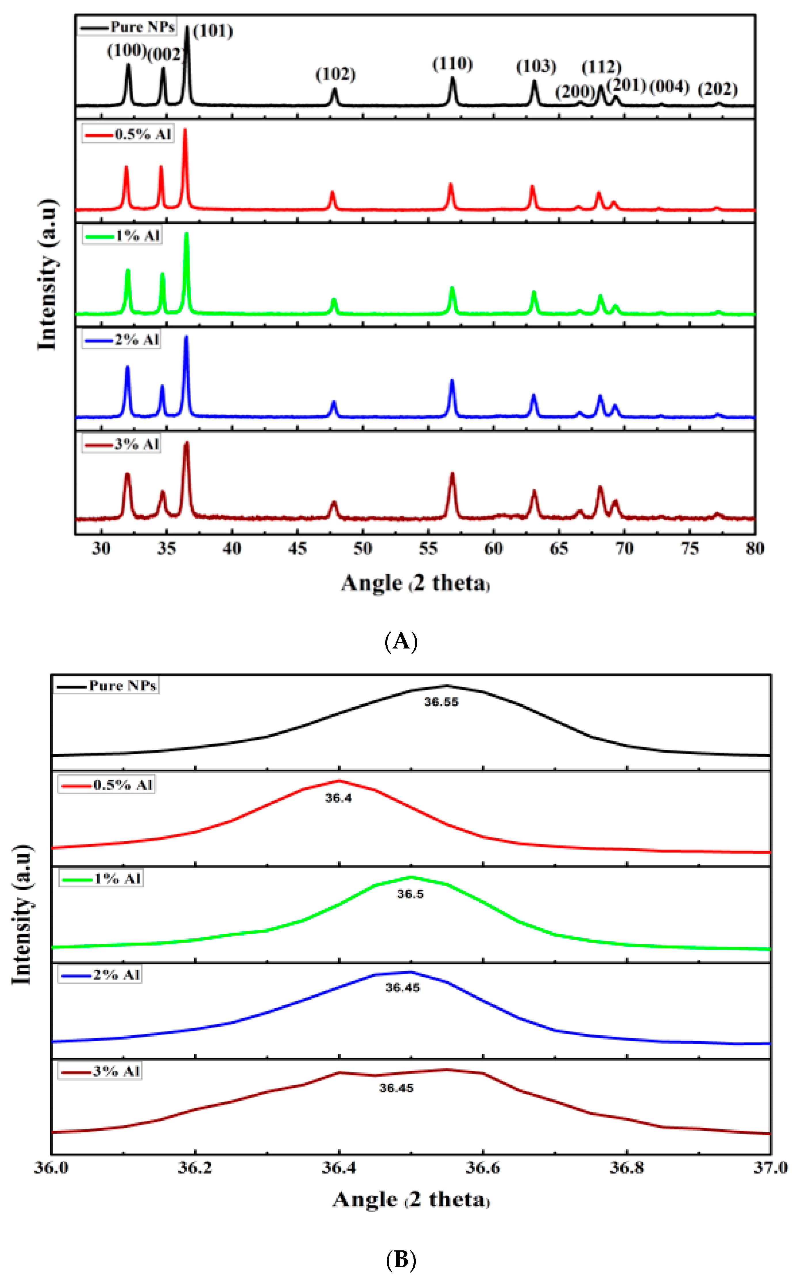
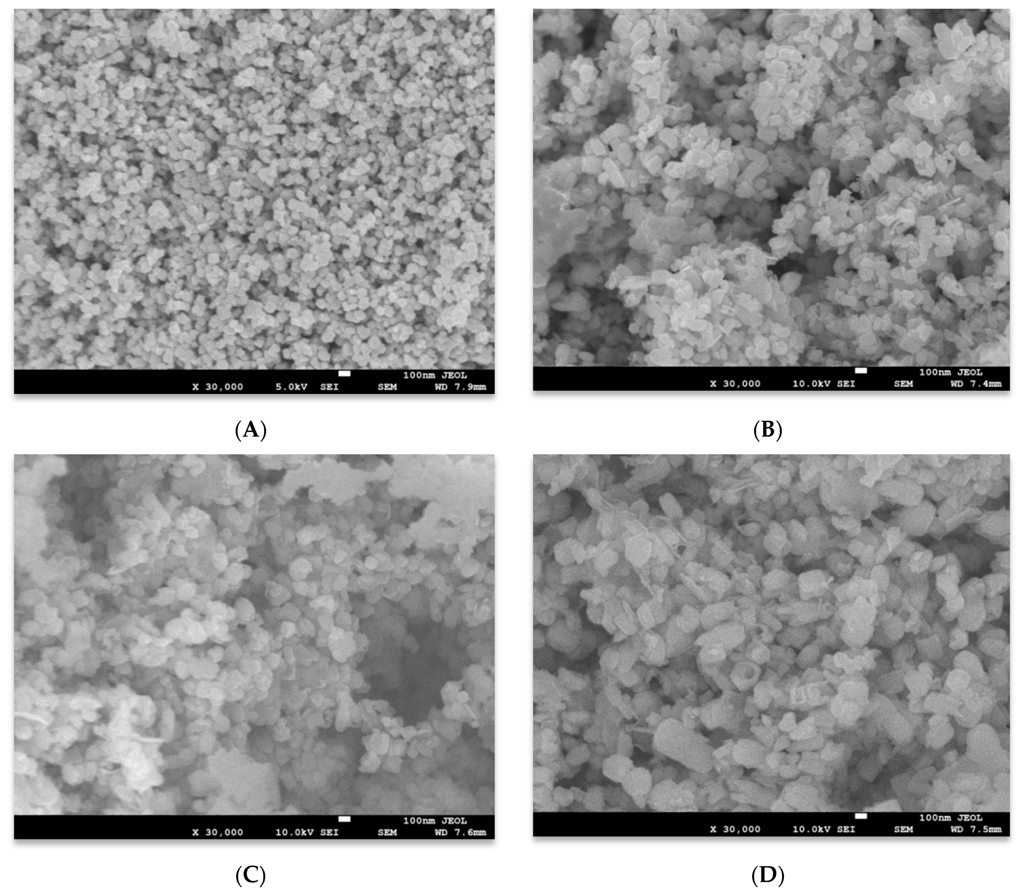
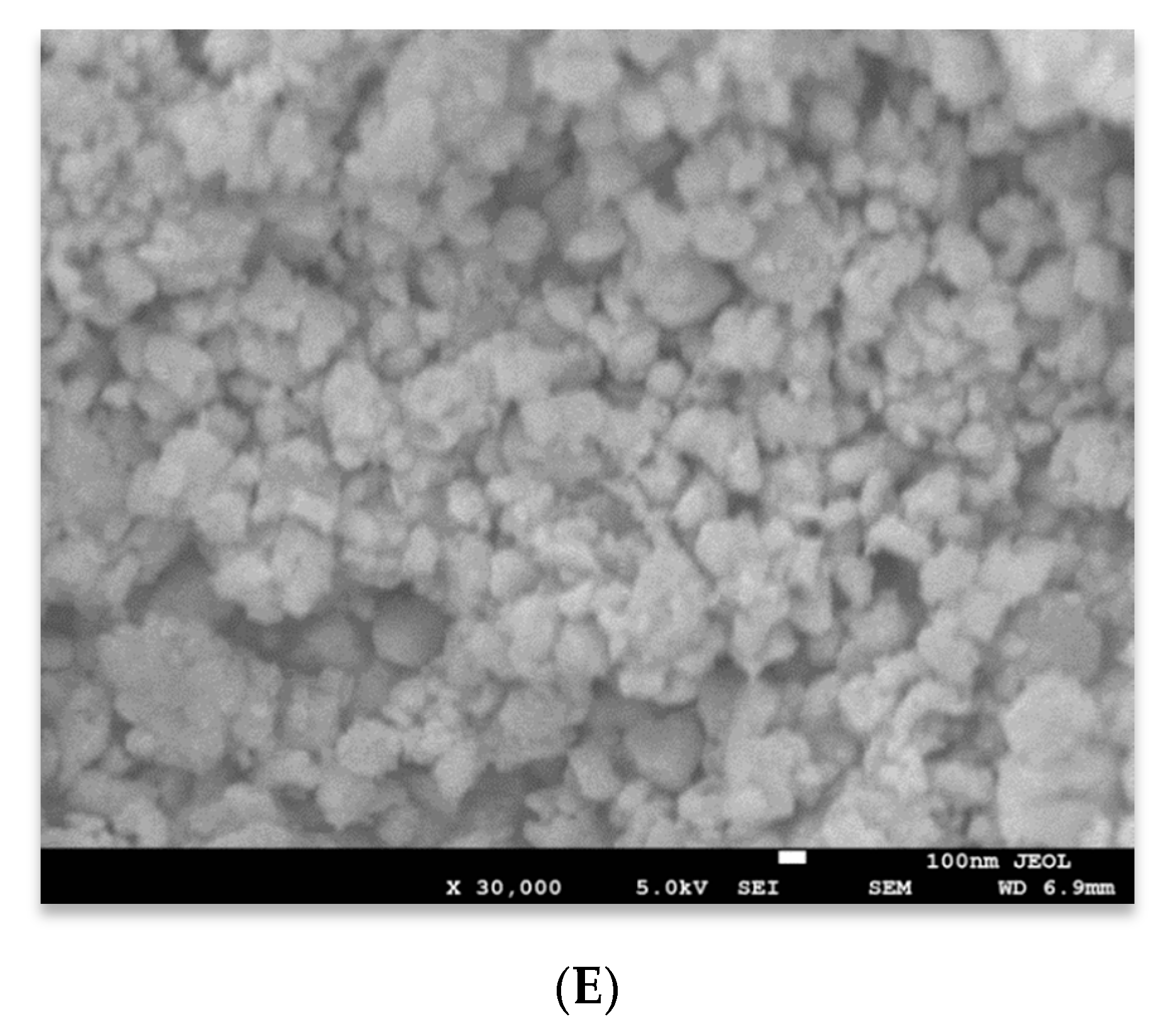
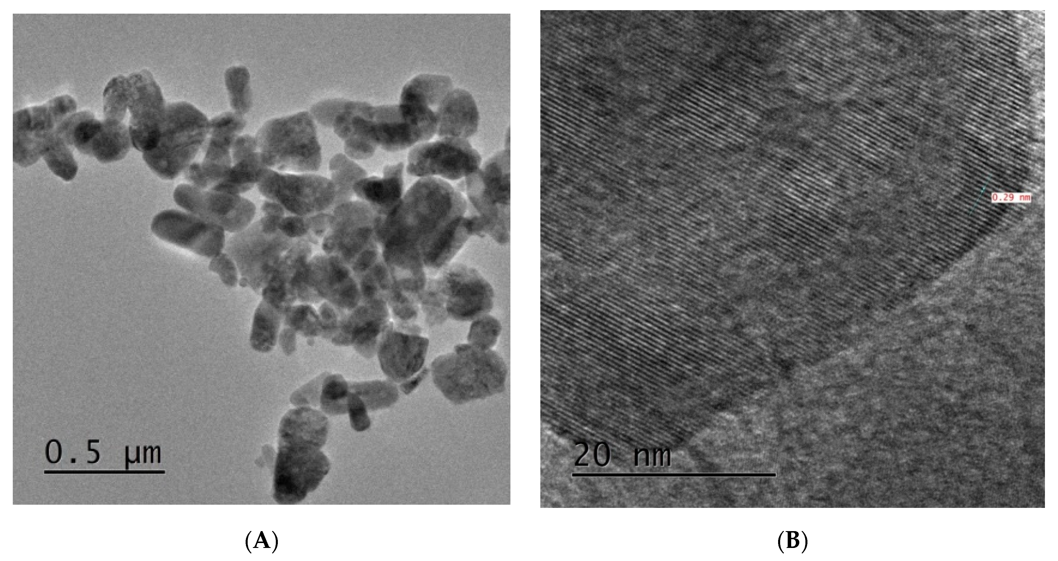
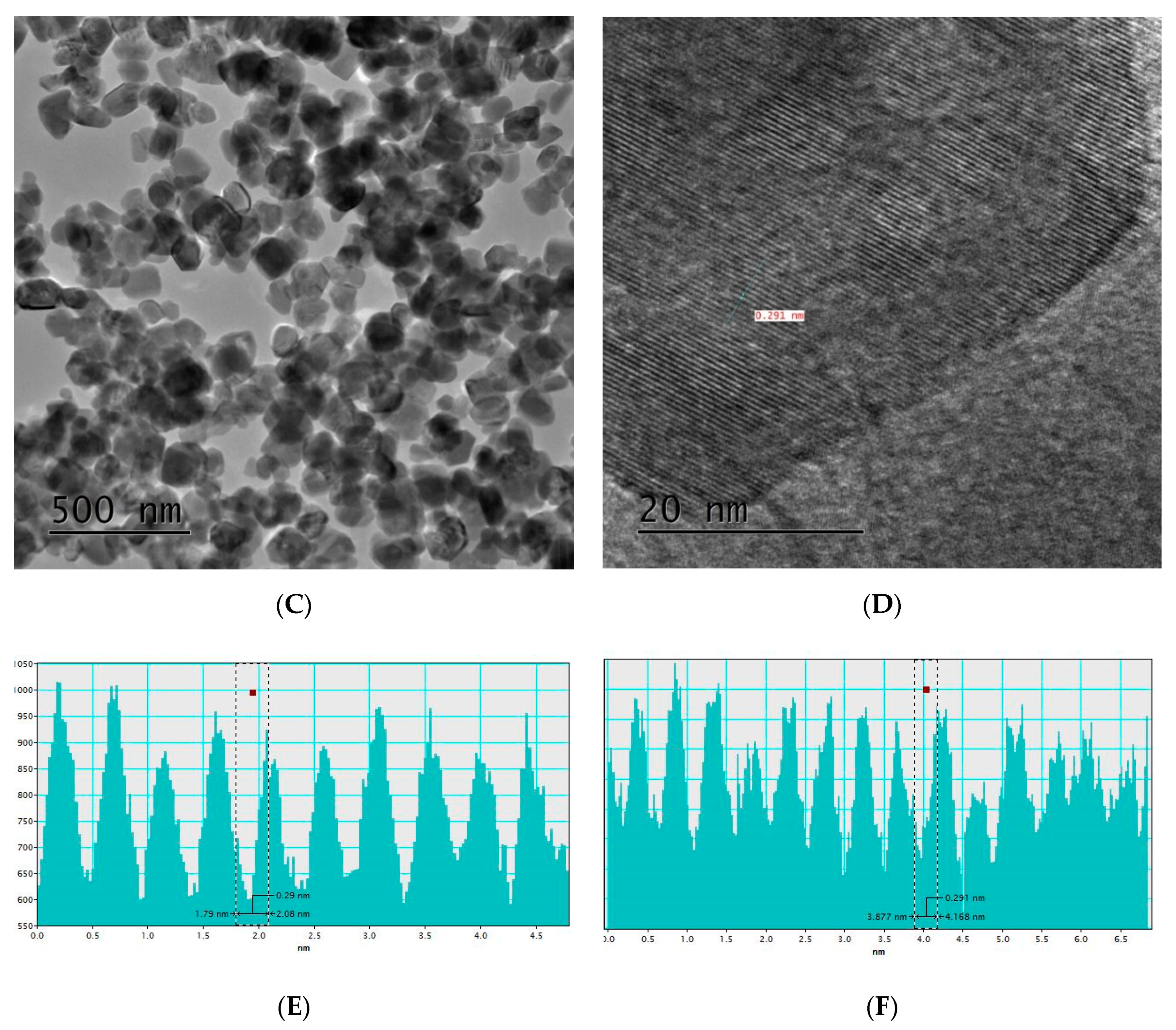
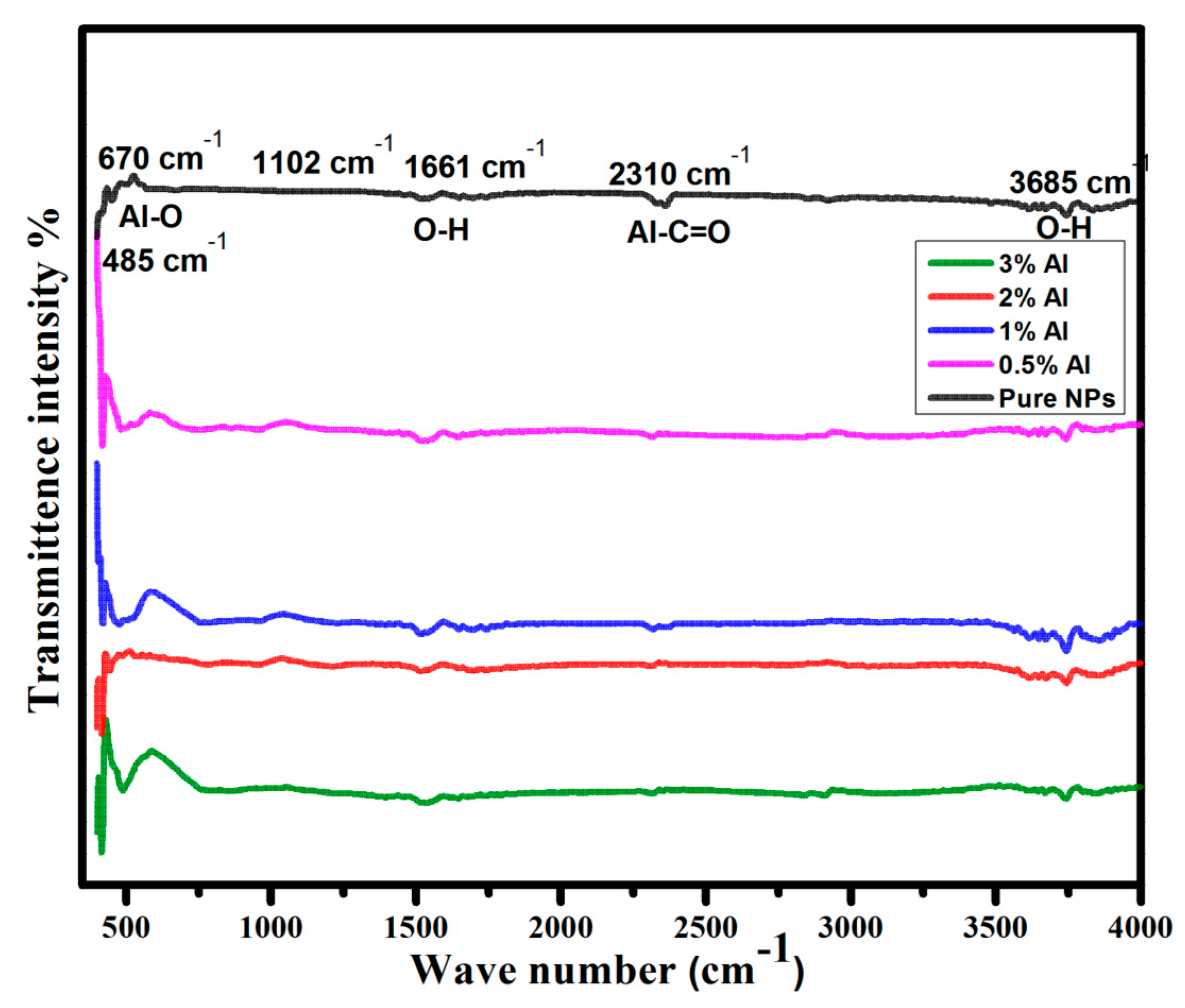
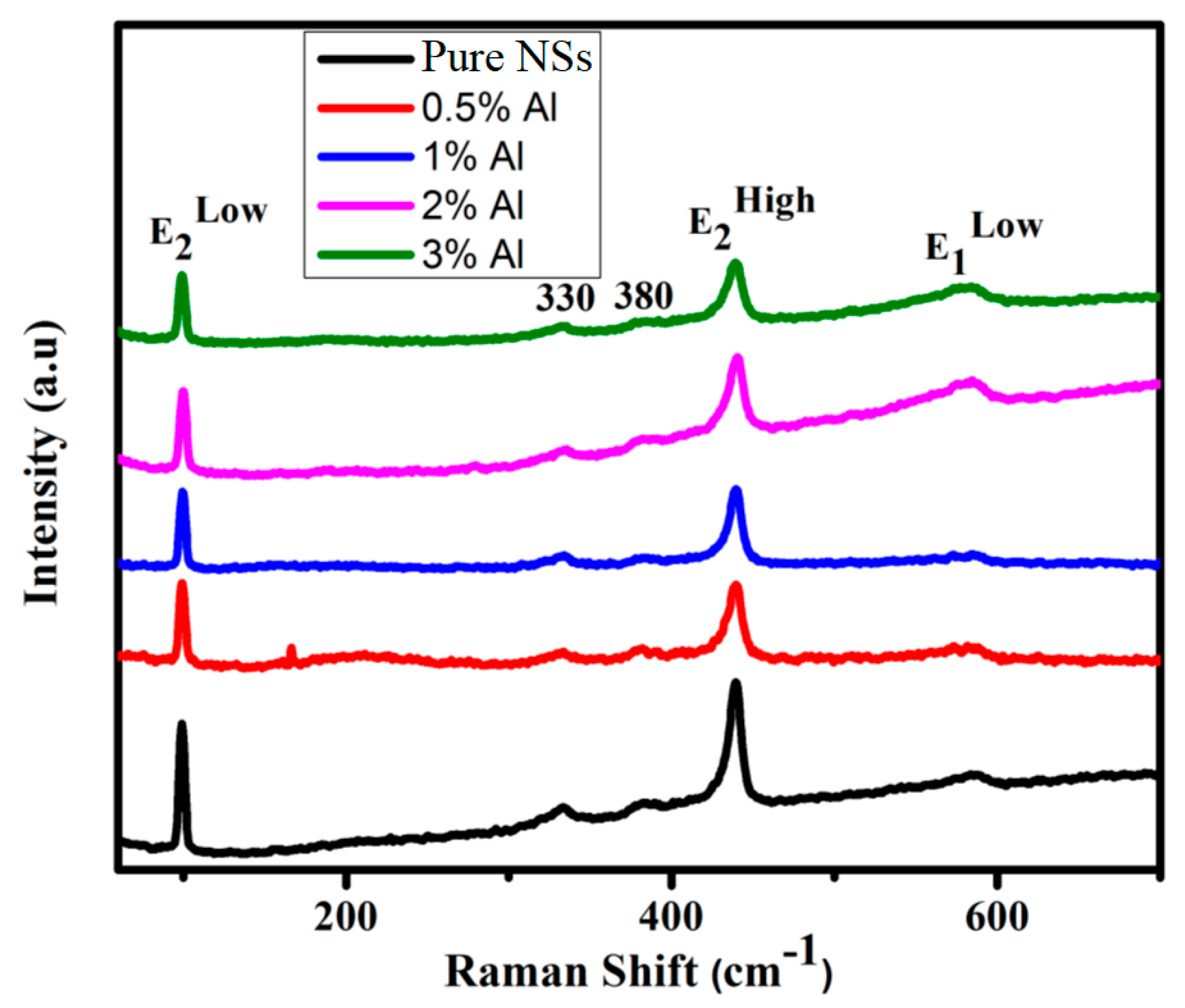
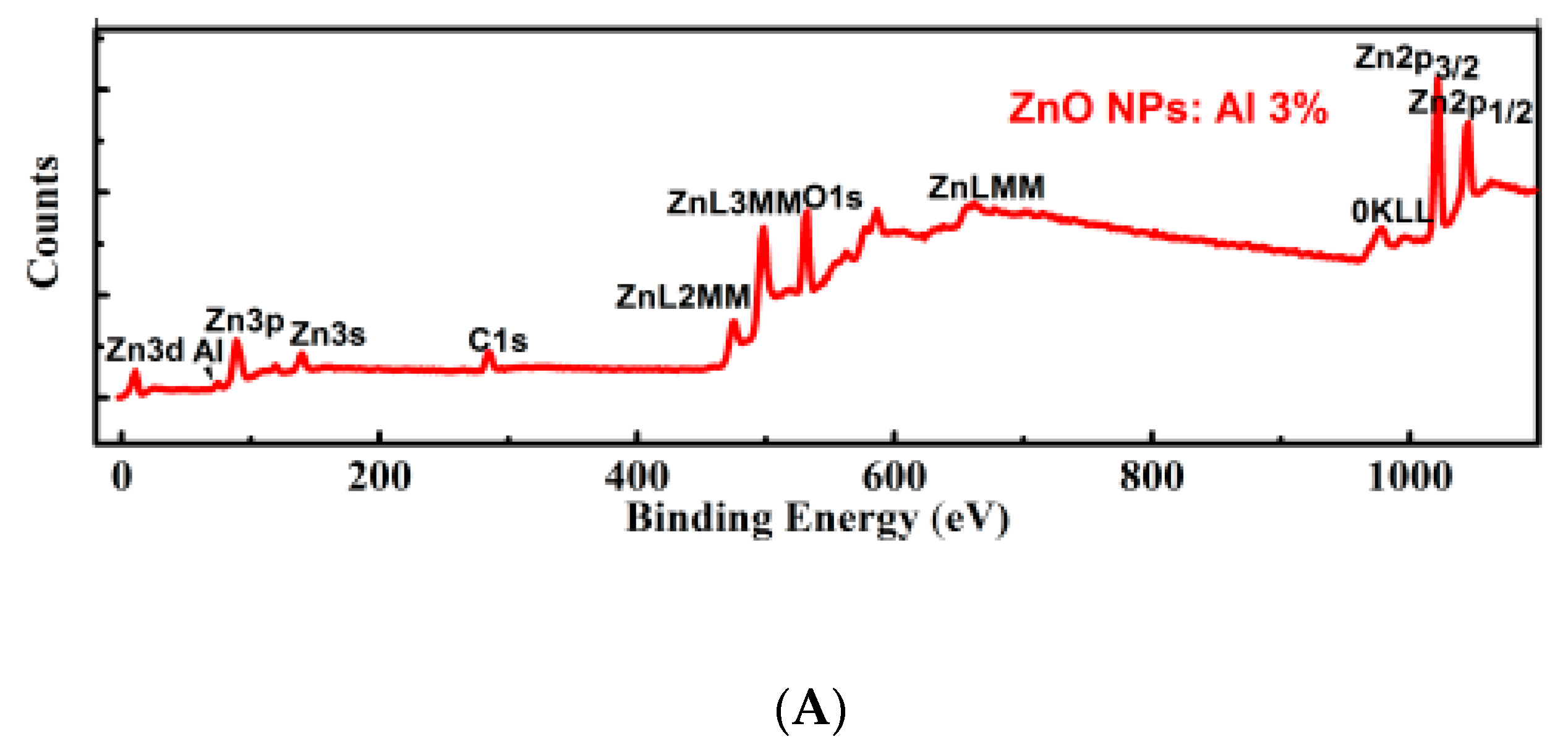
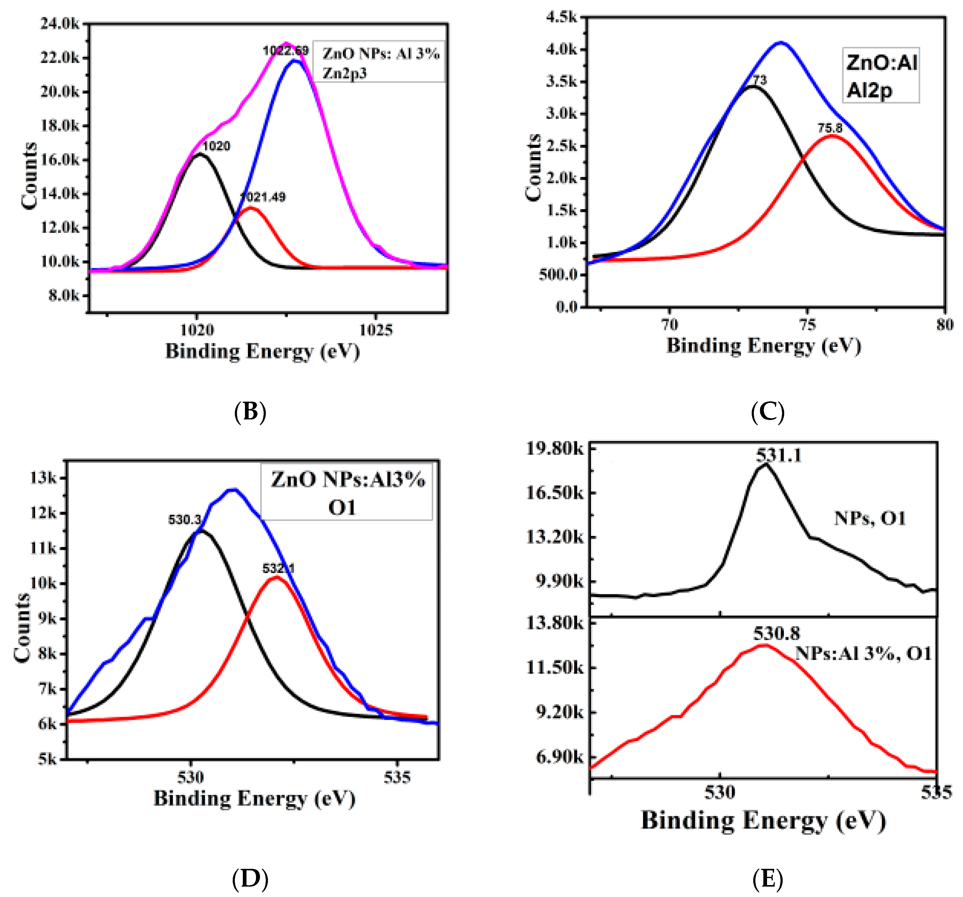
3.1. Structural Properties

The phase and crystalline structure of the material were studied using XRD. The obtained results of the pure and Al doped ZnO NSs are shown in Figure 1A. All the samples exhibit the same hexagonal wurtzite structure (JCPDS 36–1451). However, only ZnO peaks were detected by XRD; no permanent or detectable peaks belong to aluminum and its components. This might be due to the amount of Al content, which is low and completely incorporated in the ZnO lattice, making it difficult to detect. It atomically distributed within the ZnO lattice or isolated to the grain boundaries of the ZnO nanocrystals. The peaks of the miller indices (002) and (101) show peak diffraction angles at 33.4° and 36.2°, with lower and broader peaks intensities in the Al doped samples. This might be attributed to the reduced crystallites sizes caused by Al incorporation. Figure 1B demonstrates a zoomed area of plane (1, 0, 0) in order to investigate the effect of Al dopant on that plane position, intensity, and broadening. It is clear that the dopant provides a slight shift in positions and the mostly doped sample (Al 3%) shows most broader peak and lowest intensity. Due to the Al dopant engagement indicated by the lattice’s constant parameter (a and c), confirming that Al dopant inhibited grain growth (Table 1) [11]. This phenomenon was demonstrated by a reduction in lattice constants of (a) and (c) (Table 1) [13,14]. However, the slight change in the lattice parameter ratio (c/a) and small shift indicates that uniform strain is induced in the structure [15]. It can be observed in Table 1 that the lattice constant c are reduced after Al doping, but the lattice constant ratio c/a of the un-doped ZnO is similar to that of the 2 mol % Al doped sample, which representing that this concentration is perfectly fitting the ZnO hexagonal planes leaving no extra, vacant, or unfilled sites. The dopant concentration e.g., 2 mol % is perhaps the most energetically stable configuration for a given hexagonal structure. Additional doping level above 2 mol % Al, e.g., the excessive aluminum content was reported to produce ZnAl2O4 spinel phase [16]. This phase cause electron carriers being blocked and scattering of transferred electrons, affecting the material’s thermoelectric properties [17]. The present result is also close to that reported by Shirouzu et al. [18], who reported that the Al distribution and maximum solubility limit in ZnO is achieved at 3 at%. Interim of electrical conductivity it was reported that by increasing Al doping, there is a concomitant increase in electrical conductivity [19], which has been attributed to the rise in the number of freed electrons and inhabitation of the grain growth.
The SEM and TEM techniques were used to examine the morphology of the generated pure and Al-doped ZnO materials. The obtained results are presented in Figure 2 and Figure 3. Figure 2A, shows that the morphology of the pure ZnO, which comprised a mixture of uniform and random nanoparticles. These nanostructures have particle size within the range 20–50 nm. In the Al doped ZnO samples, slight distractions on the shape of these nanoparticles can be observed as shown in Figure 2B–E. This is evidence that incorporating aluminum into ZnO influences ZnO morphology, with uniform solid nanoparticles being converted into random shape nanostructures. As mentioned above, the Al dopant could induce a slight change in the lattice parameter c, which might generate non-uniform strain on the formed structures during their growth [15].
Figure 3A shows TEM image for the pure ZnO NSs. The nanoparticles shown in this image are similar to those presented in the SEM image (Figure 2A). A mixture of small and big nanoparticles within the range 25–60 nm can be observed. The HRTEM image of the pure ZnO NSs given in Figure 3B shows single crystalline structures. This is a remarkable result, which is a property of the microwave chemical assisted rout to provide highly crystalline structures mostly in a single nanocrystal form [12]. In the case of the Al doped sample (of 3 mol % Al doped-ZnO NSs), the TEM image in Figure 3C, shows almost similar shapes to those of the pure ZnO NSs with slight smaller sizes, but the HRTEM image given in Figure 3D shows almost polycrystalline structures. The TEM-determined dimensions are slightly larger than those determined by SEM (Figure 2D,E). The d-spacing values are identical in doped and un-doped samples. It is around 0.29 nm for the pure ZnO NSs (Figure 3E) and 3 mol % Al doped sample (Figure 3F). These findings are in agreement with the XRD results d-spacing of phase plane (1, 0, 0).
Elemental analysis of Al doped ZnO (3 mol %) was conducted by SEM-EDS m and color mapping analysis. The results presented in Figure 4A–E confirmed the existence of Zn, O, and Al elements, which are uniformly distributed across the sample particles. The EDS analysis revealed precipitates to be Al, Zn, and O rich (Figure 4A). The EDS mapping pattern also confirms the existence of all expected elemental compositions (Zn, O, and Al shown in Figure 4B, Figure 4C, and Figure 4D, respectively). The mapping image (Figure 4C) showing that the Al has been distributes equally across the whole sample particles, which confirm the perfect solubility of the Al dopant within the reaction. In addition, it confirms the optimized Al intake by absorbing only 2.2% percentage by atomic weight of the Al within the ZnO host, whereas the practical Al percentage was 3 mol %, see Table 2. This reflects that there is small unreacted excess Al in the reaction, which may affect the output thermoelectric performance. This result is with agreement with the XRD lattice constant parameter that demonstrating the c/a of pure and Al 2 mol % are identical, indicating the optimum Al concentration at around 2 mol %.
Figure 5 shows the FTIR spectra of pure and Al doped ZnO NSs. Spectra of the NSs doped with various concentrations (0.5, 1, 2, and 3 mol %) are shown in the range 400–4000 cm−1. The broad absorption band at 3680 cm−1 and 1660 cm−1 can be ascribed to O–H bending vibration of water molecules absorbed in the whole range of ZnO nanostructure [20]. The peak at 2310 cm−1 is attributed to CO2 absorption in pure ZnO. The intensity of this peak is reduced after the formation of Al–C=O+ by the metal oxide bond absorption belong to Al metal dopant. It has been shown that there is an intensity of 2310 cm−1 decreased correlated to Al doping content increased, which signifies the bond strength between the dopant and ZnO changed [21]. The peak at 674 cm−1 might be ascribed to Al-O, which indicates that the intensity and broadening of the peaks increased as Al doping increased, except that of 2 mol % (might be due to the non-standby amount of Al dopant). The sharp peak at 498 cm−1 might be assigned to Zn–O [22].
Raman spectroscopy analysis is a powerful tool to study the crystal quality, and structural defects and disorders. The Raman-active optical phonon modes, which classified as A1+E1 + 2E2, can be observed in Figure 6. They are characteristic of wurtzite structures of ZnO. Three major peaks that appear in the spectrum of pure ZnO are located at 380 cm−1 (A1 mode), 437 cm−1 (E2 mode), and 548 cm−1 (E1 mode). The latter is recognized as being a multi-phonon response [23,24]. The small peak at 330 cm−1 is ascribed to a second order nonpolar 2E2 mode. Typically, there are no additional peaks when Al dopant is incorporated in ZnO host. The sharpness and broadening of the E2 peak, which is characteristic of the wurtzite structure, ZnO indicates the highly crystalline of the formed grains/crystals. Therefore, it can be observed that the peaks sharpness was reduced (becoming broader) and the intensities were increased according to the increase in Al content in the samples. Thus, higher Al incorporation into ZnO lattice showed broader E2 peaks and higher intensities are also observed. The peak intensity of E2 (high and low) mode is found to decrease as the Al concentration increases [23].
The distribution and chemical state of the elements forming the pure and Al-doped ZnO were analyzed using XPS (Figure 7A–E). The survey scan shows that there are no other impurities were identified in the Al doped sample, only C, Zn, O, and Al are detected (Figure 7A). Figure 7B shows the Zn 2p pattern of the Al doped ZnO NSs. Binding energy peak was observed at 1022.7 eV, which corresponds to the spin orbit of Zn 2p3/2, indicative of a divalent chemical state in the sample [25]. The signal at 1020 eV observed in the Al doped ZnO NSs indicates that the Zn is in the oxidized state [26,27]. The peak of 530.4 ± 0.1 eV shown in Figure 7D for the Al doped sample is attributed to the oxygen in the lattice being bound as O2− ions, which could be decomposed into two peaks [28,29]. These two peaks might be related to the ZnO and Al2O3/AlO(OH) phases [26]. The binding energy peak at 74.7 eV in Figure 7C corresponds to Al 2p. This confirms that Al could successfully incorporate in its 3+ chemical state into the Zn2p sites of ZnO [30]. The XPS spectrum of the Al 2p core level was deconvolved into two components. The low bonding energy component centred at 73 eV might be due to the peak position of stoichiometric Al2O3 [31], and similarly the component at 75.8 eV may be due to the AlO(OH) [26]. Figure 7E shows the peak position of O1s in both pure and Al doped ZnO NSs samples. Clear shifting to the low binding energy side can be seen due to Al doping, which might be due to the bonding with different phases such as Al2O3/AlO(OH) [26].

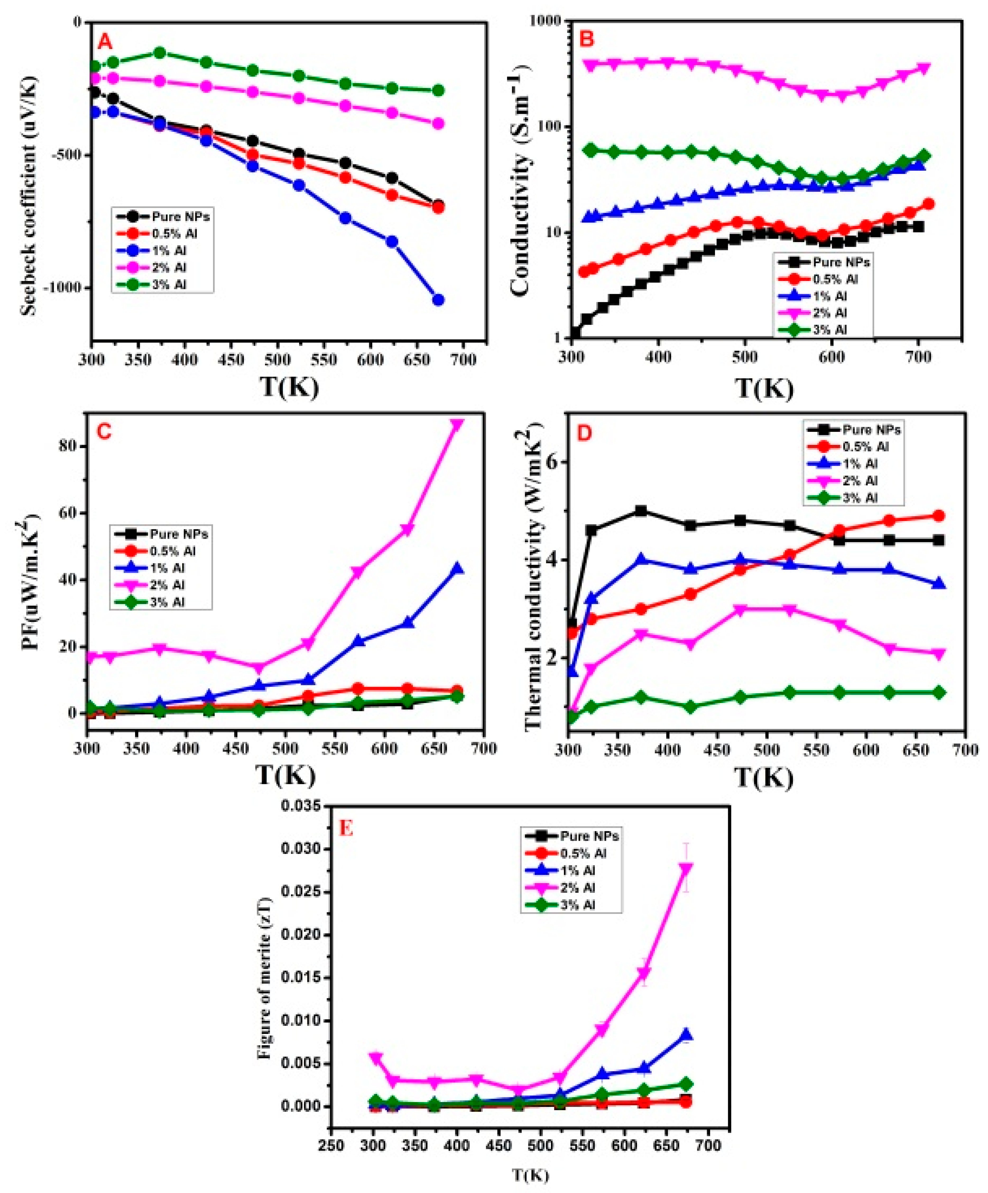
3.2. Thermoelectric Properties

The ultimate aim of this work is to study the TE properties of Al doped ZnO NSs produced by the microwave irradiation method. Figure 8 shows the obtained TE results as a function of temperature. The first parameter is the Seebeck coefficient (Figure 8A), where the obtained values of the pure and Al doped ZnO NSs are plotted. It is clear that the pure and doped samples returned a negative Seebeck coefficient, with absolute values increasing concomitantly with temperature. This indicates the character of the ZnO NSs to be as usual n-type semiconductor, which was consistent with expectations. The doped samples are also found to be n-type semiconductors, but might be with higher carrier concentrations [32]. At low concentrations of Al dopant, the Seeback coefficient values were slightly increased. However, when Al concentration increases above 1 mol %, e.g., up to 2 and 3 mol %, the Seebeck coefficient is significantly decreased. This might be due to the increase in number of free electrons that might saturated at which supposed that the excess Al did not fully dissolve in the ZnO lattice during reaction synthesis, which in turn hugely effects the Seebeck coefficient. Nevertheless, it is worth mentioning that the microwave synthesized ZnO NSs have provided the highest Seebeck coefficient value, which has not been reported earlier on ZnO by any other synthesis technique. The Seeback coefficient value reached −1022 μV/K for the 1 mol % Al doped ZnO NSs at a temperature of 675 K. This value is remarkably high compared to other techniques including spray pyrolysis [33] and RF plasma sintering [34], and is even better than the co-doped ZnO [35] and sol gel [36]. Thus, the microwave technique seems to be very promising for providing TE materials with high performance.
The present measurements include the electrical conductivity of the pure and Al doped ZnO NSs samples within the temperature ranged 275–675 K (Figure 8B). The pure ZnO NSs and also the low Al dopant samples (0, 0.5 mol %) have semiconducting behaviors, particularly at low temperatures. These dopants at their low concentrations have significantly increased the electrical conductivity by more than two times. Remarkably, the Al dopant at 2 and 3 mol % concentrations have shown almost metallic conductivity behavior at low temperatures, e.g., below 500 K. Additionally, these concentrations have increased the electrical conductivity by several order of magnitudes. At Al dopant of 2 mol %, the electrical conductivity reached 400 S/m at room temperature. This value is 200 times greater than the values recorded for the pure ZnO NSs at room temperature. The results indicate that the carrier concentration was significantly increased and proof that the doping methodology of microwave irradiation method is very effective in incorporating Al dopant.
It is clear that the optimum Al concentration in ZnO NSs to provide the highest electrical conductivity is 2 mol %. Low concentrations might not enough to significantly enhance this property to condensable values. While higher concentrations above 2 mol % might slow down the electron mobility and thus reducing the electrical conductivity. Although the concentration of electrons is expected to be greater at 3 mol %, the electrical conductivity is well correlated with the carrier mobility, which is in turn affected by the electrons concentration. Moreover, at 3 mol % Al concentration the increase in the amount of ZnAl2O4 spinel phase that comes from excess Al content, was expected, which might lead to electrical conductivity to decline [16,37]. Electronic mobility was reported to be reduced if the level of dopant exceeds saturation, even without a significant change in the carrier concentration [17]. In addition, the ZnO lattice was also shrink owing to the difference between the ionic radii of Al3+ (0.054 nm) and Zn2+ (0.074 nm), which might contribute in decreasing the electron conductivity [11].
Figure 8C shows the influence of temperature upon the power factor, PF (=S2σ) for each of the pure and Al doped ZnO NSs samples. It is clear that the power factor values of the doped samples are higher than that of the pure ZnO NSs, except that of the 3 mol % concentration (it is less than that of the pure sample). The highest values are of the 2 mol % Al doped sample, followed by that of the 1 mol %. The PF value at room temperature for the 2 mol % doped sample is around 19 µW/m·K2, which is higher than that of the pure ZnO NSs by around 20 times. At high temperatures above 650 K, the 2 mol % Al doped sample could be recorded around 80 µW/m·K2. This result is obvious due to the high value of the electrical conductivity, which was the highest for this 2 mol % doped sample. The power factors values obtained here are similar or better than the results of Al-doped ZnO produced by other techniques such as RF plasma sintering, polymerized complex, sol–gel, and even co-dopant ZnO methods [34,35,36,38,39]. This indicates that the current results obtained by the microwave irradiation route makes it an effective synthesis technique.
The thermal conductivity of bulk wurtzite ZnO, was reported to reach 100 W/m·K; this is attributed to its strong covalent bonding and light atoms [40]. In the present study, Figure 8D illustrates the thermal conductivity values as a function temperature. The room temperature thermal conductivity of the pure ZnO NSs is found to be as low as 4 W/m·K. This low value might be attributed to the small average grain size, which indicates that thermal conductivity is reduced considerably by grain boundary scattering. With doping ZnO NSs with Al, it is observed that the thermal conductivity was further reduced due to Al dopant presenting within ZnO lattice which causes a higher phonon scattering efficiency to reach 0.5 W/m·K at Al concentration of 3 mol %. This might be caused by phonon scattering, which is ascribed to Al dopant and also to excess Al forming second phase ZnAl2O4 at the grain boundary. The Al incorporation can also play on further phonons scattering. A full set of thermal conductivity measurements was stated in Table 3. However, the reported thermal conductivity value in this work demonstrated one of the lowest values achieved, indicating the originality of microwave irradiation methodology for arranging the dopant within the ZnO lattice in a way to increase phonon scattering efficiently. In comparison to other fabricating techniques such as RF plasma sintering [34], sol gel [36], and conventional solid-state reaction method [41], the microwave irradiation method is found to be superior for providing highly crystalline ZnO nanomaterials with excellent TE performance. This method causing inherited structures that resistive to phonons diffusion, particularly when doped with Al. The obtained result is even better than those reported by other works, who used excellent approaches to reduce the thermal conductivity. For example, it is better than that reported by Sugahara et al. [42] who used a nanovoid structure for reducing the thermal conductivity of ZnO.
Figure 8E shows the value of Figure of merit, zT which has been plotted as a function of temperature. The curves of all the Al doped ZnO NSs samples behaved better than that of the pure ZnO NSs. The highest performance was obtained by the 2 mol % Al concentration. At 675 K, it recorded around 0.028 at this dopant concentration, which is around 15 times better than that of the pure ZnO. This achievement was mainly due to the improved electrical and thermal conductivity. The obtained zT value in this study is comparable to those of the reported data of other reaction methods [34,35,36,38,39] and zT showed an increasing tendency at high temperature. Although this method has achieved the best Seebeck coefficient and thermal conductivity compared to all other doping methodologies, the major factor that needs to be considered intensively for improving the zT is the electrical conductivity, which is relatively low in contrast to several other reports. However, the synthesis procedure we have adopted here for producing and doping ZnO NSs has a unique feature, which is the ability to provide highly crystalline and shape-controlled ZnO NSs just by varying the zinc and surfactant ratio [12]. The rapid heating caused by the microwave technique is quite effective to provide highly crystalline nanostructures and mostly in a single crystal form. This feature opens a wide possibility for manipulating the nanostructure morphology which has a significant influence on electrical conductivity by promoting carrier concentration and mobility. These are critical factors to further enhance the TE performance of this and similar nanostructures. For example, ZnO nanorods shape has higher electrical conductivity than that of the spherical NP shape. This was attributed to the excess of carrier concentrations [43] and the length of NRs, which facilitate electrons passing through the structure with a greater electrical diffusion allowance [44]. In addition, zT can possibly increase with variation in the microwave experimental parameters conditions such as microwave power, reaction time, NSs sizes, and solvent quantity. These factors will be addressed in the next work.
Regarding the reproducibility of all samples, on the first attempt they behaved with unstable effect due to some water molecules and the results show n-type and p-type. During second, third, and fourth attempts for all TE analysis, all the samples show reproducible outcomes. However, all the results are confirmed after several times repeating at least three times and must give repeatable results with tolerance error of no more than 5% for all thermo-electrical measurements including Seebeck coefficient, electrical conductivity, and thermal conductivity. This set of attempts could guarantee the reputability of 2% Al zT result.

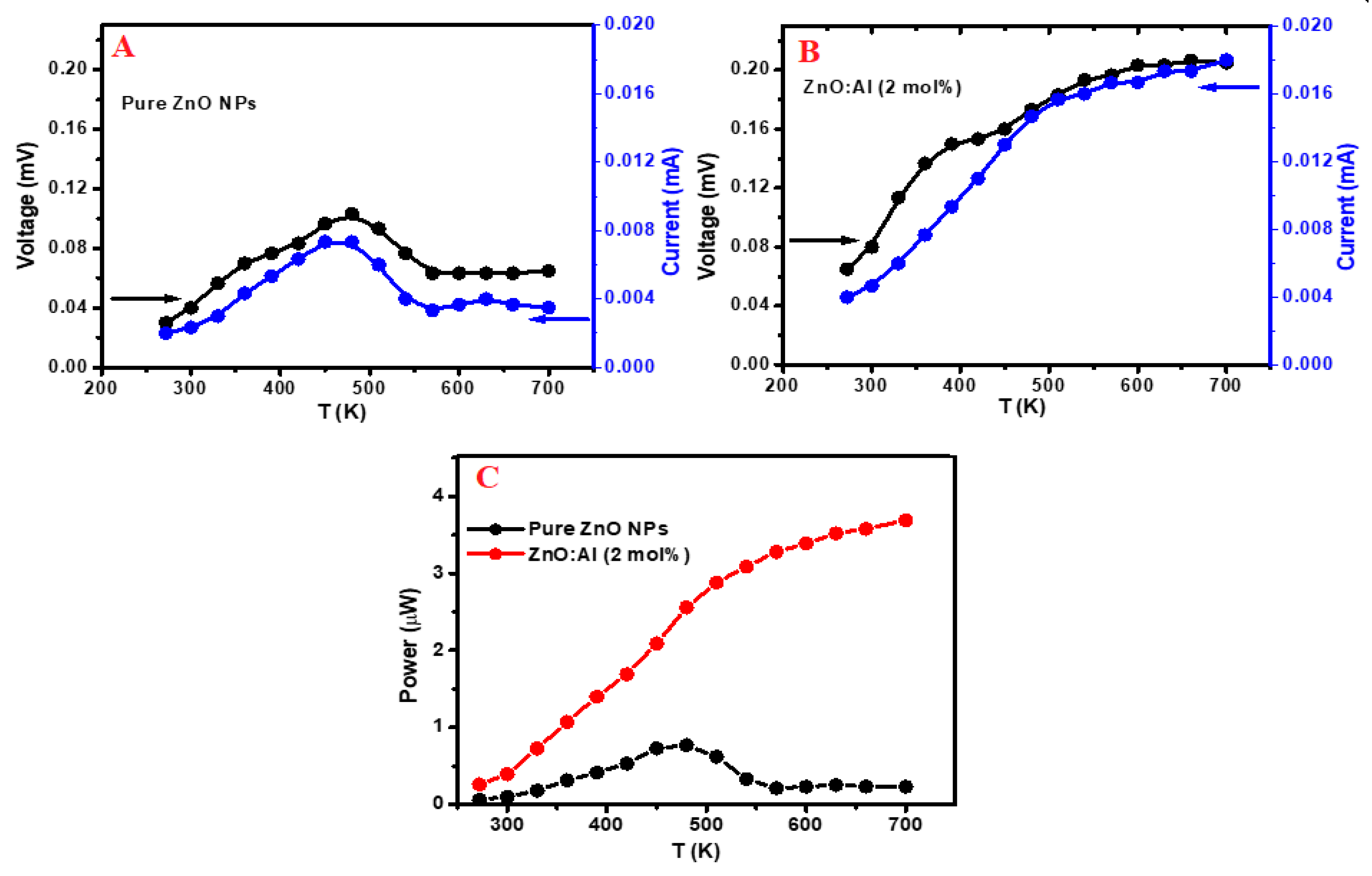
3.3. Power Measurements

The output voltage, current, and power of simple modules made of the pure and 2 mol % Al doped ZnO NSs samples were measured under a temperature gradient between the two sides of the nanostructure cubes (Figure 9). Comparing the results of pure and the 2 mol % Al-doped ZnO, the latter showed better voltage, current, and power outputs performance across all temperatures. The maximum voltage and current achieved by the pure ZnO was 0.11 mV and 0.008 mA respectively at 485 K; as the temperature continued to raise, the voltage and current declined (Figure 9A). In contrast, the voltage and current of the doped sample (Figure 9B) rose steadily from room temperature to 675 K; achieving maximum voltage and current of 0.21 mV and 0.017 mA, respectively. Figure 9C shows the differences in output power between pure and doped ZnO NSs. The maximum power output of pure ZnO was 0.7 µW at 485 K (at ΔT = 30 K), which was considerably less than the maximum power output of the 2 mol % Al-doped ZnO sample that recorded 3.7 µW at 685 K. These results indicate that the Al doped ZnO NSs are preferable in terms of thermoelectric generation. A number of factors contributed to the enhanced output power of Al-doped ZnO, include the previously described high power factor and figure of merit. As a TE generator, electronic devices require a large number of p–n pairs. The present Al doped ZnO NSs can be considered as the n-type pair and another appropriate p-type pair can form the desired TE generator that can raise the power output for practical applications.

4. Conclusions

In this work, the TE properties of Al-doped ZnO nanostructures synthesized by the microwave irradiation method were investigated. This method was employed due to its ability to provide single crystalline ZnO nanostructures and also to adjust the nanostructure morphology/sizes, which has been found to be effective for providing highly efficient TE materials. This technique is also found to be useful to perfectly incorporate the Al dopant within the ZnO lattice at a uniform distribution across ZnO nanostructure. High Seebeck coefficient, electrical conductivity, and low thermal conductivity were achieved by Al doping. The optimum TE performance reported in this study was achieved at 2 mol % Al doping. This concentration showed an enhanced TE performance (higher zT and power output) of approximately 10 times higher than that of the pure ZnO NSs. The Al doped sample demonstrated functionality as a TE generator electronic device module. The output power can be amplified by using a large number of n–p pairs considering the present Al doped ZnO NSs as the n-type.

Author Contributions

Visualization, A.A. and K.K.; Writing—original draft, N.B.; Writing—review and editing, N.B. and N.S. All authors have read and agreed to the published version of the manuscript.

Funding

This work was funded by King Abdulaziz University, Jeddah, under grant no. RG-38194-1.

Acknowledgments

This project was funded by the Deanship of Scientific Research (DSR) at King Abdulaziz University, Jeddah, under grant no. RG-38-194-1. The authors, therefore, acknowledge with thanks DSR for technical and financial support.

Conflicts of Interest

The authors declare no conflict of interest.

References

  1. Dresselhaus, M.S.; Chen, G.; Tang, M.Y.; Yang, R.G.; Lee, H.; Wang, D.Z.; Ren, Z.F.; Fleurial, J.-P.; Gogna, P. New directions for low-dimensional thermoelectric materials. Adv. Mater. 2007, 19, 1043–1053. [Google Scholar] [CrossRef]
  2. Backhaus-Ricoult, M.; Rustad, J.; Moore, L.; Smith, C.; Brown, J. Semiconducting large bandgap oxides as potential thermoelectric materials for high-temperature power generation? Appl. Phys. A 2014, 116, 433–470. [Google Scholar] [CrossRef]
  3. Hébert, S.; Berthebaud, D.; Daou, R.; Bréard, Y.; Pelloquin, D.; Guilmeau, E.; Gascoin, F.; Lebedev, O.; Maignan, A. Searching for new thermoelectric materials: Some examples among oxides, sulfides and selenides. J. Phys. Condens. Matter. 2015, 28, 013001. [Google Scholar] [CrossRef] [Green Version]
  4. Weintraub, B.; Zhou, Z.; Li, Y.; Deng, Y. Solution synthesis of one-dimensional ZnO nanomaterials and their applications. Nanoscale 2010, 2, 1573–1587. [Google Scholar] [CrossRef]
  5. Janotti, A.; Van de Walle, C.G. New insights into the role of native point defects in ZnO. J. Cryst. Growth 2006, 287, 58–65. [Google Scholar] [CrossRef]
  6. Jood, P.; Mehta, R.J.; Zhang, Y.; Peleckis, G.; Wang, X.; Siegel, R.W.; Borca-Tasciuc, T.; Dou, S.X.; Ramanath, G. Al-Doped Zinc Oxide nanocomposites with enhanced thermoelectric properties. Nano Lett. 2011, 11, 4337–4342. [Google Scholar] [CrossRef] [PubMed]
  7. Kang, K.-M.; Choi, Y.-J.; Yeom, G.Y.; Park, H.-H. Thickness-dependent growth orientation of F-doped ZnO films formed by atomic layer deposition. J. Vac. Sci. Technol. A 2016, 34, 01A144. [Google Scholar] [CrossRef] [Green Version]
  8. Liu, Y.; Lian, J. Optical and electrical properties of aluminum-doped ZnO thin films grown by pulsed laser deposition. Appl. Surf. Sci. 2007, 253, 3727–3730. [Google Scholar] [CrossRef]
  9. Mickan, M.; Helmersson, U.; Rinnert, H.; Ghanbaja, J.; Muller, D.; Horwat, D. Room temperature deposition of homogeneous, highly transparent and conductive Al-doped ZnO films by reactive high power impulse magnetron sputtering. Sol. Energy Mater. Sol. Cells 2016, 157, 742–749. [Google Scholar] [CrossRef] [Green Version]
  10. Vettumperumal, R.; Kalyanaraman, S.; Thangavel, R. Photoconductive UV detectors based heterostructures of Cd and Mg doped ZnO sol gel thin films. Mater. Chem. Phys. 2014, 145, 237–242. [Google Scholar] [CrossRef]
  11. Park, K.C.; Ma, D.Y.; Kim, K.H. The physical properties of Al-doped zinc oxide films prepared by RF magnetron sputtering. Thin Solid Films 1997, 305, 201–209. [Google Scholar] [CrossRef]
  12. Salah, N.; Al-Shawafi, W.M.; Alshahrie, A.; Baghdadi, N.; Soliman, Y.M.; Memic, A. Size controlled, antimicrobial ZnO nanostructures produced by the microwave assisted route. Mater. Sci. Eng. C 2019, 99, 1164–1173. [Google Scholar] [CrossRef] [PubMed]
  13. Wang, M.; Lee, K.E.; Hahn, S.H.; Kim, E.J.; Kim, S.; Chung, J.S.; Shin, E.W.; Park, C. Optical and photoluminescent properties of sol-gel Al-doped ZnO thin films. Mater. Lett. 2007, 61, 1118–1121. [Google Scholar] [CrossRef]
  14. Li, J.; Xu, J.; Xu, Q.; Fang, G. Preparation and characterization of Al doped ZnO thin films by sol–gel process. J. Alloys Compd. 2012, 542, 151–156. [Google Scholar] [CrossRef]
  15. Mote, V.D.; Purushotham, Y.; Dole, B.N. Williamson-Hall analysis in estimation of lattice strain in nanometer-sized ZnO particles. J. Theor. Appl. Phys. 2012, 6, 6. [Google Scholar] [CrossRef] [Green Version]
  16. Park, K.; Ko, K.Y. Effect of TiO2 on high-temperature thermoelectric properties of ZnO. J. Alloys Compd. 2007, 430, 200–204. [Google Scholar] [CrossRef]
  17. Ohtaki, M.; Tsubota, T.; Eguchi, K. Thermoelectric properties of oxide solid solutions based on Al-doped ZnO; Proceedings ICT98 (Cat. No.98TH8365). In Proceedings of the Seventeenth International Conference on Thermoelectrics, Piscataway, NJ, USA, 24–28 May 1998; pp. 610–613. [Google Scholar]
  18. Shirouzu, K.; Ohkusa, T.; Hotta, M.; Enomoto, N.; Hojo, J. Distribution and solubility limit of Al in Al2O3-doped ZnO sintered body. J. Ceram. Soc. Jpn. 2007, 115, 254–258. [Google Scholar] [CrossRef] [Green Version]
  19. Hong, M.-H.; Choi, H.; Shim, D.I.; Cho, H.H.; Kim, J.; Park, H.-H. Study of the effect of stress/strain of mesoporous Al-doped ZnO thin films on thermoelectric properties. Solid State Sci. 2018, 82, 84–91. [Google Scholar] [CrossRef]
  20. Mallika, A.; RamachandraReddy, A.; SowriBabu, K.; Reddy, K.V. Synthesis and optical characterization of aluminum doped ZnO nanoparticles. Ceram. Int. 2014, 40, 12171–12177. [Google Scholar] [CrossRef]
  21. Shao, C.-L.; Guan, H.-Y.; Wen, S.-B.; Chen, B.; Han, D.-X.; Gong, J.; Yang, X.-H.; Liu, Y.-C. Preparation and characterization of NiO nanofibers via an electrospinning technique. Chem. J. Chin. Univ. Chin. Ed. 2004, 25, 1015–1017. [Google Scholar]
  22. Yogamalar, N.R.; Bose, A.C. Absorption–emission study of hydrothermally grown Al: ZnO nanostructures. J. Alloys Compd. 2011, 509, 8493–8500. [Google Scholar] [CrossRef]
  23. Jule, L.; Dejene, F.; Ali, A.G.; Roro, K.; Mwakikunga, B. Defect-induced room temperature ferromagnetic properties of the Al-doped and undoped ZnO rod-like nanostructure. Mater. Lett. 2017, 199, 151–155. [Google Scholar] [CrossRef]
  24. Decremps, F.; Pellicer-Porres, J.; Saitta, A.M.; Chervin, J.-C.; Polian, A. High-pressure Raman spectroscopy study of wurtzite ZnO. Phys. Rev. B 2002, 65, 092101. [Google Scholar] [CrossRef] [Green Version]
  25. Chen, J.; Wang, J.; Zhuo, R.; Yan, D.; Feng, J.; Zhang, F.; Yan, P. The effect of Al doping on the morphology and optical property of ZnO nanostructures prepared by hydrothermal process. Appl. Surf. Sci. 2009, 255, 3959–3964. [Google Scholar] [CrossRef]
  26. Hong, W.S. Reaction Sintering of ZnO-Al2O3. Master’s Thesis, University of California, Berkeley, CA, USA, May 1991. [Google Scholar]
  27. Lindsay, J.R.; Rose, H.J.; Swartz, W.E.; Watts, P.H.; Rayburn, K.A. X-ray photoelectron spectra of aluminum oxides: Structural effects on the “chemical shift”. Appl. Spectrosc. 1973, 27, 1–5. [Google Scholar] [CrossRef]
  28. Nefedov, V.; Firsov, M.; Shaplygin, I. Electronic structures of MRhO2, MRh2O4, RhMO4 and Rh2MO6 on the basis of X-ray spectroscopy and ESCA data. J. Electron. Spectrosc. Relat. Phenom. 1982, 26, 65–78. [Google Scholar] [CrossRef]
  29. Bai, S.; Guo, T.; Zhao, Y.; Luo, R.; Li, D.; Chen, A.; Liu, C.C. Mechanism enhancing gas sensing and first-principle calculations of Al-doped ZnO nanostructures. J. Mater. Chem. A 2013, 1, 11335–11342. [Google Scholar] [CrossRef]
  30. Wang, J.; Li, Y.; Kong, Y.; Zhou, J.; Wu, J.; Wu, X.; Qin, W.; Jiao, Z.; Jiang, L. Non-fluorinated superhydrophobic and micro/nano hierarchical Al doped ZnO film: The effect of Al doping on morphological and hydrophobic properties. RSC Adv. 2015, 5, 81024–81029. [Google Scholar] [CrossRef]
  31. Uma, K.; Rusop, M.; Soga, T.; Jimbo, T. Effects of Al content on Zn0.95Mg0.05O thin films deposited by sol–gel spin coating. Jpn. J. Appl. Phys. 2007, 46, 40. [Google Scholar] [CrossRef]
  32. Kinemuchi, Y.; Ito, C.; Kaga, H.; Aoki, T.; Watari, K. Thermoelectricity of Al-doped ZnO at different carrier concentrations. J. Mater. Res. 2007, 22, 1942–1946. [Google Scholar] [CrossRef]
  33. Mondarte, E.A.; Copa, V.; Tuico, A.; Vergara, C.J.; Estacio, E.; Salvador, A.; Somintac, A. Al-doped ZnO and N-doped CuxO thermoelectric thin films for self-powering integrated devices. Mater. Sci. Semicond. Process. 2016, 45, 27–31. [Google Scholar] [CrossRef]
  34. Cheng, H.; Xu, X.; Hng, H.; Ma, J. Characterization of Al-doped ZnO thermoelectric materials prepared by RF plasma powder processing and hot press sintering. Ceram. Int. 2009, 35, 3067–3072. [Google Scholar] [CrossRef]
  35. Ohtaki, M.; Araki, K.; Yamamoto, K. High thermoelectric performance of dually doped ZnO ceramics. J. Electron. Mater. 2009, 38, 1234–1238. [Google Scholar] [CrossRef]
  36. Cai, K.; Müller, E.; Drašar, C.; Mrotzek, A. Preparation and thermoelectric properties of Al-doped ZnO ceramics. Mater. Sci. Eng. B 2003, 104, 45–48. [Google Scholar] [CrossRef]
  37. Zhou, H.M.; Yi, D.Q.; Yu, Z.M.; Xiao, L.R.; Li, J. Preparation of aluminum doped zinc oxide films and the study of their microstructure, electrical and optical properties. Thin Solid Films 2007, 515, 6909–6914. [Google Scholar] [CrossRef]
  38. Fujishiro, Y.; Miyata, M.; Awano, M.; Maeda, K. Effect of microstructural control on thermoelectric properties of hot-pressed Aluminum-Doped Zinc Oxide. J. Am. Ceram. Soc. 2003, 86, 2063–2066. [Google Scholar] [CrossRef]
  39. Katsuyama, S.; Takagi, Y.; Ito, M.; Majima, K.; Nagai, H.; Sakai, H.; Yoshimura, K.; Kosuge, K. Thermoelectric properties of (Zn1−yMgy)1−xAlxO ceramics prepared by the polymerized complex method. J. Appl. Phys. 2002, 92, 1391–1398. [Google Scholar] [CrossRef]
  40. Özgür, Ü.; Alivov, Y.I.; Liu, C.; Teke, A.; Reshchikov, M.; Doğan, S.; Avrutin, V.; Cho, S.-J.; Morkoç, H. A comprehensive review of ZnO materials and devices. J. Appl. Phys. 2005, 98, 11. [Google Scholar] [CrossRef] [Green Version]
  41. Tsubota, T.; Ohtaki, M.; Eguchi, K.; Arai, H. Thermoelectric properties of Al-doped ZnO as a promising oxidematerial for high-temperature thermoelectric conversion. J. Mater. Chem. 1997, 7, 85–90. [Google Scholar] [CrossRef]
  42. Sugahara, T.; Ohtaki, M.; Souma, T. Fabrication and power generation characteristics of p-NaCo2O4/n-ZnO oxide thermoelectric modules. In Proceedings of the 25th International Conference on Thermoelectrics, Vienna, Austria, 6–10 August 2006. [Google Scholar]
  43. Kulsi, C.; Dhara, P.; Mitra, M.; Kargupta, K.; Ganguly, S.; Banerjee, D. Effect of solvent on nanostructure and thermoelectric properties of bismuth. Indian J. Phys. 2016, 90, 557–562. [Google Scholar] [CrossRef]
  44. Ghosh, T.; Bardhan, M.; Bhattacharya, M.; Satpati, B. Study of inelastic mean free path of metal nanostructures using energy filtered transmission electron microscopy imaging. J. Microsc. 2015, 258, 253–258. [Google Scholar] [CrossRef] [PubMed]
Figure 1. X-ray diffraction of pure and Al doped ZnO NSs (A), magnified area of (1, 0, 0) plane (B).
Crystals 10 00610 g001
Figure 2. SEM images of (A) pure and Al doped ZnO NSs, (B) 0.5 mol %, (C) 1 mol %, (D) 2 mol %, and (E) 3 mol %.
Crystals 10 00610 g002aCrystals 10 00610 g002b
Figure 3. TEM images of pure (A,B) and Al doped ZnO (C,D) at a concentration of 3 mol %. The corresponding HRTEM d-spacing measurements are shown in (E,F).
Crystals 10 00610 g003aCrystals 10 00610 g003b
Figure 4. Elemental analysis of ZnO NSs doped with 3 mol % Al. (A) SEM mapping images of all the elements. Individual mapping of (B) Zn, (C) O, (D) Al. EDS quantitative and qualitative analysis is shown in (E).
Crystals 10 00610 g004
Figure 5. FTIR spectra of pure and Al doped ZnO NSs.
Crystals 10 00610 g005
Figure 6. Raman spectra of pure ZnO and Al-doped ZnO NSs.
Crystals 10 00610 g006
Figure 7. X-ray photoelectron spectroscopy of pure and 3 mol % Al doped ZnO NSs. (A) survey scan of the doped sample, the narrow scan of Zn2p3/2 in the doped sample (B), narrow scan of Al2p in the doped sample (C), and O1s in the doped sample (D). The peak positions of O1s in both pure and Al doped ZnO NSs is shown in (E).
Crystals 10 00610 g007aCrystals 10 00610 g007b
Figure 8. Thermo-electrical properties of pure and Al doped ZnO NSs. (A) Seebeck coefficient, (B) electrical conductivity, (C) power factor measurements, (D) thermal conductivity, and (E) figure of merit.
Crystals 10 00610 g008
Figure 9. Power measurement analysis of the pure and the 2 mol % Al doped ZnO NSs. Voltage–current curves of the pure ZnO NSs (A), and voltage–current curves of the 2 mol % Al doped ZnO NSs (B), output power measurements variation between the pure and 2 mol % Al doped ZnO NSs samples (C).
Crystals 10 00610 g009
Table 1. Lattice constant parameters and crystallite size of pure and Al doped ZnO NPs.
MaterialsLattice Constant Parameter (Å)Crystallite Size
abcc/a
Un-doped ZnO NPs3.2493.2495.2081.60318.7 nm
ZnO:Al NPs (0.5 mol %)3.2323.2325.1781.60223.5 nm
ZnO:Al NPs (1 mol %)3.2363.2365.1861.60227.6 nm
ZnO:Al NPs (2 mol %)3.2343.2345.1841.60324.1 nm
ZnO:Al NSs (3 mol %)3.2383.2385.1791.60017.6 nm
Table 2. EDX element percentage of each doped sample of Zn-Al 3%.
ElementWeight%Atomic%
C K11.9730.04
O K19.6236.96
Al K2.222.48
Zn66.1830.51
Table 3. Thermal conductivity measurements of pure ZnO NSs and Al doped ZnO.
MaterialsTemperature
(°C)
Thermal Conductivity
(W/m·K)
Specific Heat
(J/K·Kg)
Thermal Diffusivity
(m2·s−1)
Pure ZnO NSsR.T. *2.70.360.029
4004.30.940.013
ZnO Al 0.5% AlR.T. *2.80.340.021
4004.81.960.010
ZnO Al 1% AlR.T. *1.70.350.020
4003.51.280.011
ZnO Al 2% AlR.T. *0.970.340.012
4002.10.840.010
ZnO Al 3% AlR.T. *0.920.310.010
4001.220.570.006
* R.T. = room temperature.

