Material Properties of Zr–Cu–Ni–Al Thin Films as Diffusion Barrier Layer

Abstract
:1. Introduction
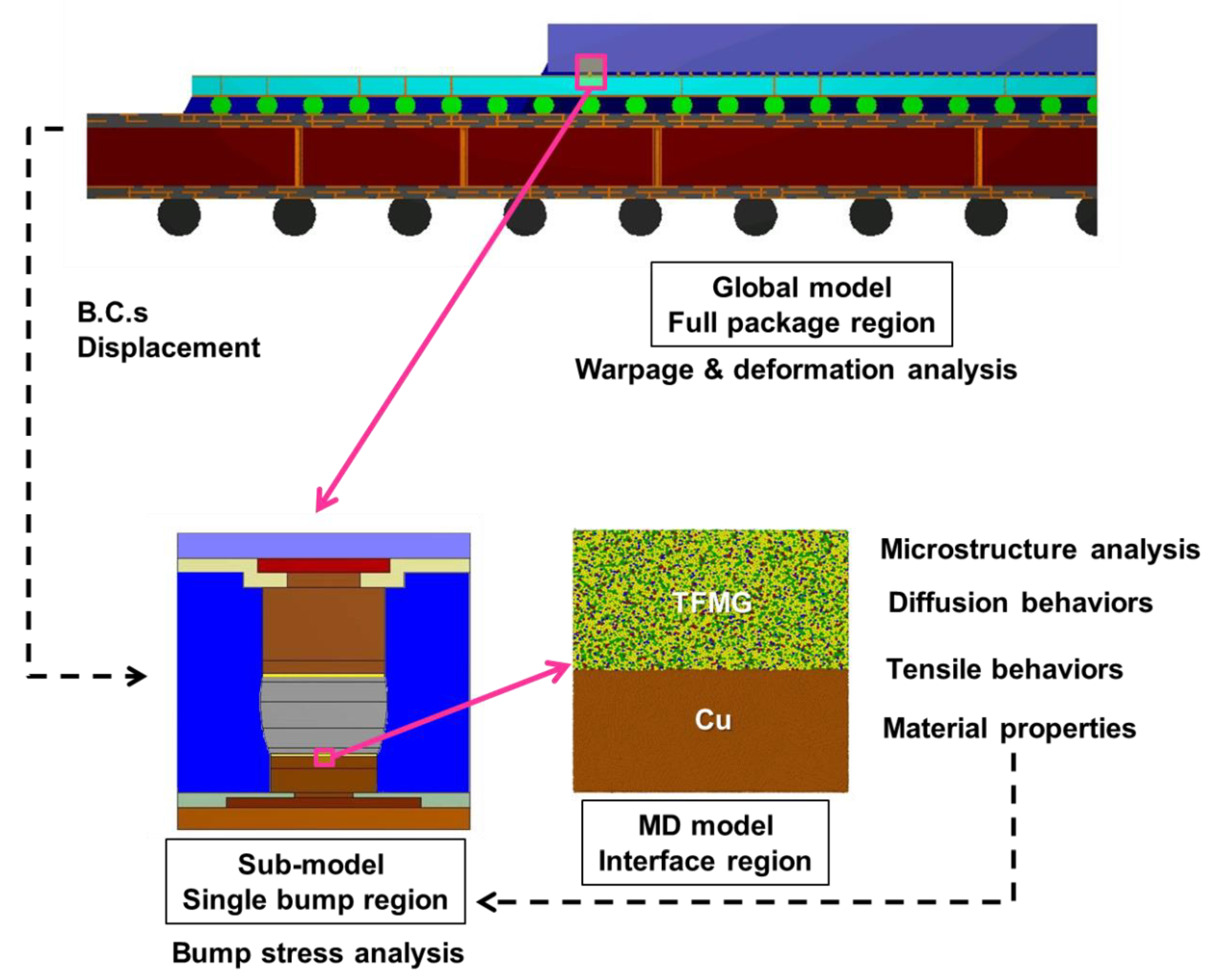
2. Methodology
2.1. Molecular Dynamics Simulation
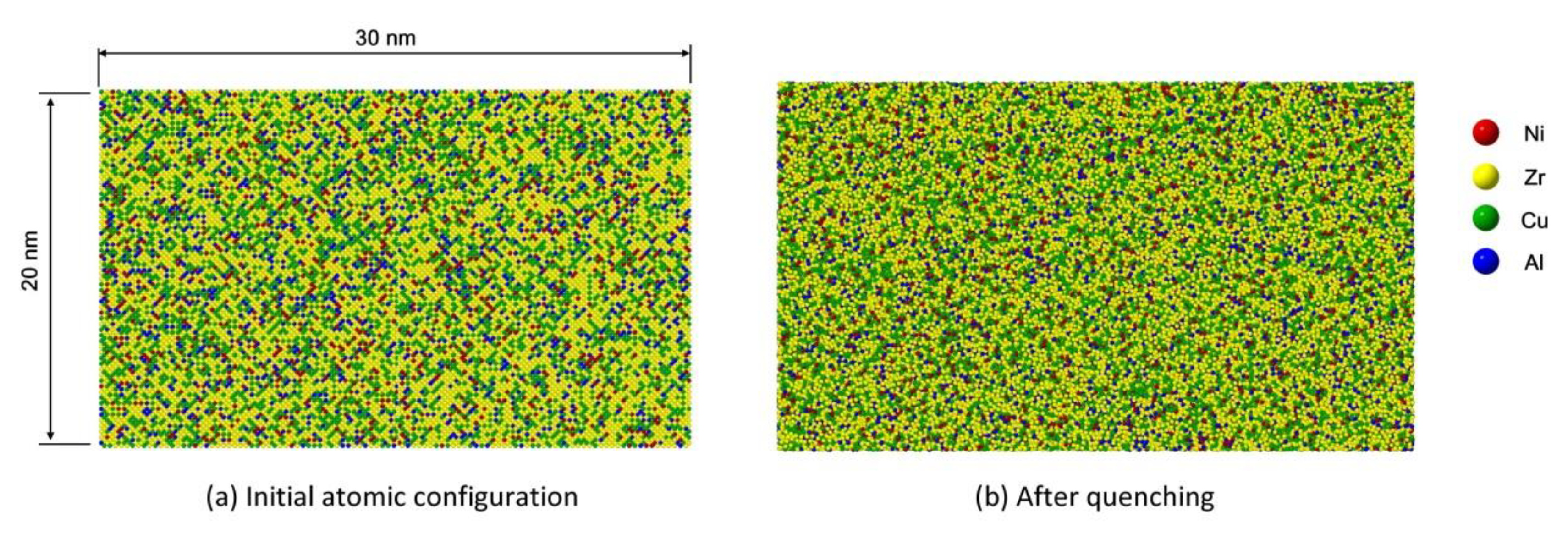
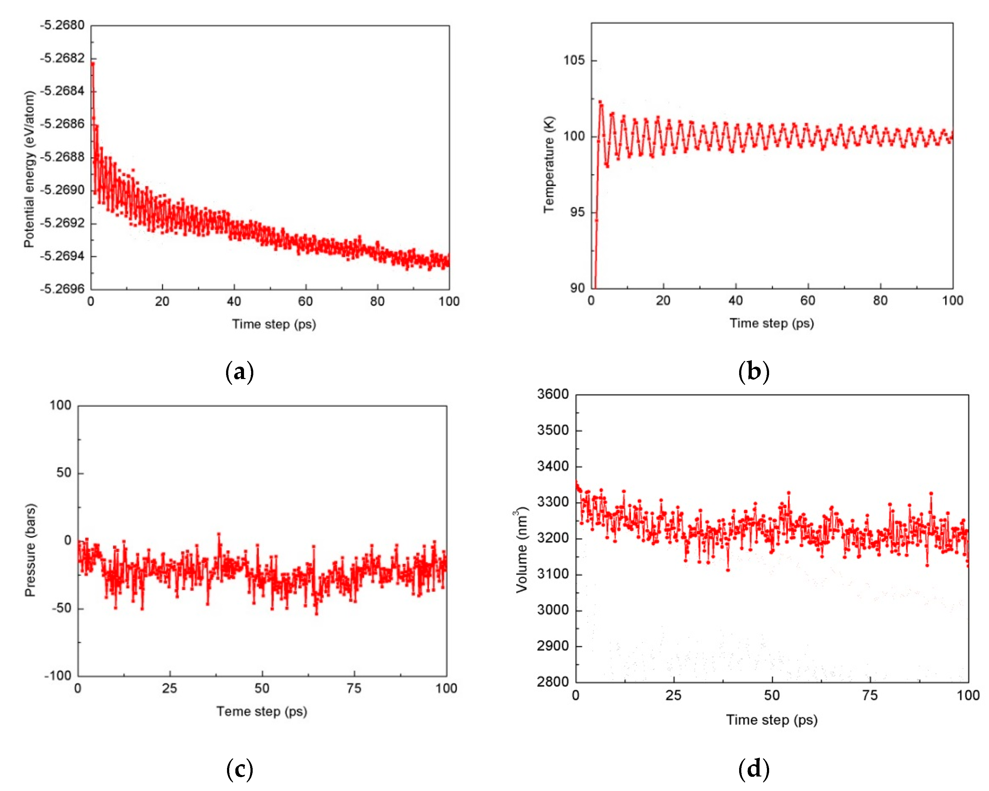
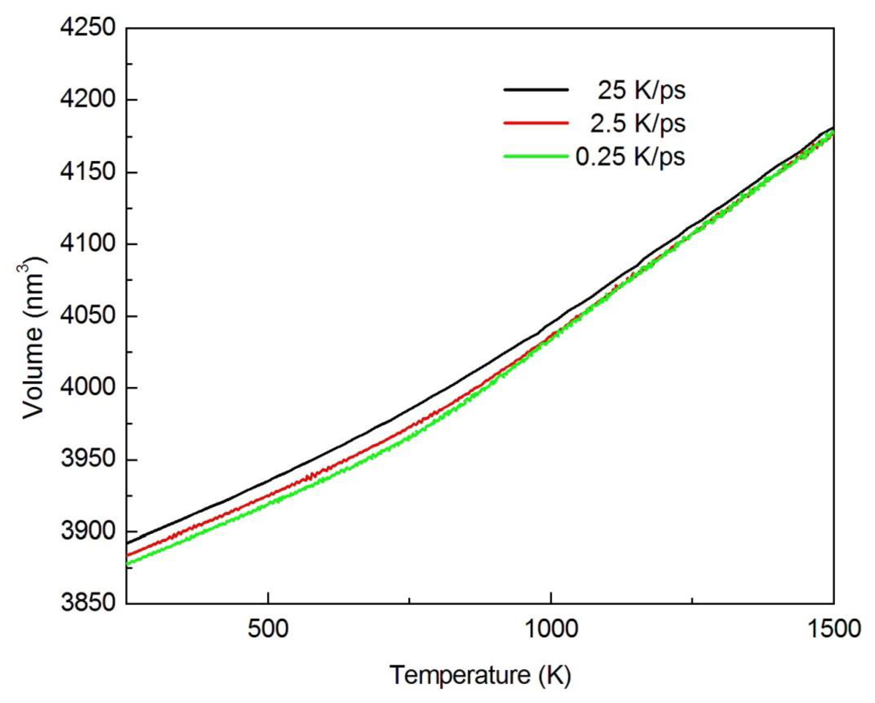
2.1.1. Amorphous Geometry Structure
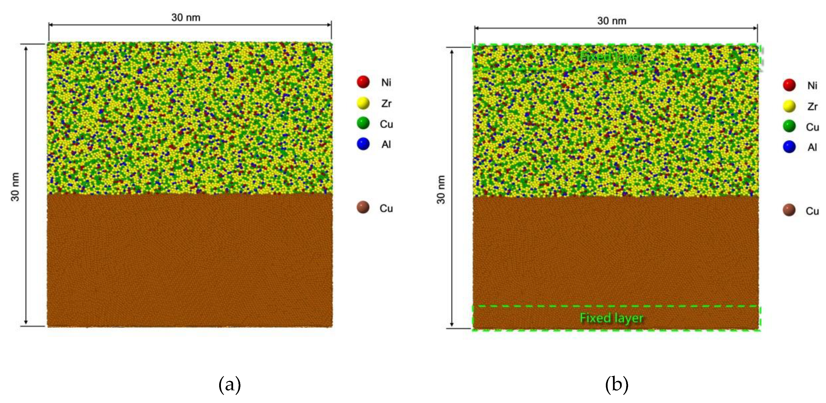
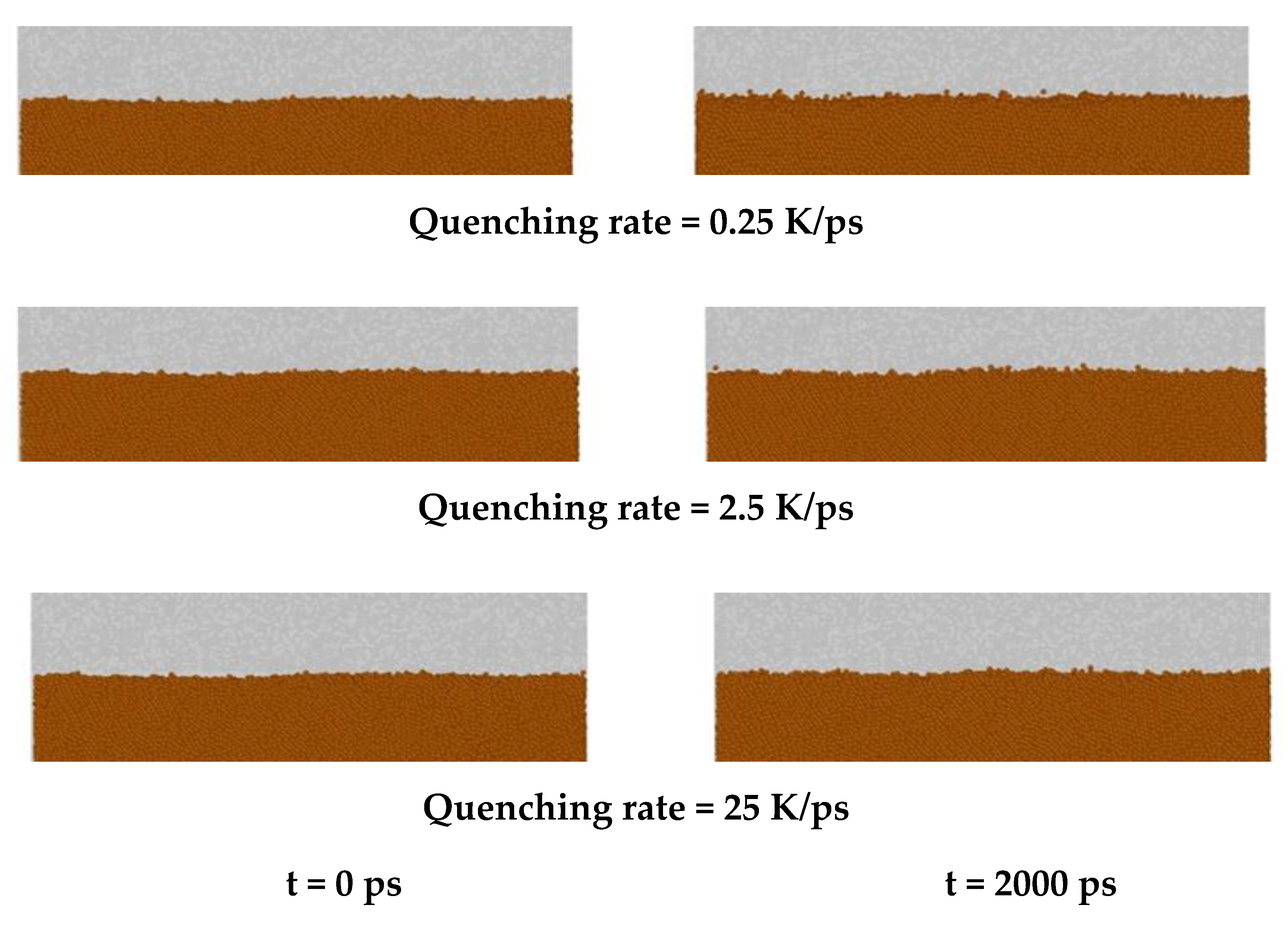
2.1.2. Procedure for Interface Model Preparation
2.1.3. Procedure for Diffusion and Deformation
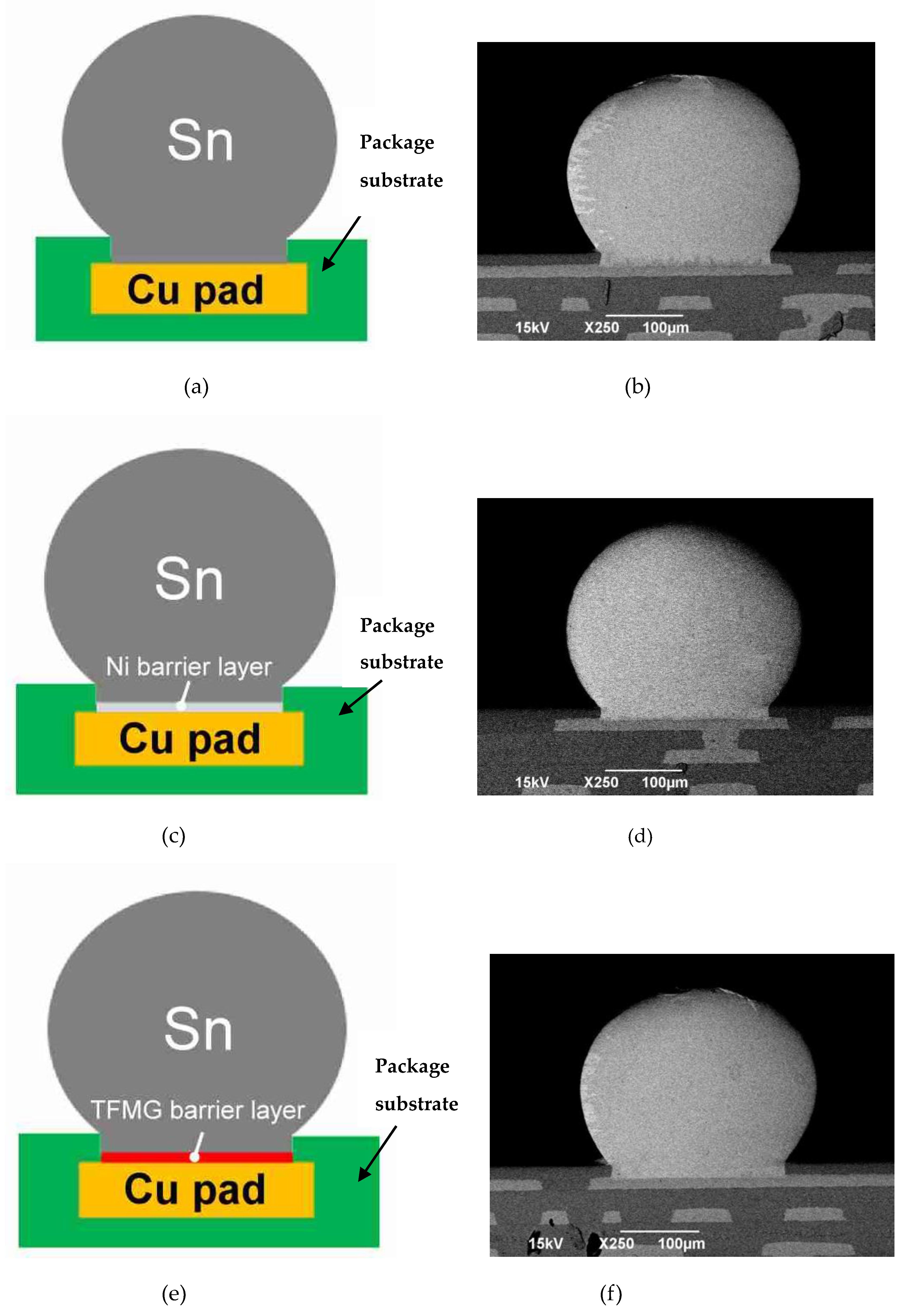
2.2. Sample Preparations and Experimental Verification
3. Results and Discussion
3.1. Simulation Results
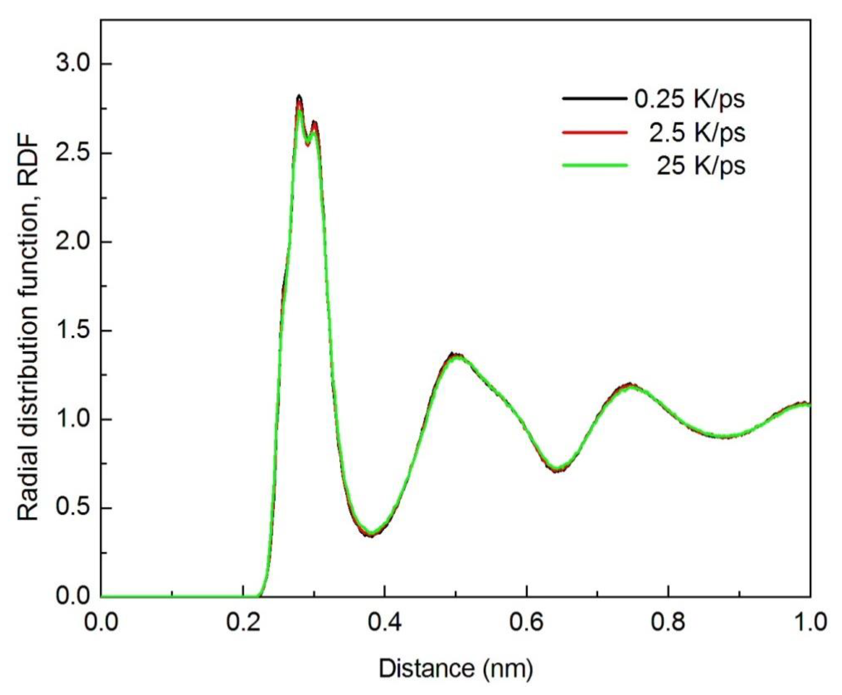
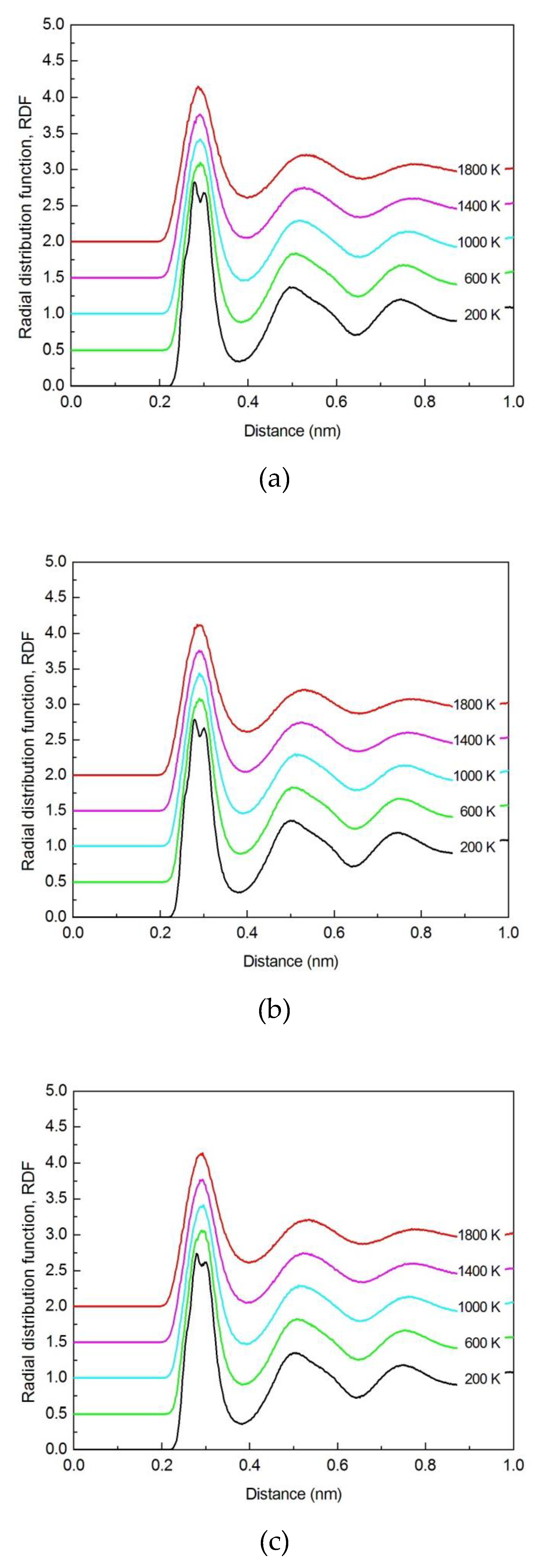
3.1.1. Radial Distribution Function (RDF)
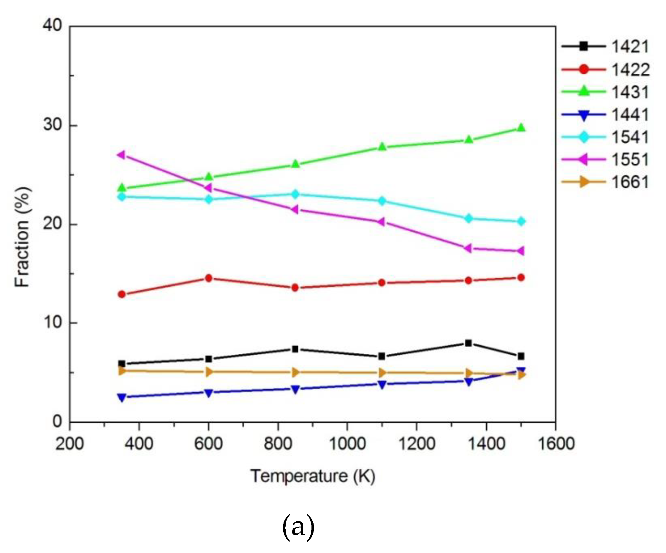
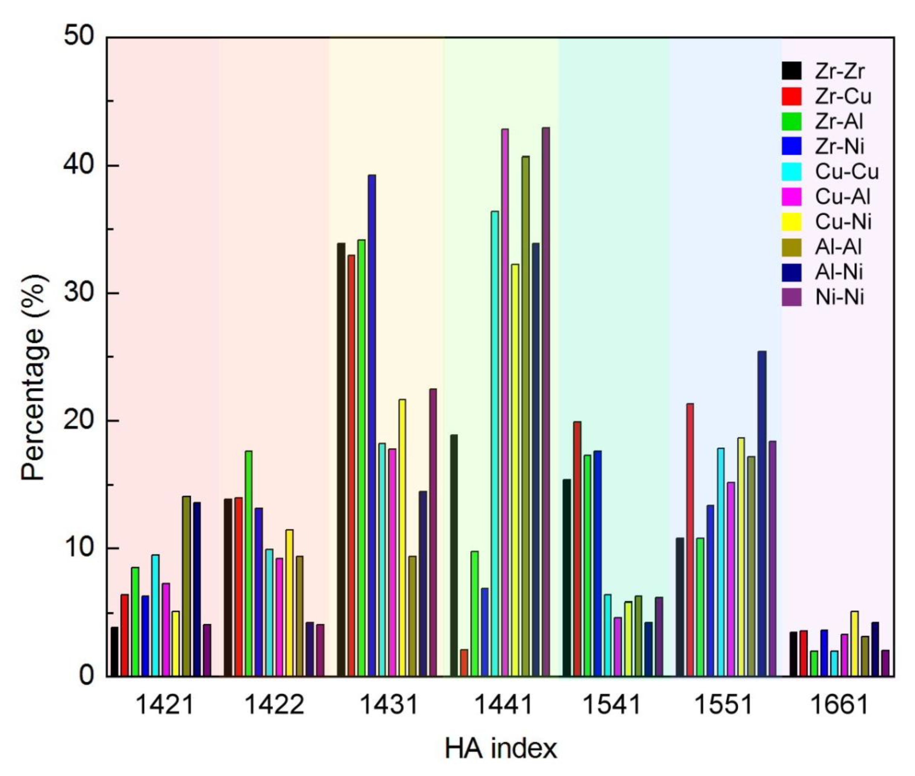
3.1.2. Honeycutt–Anderson (HA) Bond Pair Analysis
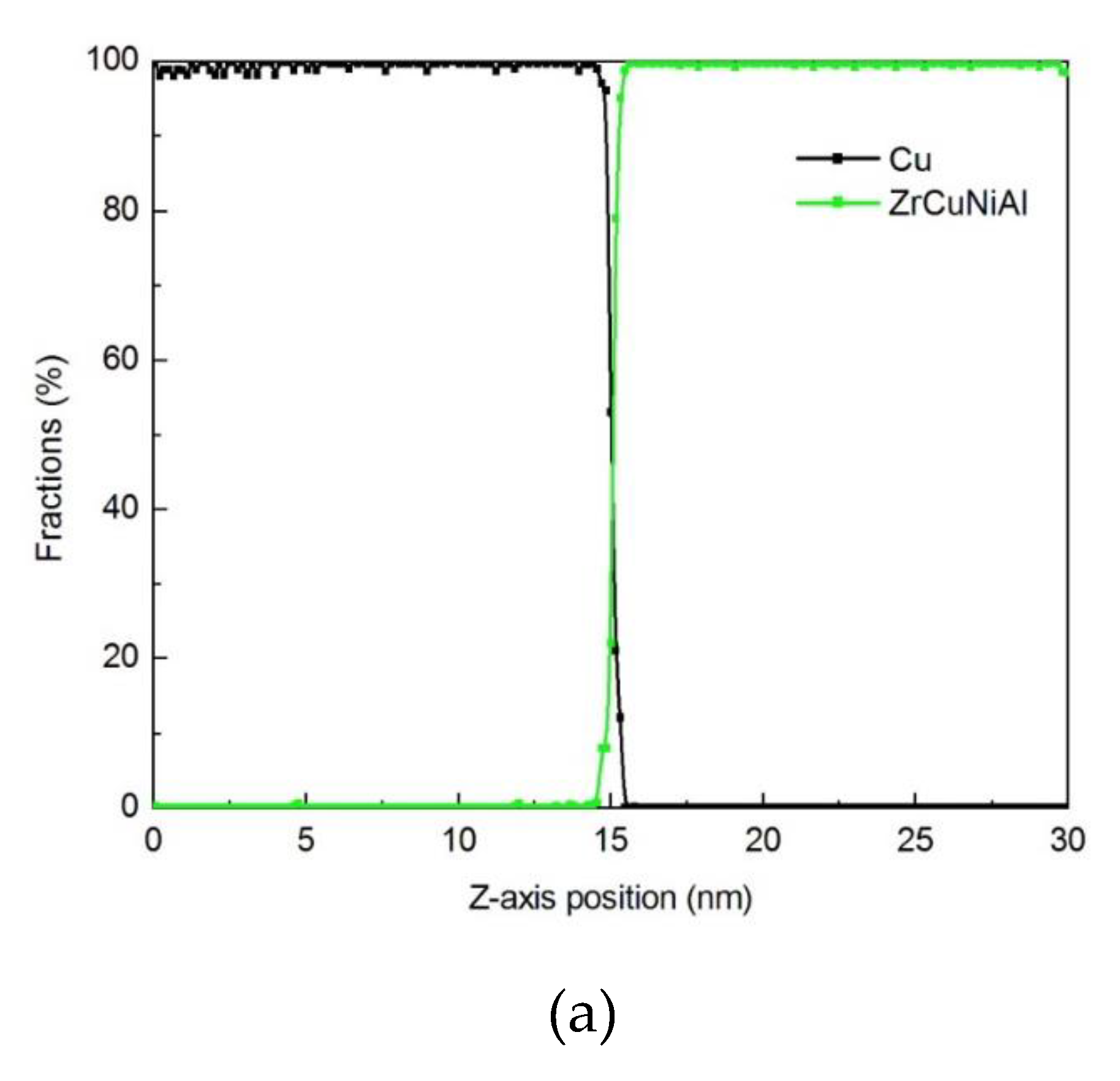
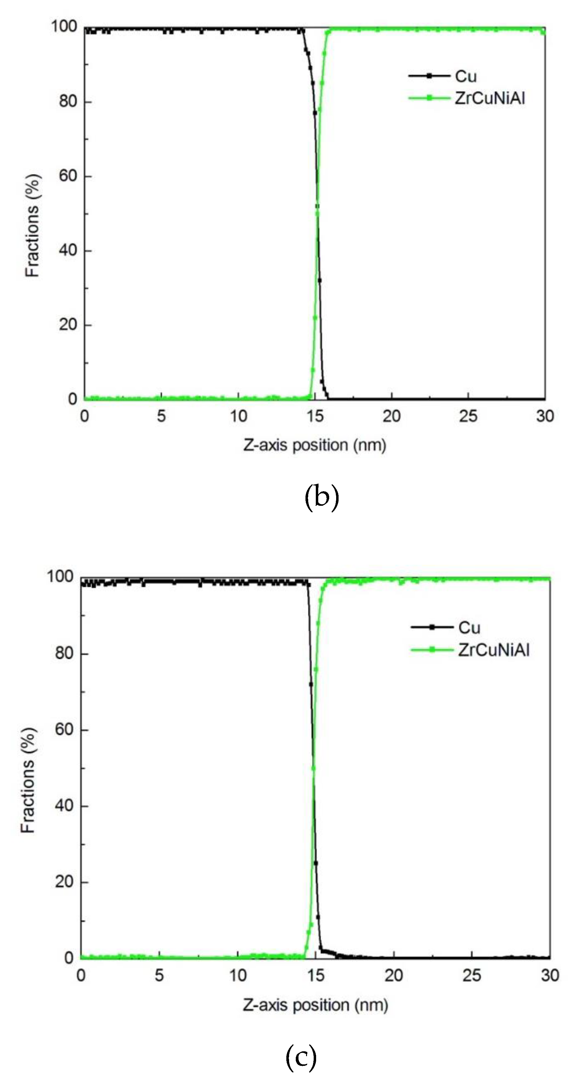
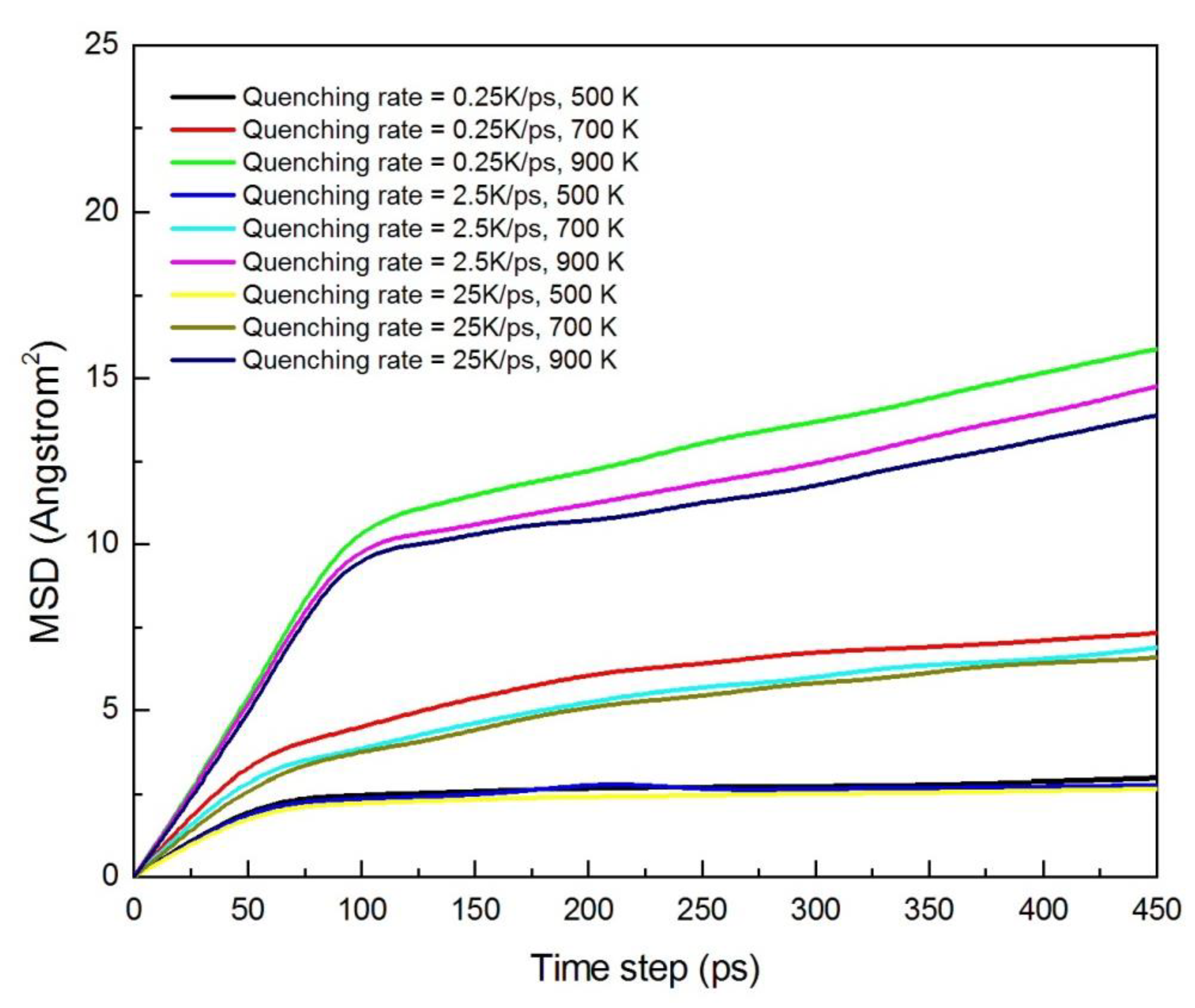
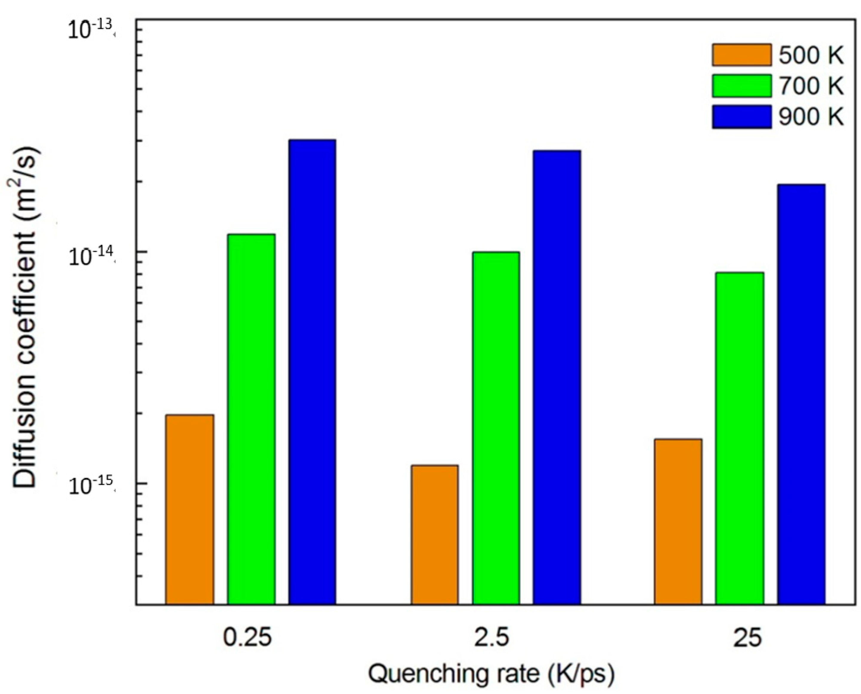
3.1.3. Diffusion Between Zr–Cu–Ni–Al and Cu
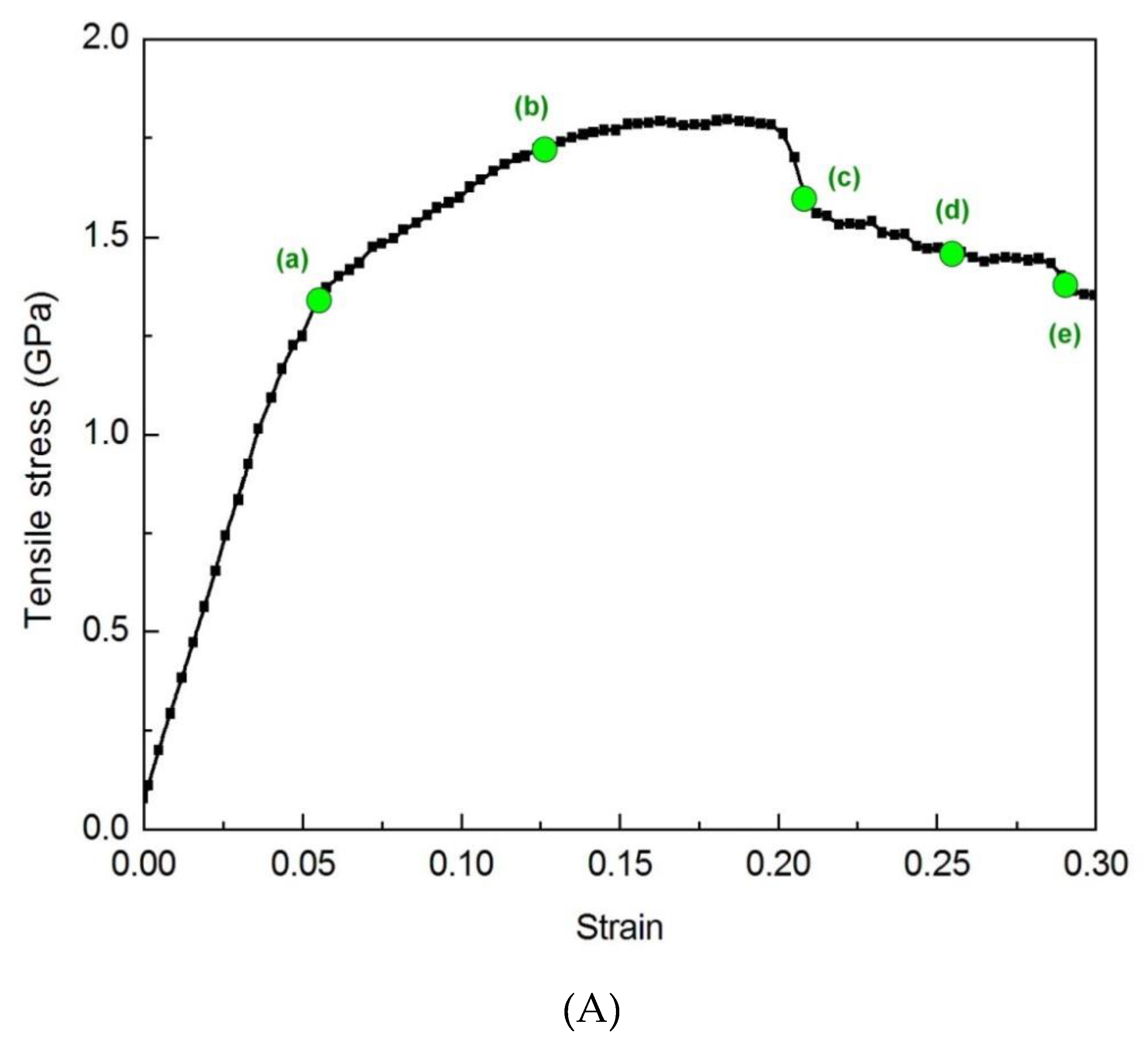
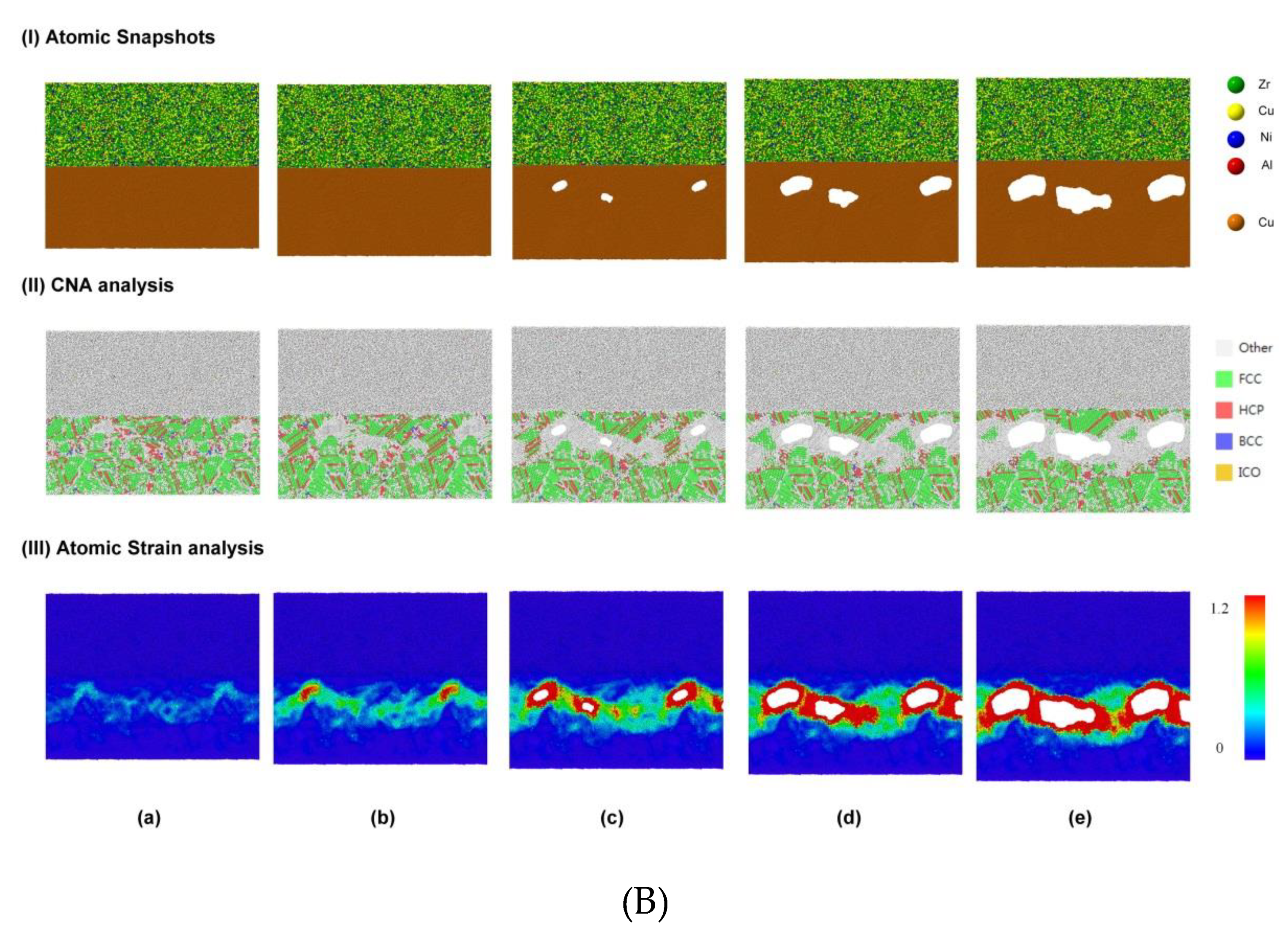
3.1.4. Tensile Behavior
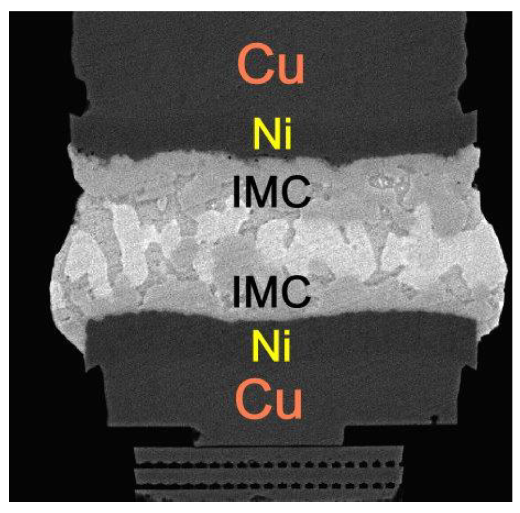
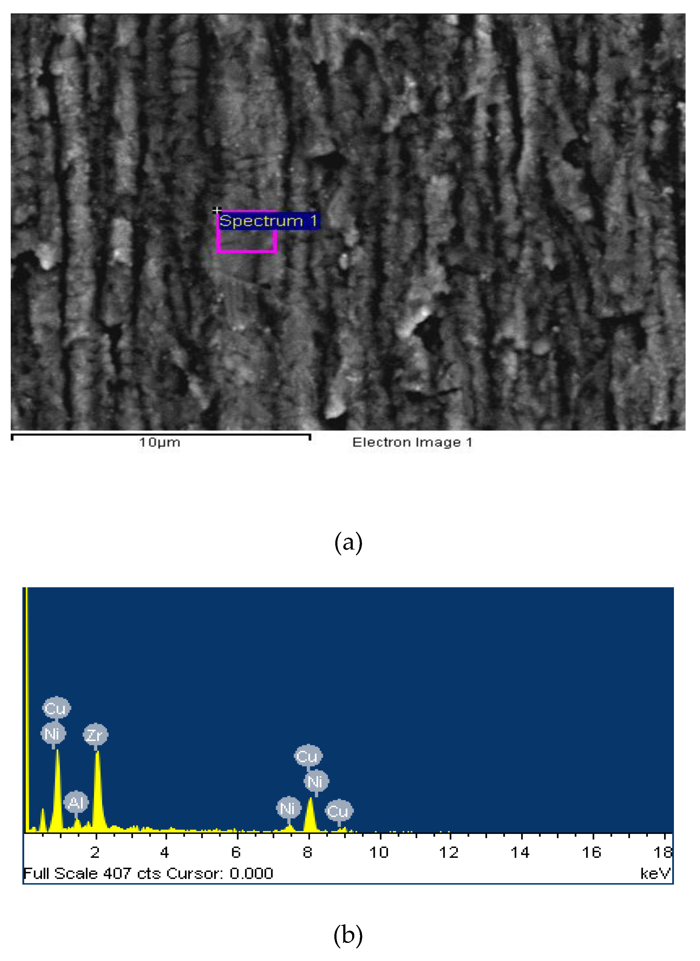
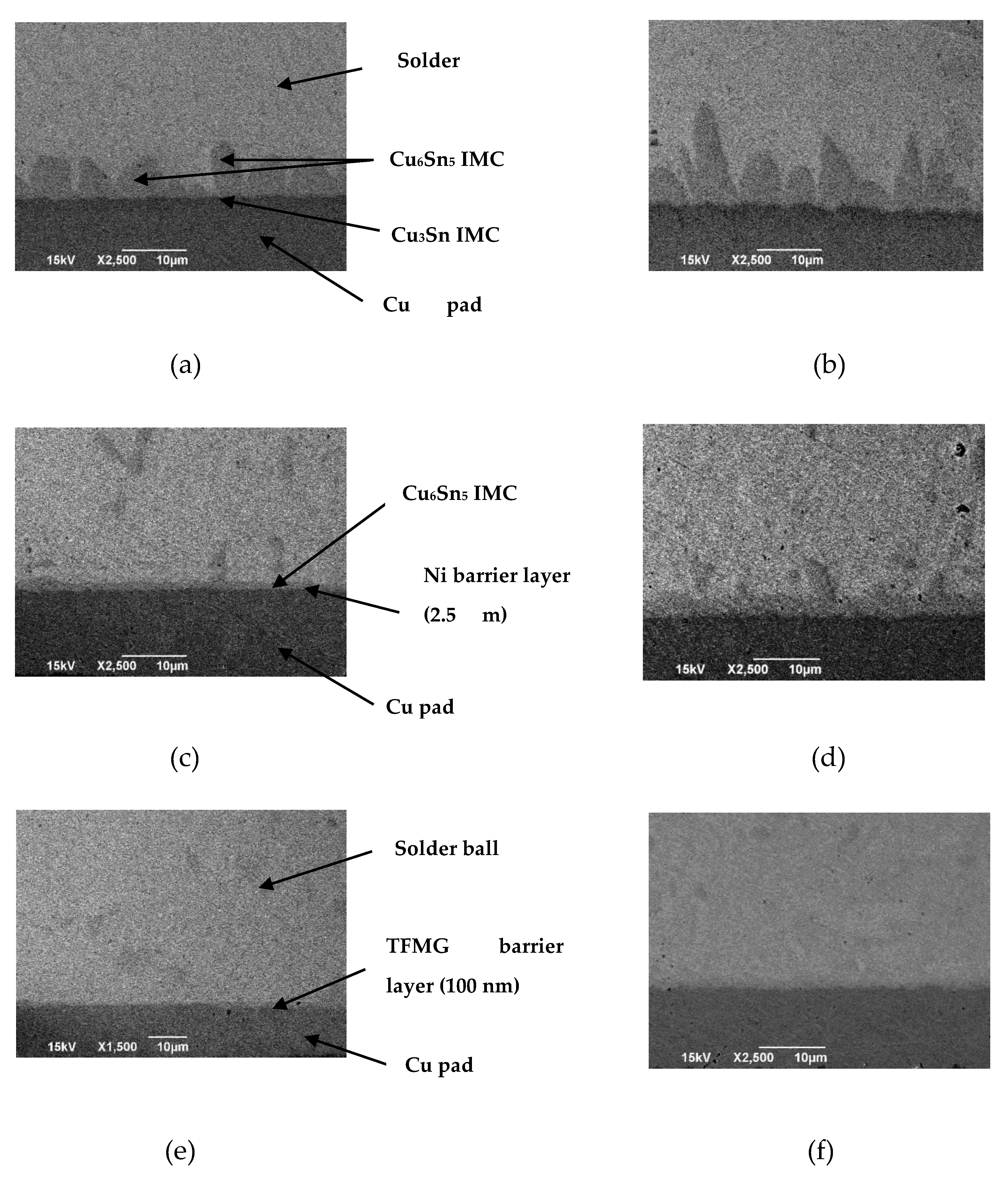
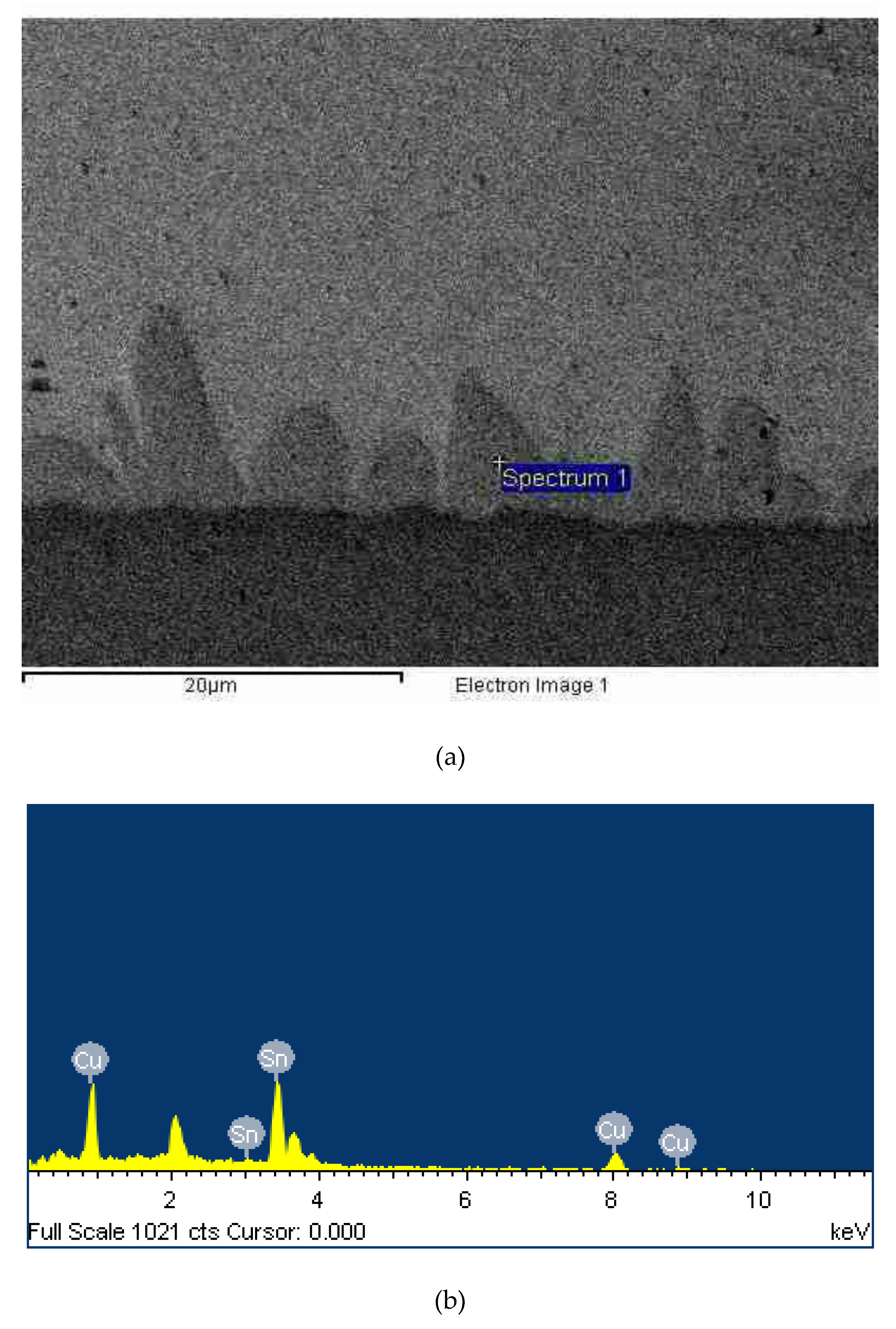
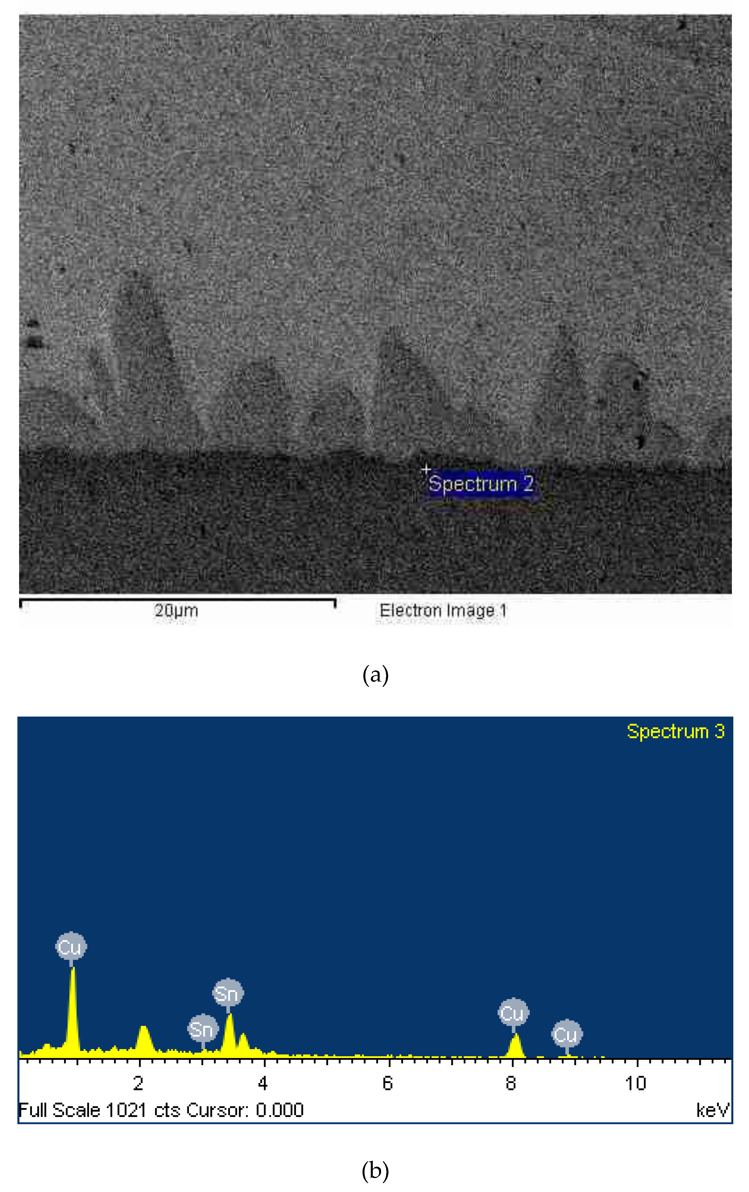
3.2. IMC Formation with Different Barrier Layers Via Experiment
4. Conclusions
Author Contributions
Funding
Conflicts of Interest
References
- Lim, S.P.S.; Ding, M.Z.; Kawano, M. Chip-to-Wafer (C2W) flip chip bonding for 2.5D high density interconnection on TSV free interposer. In Proceedings of the 2017 19th Electronics Packaging Technology Conference IEEE (EPTC, Singapore), Singapore, 6–9 December 2017; pp. 1–7. [Google Scholar]
- Murarka, S.P. Multilevel interconnections for ULSI and GSI era. Mater. Sci. Eng. R Rep. 1997, 19, 87–151. [Google Scholar] [CrossRef]
- Muehlbacher, M.; Bochkarev, A.S.; Mendez-Martin, F.; Sartory, B.; Chitu, L.; Popov, M.N.; Puschnig, P.; Spitaler, J.; Ding, H.; Schalk, N.; et al. Cu diffusion in single-crystal and polycrystalline TiN barrier layers: A high-resolution experimental study supported by first-principles calculations. J. Appl. Phys. 2015, 118, 085307. [Google Scholar] [CrossRef]
- Popov, M.N.; Bochkarev, A.S.; Razumovskiy, V.I.; Puschnig, P.; Spitaler, J. Point defects at the Σ5 (012)[100] grain boundary in TiN and the early stages of Cu diffusion: An ab initio study. Acta Mater. 2018, 144, 496–504. [Google Scholar] [CrossRef]
- Sangiovanni, D.G. Copper adatom, admolecule transport, and island nucleation on TiN (001) via ab initio molecular dynamics. Appl. Surf. Sci. 2018, 450, 180–189. [Google Scholar] [CrossRef]
- Wu, W.F.; Tsai, K.C.; Chao, C.G.; Chen, J.C.; Ou, K.L. Novel multilayered Ti/TiN diffusion barrier for Al metallization. J. Electr. Mater. 2005, 34, 1150–1156. [Google Scholar] [CrossRef]
- Lee, C.H.; Wong, Y.M.; Doherty, C.; Tai, K.L.; Lane, E.; Bacon, D.D.; Baiocchi, F.; Katz, A. Study of Ni as a barrier metal in AuSn soldering application for laser chip/submount assembly. J. Appl. Phys. 1992, 72, 3808–3815. [Google Scholar] [CrossRef]
- Chang, C.A. Interactions between Au and Cu across a Ni barrier layer. J. Appl. Phys. 1986, 50, 1220–1222. [Google Scholar] [CrossRef]
- Keller, H.N. Solder connections with a Ni barrier. IEEE Trans. Comp. Hybrids Manuf. Technol. 1986, 9, 433–439. [Google Scholar] [CrossRef]
- Iwamoto, N.; Truong, N.; Lee, E. New metal layers for integrated circuit manufacture: Experimental and modeling studies. Thin Solid Films 2004, 469, 431–437. [Google Scholar] [CrossRef]
- Chiang, K.N.; Lee, C.C.; Lee, C.C.; Chen, K.M. Current crowding-induced electromigration in Sn Ag 3.0 Cu 0.5 microbumps. Appl. Phys. Lett. 2006, 88, 072102. [Google Scholar] [CrossRef]
- Liu, Y.; Li, M.; Kim, D.W.; Gu, S.; Tu, K. Synergistic effect of electromigration and Joule heating on system level weak-link failure in 2.5 D integrated circuits. J. Appl. Phys. 2015, 118, 135304. [Google Scholar] [CrossRef]
- Li, M.; Tu, K.; Kim, D.W.; Gu, S. Electromigration induced thermomigration in microbumps by thermal cross-talk across neighboring chips in 2.5 D IC. In Proceedings of the 2016 IEEE International Reliability Physics Symposium (IRPS), Pasadena, CA, USA, 17–21 April 2016. [Google Scholar]
- Li, M.; Kim, D.W.; Gu, S.; Parkinson, D.Y.; Barnard, H.; Tu, K. Joule heating induced thermomigration failure in un-powered microbumps due to thermal crosstalk in 2.5 D IC technology. J. Appl. Phys. 2016, 120, 075105. [Google Scholar] [CrossRef]
- Jen, M.H.R.L.; Liu, C.; Lai, Y.S. Electromigration test on void formation and failure mechanism of FCBGA lead-free solder joints. IEEE Trans. Comp. Pack. Technol. 2009, 32, 79–88. [Google Scholar] [CrossRef]
- Rymaszewski, E.; Walsh, J.; Leehan, G. Semiconductor logic technology in IBM. IBM J. Res. Dev. 1981, 25, 603–616. [Google Scholar] [CrossRef]
- Zhang, Z.; Wong, C. Recent advances in flip-chip underfill: Materials, process, and reliability. IEEE Trans. Adv. Pack. 2004, 27, 515–524. [Google Scholar] [CrossRef]
- Ou, K.L.; Wu, W.F.; Chou, C.P.; Chiou, S.Y.; Wu, C.C. Improved TaN barrier layer against Cu diffusion by formation of an amorphous layer using plasma treatment. J. Vac. Sci. Technol. B 2002, 20, 2154–2161. [Google Scholar] [CrossRef]
- Wang, C.; Yiu, W.P.; Chu, J.P.; Shek, C.H.; Hsueh, C.H. Zr–Ti–Ni thin film metallic glass as a diffusion barrier between copper and silicon. J. Mater. Sci. 2015, 50, 2085–2092. [Google Scholar] [CrossRef]
- Diyatmika, W.; Chu, J.P.; Yen, Y.; Chang, W.; Hsueh, C. Thin film metallic glass as an underlayer for tin whisker mitigation: A room-temperature evaluation. Thin Solid Films. 2014, 561, 93–97. [Google Scholar] [CrossRef]
- Chao, B.; Chae, S.H.; Zhang, X.; Lu, K.H.; Im, J.; Ho, P.S. Investigation of diffusion and electromigration parameters for Cu–Sn intermetallic compounds in Pb-free solders using simulated annealing. Acta Mater. 2007, 55, 2805–2814. [Google Scholar] [CrossRef]
- Köster, U.; Meinhardt, J.; Roos, S.; Liebertz, H. Formation of quasicrystals in bulk glass forming Zr-Cu-Ni-Al alloy. Appl. Phys. Lett. 1996, 69, 179–181. [Google Scholar]
- Plimpton, S. Fast parallel algorithms for short-range molecular-dynamics. J. Comput. Phys. 1995, 117, 1–19. [Google Scholar] [CrossRef] [Green Version]
- Stukowski, A. Visualization and analysis of atomistic simulation data with OVITO-the Open Visualization Tool. Model. Simul. Mater. Sci. Eng. 2010, 18, 015012. [Google Scholar] [CrossRef]
- Rassoulinejad-Mousavi, S.M.; Mao, Y.; Zhang, Y. Evaluation of copper, aluminum, and nickel interatomic potentials on predicting the elastic properties. J. Appl. Phys. 2016, 119, 244304. [Google Scholar] [CrossRef]
- Daw, M.S.; Baskes, M.I. Embedded-atom method: Derivation and application to impurities, surfaces, and other defects in metals. Phys. Rev. B. 1984, 29, 6443. [Google Scholar] [CrossRef] [Green Version]
- Gupta, P.; Pal, S.; Yedla, N. Molecular dynamics based cohesive zone modeling of Al (metal)–Cu50Zr50 (metallic glass) interfacial mechanical behavior and investigation of dissipative mechanisms. Mater. Des. 2016, 105, 41–50. [Google Scholar] [CrossRef]
- Gear, C.W. Numerical Initial Value Problems in Ordinary Differential Equations; Prentice-Hall: Englewood Cliffs, NJ, USA, 1971. [Google Scholar]
- Barrett, C.; Massalski, T. Structure of Metals: Chap. 10; Brafman, O., Steinberger, I.T., Eds.; McGraw-Hill: New York, NY, USA, 1966. [Google Scholar]
- Tromans, D. Elastic anisotropy of HCP metal crystals and polycrystals. Inter. J. Res. Rev. Appl. Sci. 2011, 6, 462–483. [Google Scholar]
- Hearmon, R.F. The Elastic Constants of Crystals and Other Anisotropic Materials; Hellwege, K.-H., Hellwege, A.M., Landolt-Börnstein Tables, Group III, Eds.; Springer-Verlag: Berlin, Germany, 1979; Volume 11, pp. 1–154. [Google Scholar]
- Ledbetter, H.M.; Naimon, E.R. Elastic properties of metals and alloys. II. Copper. J. Phys. Chem. Ref. Data 1974, 3, 897–930. [Google Scholar] [CrossRef]
- Vallin, J.; Mongy, M.; Salama, K.; Beckman, O. Elastic constants of Aluminum. J. Appl. Phys. 1964, 35, 1825–1826. [Google Scholar] [CrossRef]
- Ledbetter, H.M.; Reed, R.P. Elastic properties of metals and alloys, I. Iron, Nickel, and Iron-Nickel Alloys. J. Phys. Chem. Ref. Data. 1973, 2, 531–617. [Google Scholar] [CrossRef] [Green Version]
- Edström, D.; Sangiovanni, D.G.; Hultman, L. Large-scale molecular dynamics simulations of TiN/TiN(001) epitaxial film growth. J. Vac. Sci. Technol. A. 2016, 34, 041509. [Google Scholar] [CrossRef] [Green Version]
- Edström, D.; Sangiovanni, D.G.; Hultman, L.; Petrov, I.; Greene, J.E.; Chirita, V. Effects of incident N atom kinetic energy on TiN/TiN(001) film growth dynamics: A molecular dynamics investigation. J. Appl. Phys. 2017, 121, 025302. [Google Scholar] [CrossRef] [Green Version]
- Chang, Y.; Hsu, K.; Li, J.; Tsai, P.; Jang, J.; Huang, J. Effect of cast process and microalloying on the fracture toughness of Zr-based bulk amorphous alloys. J. Alloys Comp. 2014, 614, 87–93. [Google Scholar] [CrossRef]
- Jang, S.C.; Jian, S.R.; Chang, C.F.; Chang, L.J.; Huang, Y.C.; Li, T.H.; Huang, J.C.; Liu, C.T. Thermal and mechanical properties of the Zr53Cu30Ni9Al8 based bulk metallic glass microalloyed with silicon. J. Alloys Comp. 2009, 478, 215–219. [Google Scholar] [CrossRef]
- Kato, H.; Chen, H.S.; Inoue, A. Relationship between thermal expansion coefficient and glass transition temperature in metallic glasses. Scr. Mater. 2008, 58, 1106–1109. [Google Scholar] [CrossRef]
- Fukami, T.; Yamamoto, H.; Sonobe, S.; Okai, D.; Yamasaki, T.; Zhang, T.; Inoue, A. Temperature dependence of linear expansion coefficient in metallic glass Zr-Al-Cu-Ni. J. Metastable Nanocrystalline Mater. 2005, 24, 487–490. [Google Scholar] [CrossRef]
- Honeycutt, J.; Andersen, H.C. Molecular-dynamics study of melting and freezing of small Lennard-Jones clusters. J. Phys. Chem. 1987, 91, 4950–4963. [Google Scholar] [CrossRef]
- Inoue, A. Stabilization of metallic supercooled liquid and bulk amorphous alloys. Acta Mater. 2000, 48, 279–306. [Google Scholar] [CrossRef]
- Chen, H.L.; Ju, S.P.; Wu, T.Y.; Liu, S.H.; Chen, H.T. Investigation of the mechanical properties and local structural evolution of Ti60Zr10Ta15Si15 bulk metallic glass during tensile deformation: A molecular dynamics study. RSC Adv. 2015, 5, 55383–55395. [Google Scholar] [CrossRef]
- Lin, J.A.; Lin, C.K.; Liu, C.M.; Huang, Y.S.; Chen, C.; Chu, D.T.; Tu, K.N. Formation mechanism of porous Cu3Sn intermetallic compounds by high current stressing at high temperatures in low-bump-height solder joints. Crystals 2016, 6, 12. [Google Scholar] [CrossRef] [Green Version]
- Diyatmika, W.; Chu, J.P.; Yen, Y.; Hsueh, C. Sn whisker mitigation by a thin metallic-glass underlayer in Cu-Sn. Appl. Phys. Lett. 2013, 103, 241912. [Google Scholar] [CrossRef]
- Mookam, N.; Tunthawiroon, P.; Kanlayasiri, K. Effects of copper content in Sn-based solder on the intermetallic phase formation and growth during soldering. IOP Conf. Ser. Mater. Sci. Eng. 2018, 361, 012008. [Google Scholar] [CrossRef]
- Wu, Y.; Sees, J.A.; Pouraghabagher, C.; Foster, L.A.; Marshall, J.L.; Jacobs, E.G.; Pinizzotto, R.F. The formation and growth of intermetallics in composite solder. J. Electr. Mater. 1993, 22, 769–777. [Google Scholar] [CrossRef]


| Element | Methods | C11 (GPa) | C12 (GPa) | C44 (GPa) |
|---|---|---|---|---|
| Cu | Experimental data [25] | 168.4 | 121.4 | 75.4 |
| Calculated data by MD | 168.5 | 120.8 | 75.2 | |
| Error | 0.06% | 0.49% | 0.27% | |
| Zr | Experimental data [29] | 144 | 74 | 33.4 |
| Calculated data by MD | 141 | 74.2 | 44 | |
| Error | 2.1% | 2.7% | 31.7% | |
| Ni | Experimental data [25] | 253 | 152 | 124 |
| Calculated data by MD | 240.4 | 144.1 | 122.7 | |
| Error | 4.98% | 5.20% | 1.05% | |
| Al | Experimental data [25] | 107.3 | 60.1 | 28.3 |
| Calculated data by MD | 102.6 | 58.8 | 27.7 | |
| Error | 4.38% | 2.16% | 2.12% |
| Element | Weight% | Atomic% |
|---|---|---|
| Al | 2.40 | 6.62 |
| Ni | 8.14 | 10.04 |
| Cu | 31.44 | 32.50 |
| Zr | 58.02 | 50.84 |
| Totals | 100.00 |
| Element | Weight% | Atomic% |
|---|---|---|
| Cu | 40.51 | 55.99 |
| Sn | 59.49 | 44.01 |
| Totals | 100.00 |
| Element | Weight% | Atomic% |
|---|---|---|
| Cu | 62.56 | 75.74 |
| Sn | 37.44 | 24.26 |
| Totals | 100.00 |
© 2020 by the authors. Licensee MDPI, Basel, Switzerland. This article is an open access article distributed under the terms and conditions of the Creative Commons Attribution (CC BY) license (http://creativecommons.org/licenses/by/4.0/).
Share and Cite
Sung, P.-H.; Chen, T.-C. Material Properties of Zr–Cu–Ni–Al Thin Films as Diffusion Barrier Layer. Crystals 2020, 10, 540. https://doi.org/10.3390/cryst10060540
Sung P-H, Chen T-C. Material Properties of Zr–Cu–Ni–Al Thin Films as Diffusion Barrier Layer. Crystals. 2020; 10(6):540. https://doi.org/10.3390/cryst10060540
Chicago/Turabian StyleSung, Po-Hsien, and Tei-Chen Chen. 2020. "Material Properties of Zr–Cu–Ni–Al Thin Films as Diffusion Barrier Layer" Crystals 10, no. 6: 540. https://doi.org/10.3390/cryst10060540