Spectroscopic and Microscopic Correlation of SRO-HFCVD Films on Quartz and Silicon

 , , ,
, , ,  , , and
Abstract
:1. Introduction
2. Material and Methods
3. Results
4. Discussion
5. Conclusions
Author Contributions
Funding
Acknowledgments
Conflicts of Interest
References
- DiMaria, D.J.; Dong, D.W.; Theis, T.N.; Kirtley, J.R.; Tsang, J.C.; Young, D.R.; Pesavento, F.L. Charge transport and trapping phenomena in off-stoichiometric silicon dioxide films. J. Appl. Phys. 1983, 54, 5801–5827. [Google Scholar] [CrossRef]
- Canham, L.T. Silicon quantum wire array fabrication by electrochemical and chemical dissolution of wafers. Appl. Phys. Lett. 1990, 57, 1046. [Google Scholar] [CrossRef]
- Morales-Sánchez, A.; Leyva, K.M.; Aceves, M.; Barreto, J.; Domínguez, C.; Luna-López, J.A.; Carrillo, J.; Pedraza, J. Photoluminescence enhancement through silicon implantation on SRO-LPCVD films. Mater. Sci. Eng. B 2010, 174, 119–122. [Google Scholar] [CrossRef]
- Lin, Z.; Guo, Y.; Song, J.; Zhang, Y.; Song, C.; Wang, X.; Huang, R. Effect of thermal annealing on the blue luminescence of amorphous silicon oxycarbide films. J. Non-Cryst. Solids 2015, 428, 184–188. [Google Scholar] [CrossRef] [Green Version]
- Cabañas-Tay, S.A.; Palacios-Huerta, L.; Aceves-Mijares, M.; Coyopol, A.; Morales-Morales, F.; Pérez-García, S.A.; Licea-Jiménez, L.; Domínguez-Hornad, C.; Monfil-Leyva, K.; Morales-Sánchez, A. Study of narrow and intense UV electroluminescence from ITO/SRO/Si-p and ITO/SRN/SRO/Si-p based light-emitting capacitors. J. Lumin. 2017, 183, 334–340. [Google Scholar] [CrossRef]
- Pandey, R.K.; Patil, L.S.; Bange, J.P.; Patil, D.R.; Mahajan, A.M.; Patil, D.S.; Gautam, D.K. Growth and characterization of SiON thin films by using the thermal-CVD machine. Opt. Mater. 2004, 25, 1–7. [Google Scholar] [CrossRef]
- Hsieh, C.-R.; Chen, Y.-Y.; Lou, J.-C. Effect of fluorinated silicate glass passivation layer on electrical characteristics and dielectric reliabilities for the HfO2/SiON gate stacked nMOSFET. Microelectron. Eng. 2010, 87, 2241–2246. [Google Scholar] [CrossRef]
- Luna López, J.; Carrillo López, J.; Aceves Mijares, M.; Morales Sánchez, A.; Falcony, C. FTIR and photoluminescence of annealed silicon-rich oxide films. Superficies Vacío 2009, 22, 11–14. [Google Scholar]
- González Fernández, A.A. MOS-like electroluminescent devices using silicon-rich oxide obtained by LPCVD. In Proceedings of the 2009 6th International Conference on Electrical Engineering, Computing Science and Automatic Control (CCE), Toluca, Mexico, 10–13 January 2009. [Google Scholar]
- Benítez-Lara, A.; García-Salgado, G.; Vázquez-Valerdi, D.E.; Morales-Sánchez, A.; Espinosa-Torres, N.D.; Luna-López, J.A. Silicon rich oxide powders by HWCVD: Its optical and morphological properties. Adv. Powder Technol. 2015, 26, 163–168. [Google Scholar] [CrossRef]
- Valerdi, D.E.V.; López, J.A.L.; Salgado, G.G. Twofold SiOx Films deposited by HFCVD: It is Optical, Compositional and Electrical Properties. Procedia Eng. 2014, 87, 168–171. [Google Scholar] [CrossRef] [Green Version]
- Hernández Simon, Z.J. Propiedades Fotovoltaicas de Películas SRO depositadas mediante HFCVD en Estructuras ITO/SRO/Si y AU/SRO/Si. Master’s Thesis, Benemérita Universidad Autónoma de Puebla (BUAP), Puebla, Mexico, 2018. [Google Scholar]
- Mendoza Conde, G.O. Propiedades fotoeléctricas de películas de SRO depositadas mediante HFCVD en estructuras Au/SRO/Si. Master’s Thesis, Benemérita Universidad Autónoma de Puebla (BUAP), Puebla, Mexico, 2018. [Google Scholar]
- Chávez Velázquez, R.; Zaldivar Huerta, I.; Reyes Betanzo, C.; Díaz Sánchez, A. Fabricación de guías de onda ópticas en silicio utilizando óxido de silicio y nitruro de silicio. Superf. Vacío 2005, 18, 21–23. [Google Scholar]
- Luna-López, J.A.; García-Salgado, G.; Díaz-Becerril, T.; López, J.C.; Vázquez-Valerdi, D.E.; Juárez-Santiesteban, H.; Rosendo-Andrés, E.; Coyopol, A. FTIR, AFM and PL properties of thin SiOx films deposited by HFCVD. Mater. Sci. Eng. B 2010, 174, 88–92. [Google Scholar] [CrossRef]
- Philipp, H.R. Optical and bonding model for non-crystalline SiOx and SiOxNy Materials. J. Non Cryst. Solids 1972, 8–10, 627–632. [Google Scholar] [CrossRef]
- Chen, X.Y.; Lu, Y.F.; Tang, L.J.; Wu, Y. H Annealing and oxidation of silicon oxide films prepared by plasma-enhanced chemical vapor deposition. J. Appl. Phys. 2005, 97, 1–10. [Google Scholar] [CrossRef] [Green Version]
- Quiroga-González, E. On the photoluminescence of multilayer arrays of silicon-rich oxide with high silicon content prepared by low-pressure chemical vapor deposition. Thin Solid Film. 2011, 519, 8030–8036. [Google Scholar] [CrossRef]
- Sitarz, M. The structure of simple silicate glasses in the light of Middle Infrared spectroscopy studies. J. Non Cryst. Solids 2011, 357, 1603–1608. [Google Scholar] [CrossRef]
- Tomozeiu, N. Silicon Oxide (SiOx, 0<x<2): A Challenging Material for Optoelectronics. In Optoelectronics-Materials and Techniques; IntechOpen: London, UK, 2011; Chapter 3; pp. 55–98. [Google Scholar]
- Morales-Sánchez, A. Optical characterization of silicon-rich oxide films. Sens. Actuatorsa Phys. 2008, 142, 12–18. [Google Scholar] [CrossRef]
- Flores Gracia, F. Photoluminescence and cathodoluminescence characteristics of SiO2 and SRO films implanted with Si. Superficies y vacío. In Sociedad Mexicana de Ciencia y Tecnología de Superficies y Materiales A.C.; Distrito Federal: Mexico City, Mexico, 2005; Volume 18, pp. 7–13. [Google Scholar]
- Koshida, N. Device Applications of Silicon Nanocrystals and Nanostructures; Springer Science & Business Media: Berlin/Heidelberg, Germany, 2008. [Google Scholar]
- Zacharias, M.; Heitmann, J.; Scholz, R.; Kahler, U.; Schmidt, M.; Bläsing, J. Size-controlled highly luminescent silicon nanocrystals: A SiO/SiO 2 superlattice approach. Appl. Phys. Lett. 2002, 80, 661. [Google Scholar] [CrossRef]
- Álvarez, M.P.; Carreras, J.; Barreto, J.; Morales, A.; Domínguez, C.; Garrido, B. Efficiency and reliability enhancement of silicon nanocrystal field-effect luminescence from nitride-oxide gate stacks. Appl. Phys. Lett. 2009, 92, 241-104. [Google Scholar]
- Berencén, Y.; Ramírez, J.M.; Jambois, O.; Domínguez, C.; Rodríguez, J.A.; Garrido, B.J. Rare Earth-Doped Silicon-Based Light Emitting Devices: Towards new Integrated Photonic Building Blocks. Appl. Phys. 2012, 112, 022–114. [Google Scholar]
- Adams, A.C. Plasma Deposition of Inorganic Films. Solid State Technol. 1983, 26, 135–139. [Google Scholar]
- Tauc, J. Optical Properties and Electronic Structure of Amorphous Germanium. Phys. Status Solidi 1966, 15, 627. [Google Scholar] [CrossRef]
- Keinonen, J.; Djurabekova, F.; Nordlund, K. Silicon Nanophotonics Basic Principles, Present Status and Perspectives; Pan Stanford Publishing: New York, NY, USA, 2009; pp. 379–394. [Google Scholar]
- Sattler, K. Encyclopedia of Nanoscience and Nanotechnology: Silicon Nanowires; American Scientific Publishers: Valencia, CA, USA, 2004; Volume 9, pp. 815–835. [Google Scholar]
- Kwon, Y.H.; Park, C.J.; Lee, W.C. Memory effects to deep levels in metal-oxide-semiconductor structure with nanocrystalline Si. Appl. Phys. Lett. 2002, 80, 2502–2504. [Google Scholar] [CrossRef]
- Wang, Y.; Townsend, P.D. Common mistakes in luminescence analysis. J. Physics. Conf. Ser. 2012, 398, 012003. [Google Scholar] [CrossRef] [Green Version]
- Jaeger, R.C. Introduction to Microelectronic Fabrication; Addison-Wesley Publishing: Boston, MA, USA, 1990. [Google Scholar]
- Hung-Yu, T.; Chiao-Ti, L.; Lin-Hsuan, T.; Yung-Hsian, L.; Yi-Hao, P.; Chih-I, W.; Gong-Ru, L. SiC and Si Quantum Dots Co-Precipitated Si-Rich SiC Film with n- and p-Type Dopants Grown by Hydrogen-Free PECVD. ECS J. Solid State Sci. Technol. 2013, 2, N159–N164. [Google Scholar]


| Film | dff mm | dfs mm | Td mins | as Grown | Heat-Treated | ||||||
|---|---|---|---|---|---|---|---|---|---|---|---|
| Sample | Th nm | ηSRO | Silicon Excess % | Sample | Th nm | ηSRO | Silicon Excess % | ||||
| 25 | 6 | 8 | 3 | Si/SRO25 | 322.9 | 2.46 ± 0.03 | 9.9 | Si/SRO25 | 296.3 | 1.3 ± 0.04 | 5.5 |
| Q/SRO25 | 334.7 | Q/SRO25 | 311.2 | ||||||||
| 100 | Si/SRO100 | 319.6 | 2.039 ± 0.35 | 10.6 | Si/SRO100 | 283.5 | 1.02 ± 0.08 | 5.0 | |||
| Q/SRO100 | 314.7 | Q/SRO100 | 293.1 | ||||||||
| 5 | Si/SRO25/100 | 592.3 | 1.46 ± 0.06 | Si/SRO25/100 | 583.3 | 1.93 ± 0.31 | |||||
| Q/SRO25/100 | 647.5 | Q/SRO25/100 | 591.6 | ||||||||
| Si/SRO100/25 | 578.9 | 1.51 ± 0.02 | Si/SRO100/25 | 560.5 | 2.05 ± 0.65 | ||||||
| Q/SRO100/25 | 639.8 | Q/SRO100/25 | 594.0 | ||||||||
| SRO | Film Location | Oxidation Phases Peak Position (eV) | ||||
|---|---|---|---|---|---|---|
| Si0 | Si1+ | Si2+ | Si3+ | Si4+ | ||
| 25as-G | Surface | 99.7 | 102.8 | |||
| 25HT | 101.5 | 103.2, 103.8 | ||||
| 100as-G | 99.3 | 102.1, 102.7 | 103.7 | |||
| 100HT | 103.2, 104.1 | |||||
| 25as-G | Volume | 101.4 | 103.1 | |||
| 25HT | 101.2 | 103.2, 103.4 | ||||
| 100as-G | 100.7 | 103, 103.8 | ||||
| 100HT | 102 102.8 | 103.4 | ||||
| 25as-G | SRO/Si Interface | 100.2 | 102 | 103.3 | ||
| 25HT | 102.8 | 103.4 | ||||
| 100as-G | 99.4 | 102.5 | 103.4 | |||
| 100HT | 103.1, 103.4 | |||||
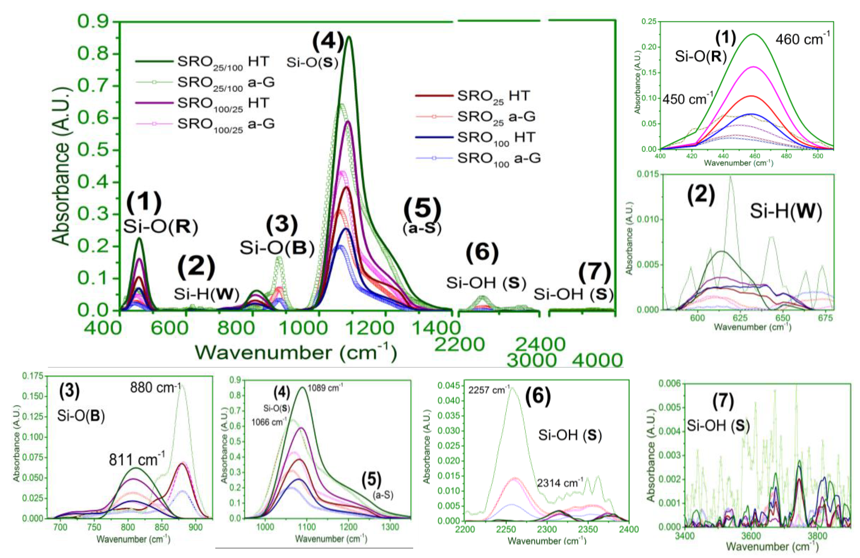
| Vibrational Modes | As Grown | SiO2 | Heat-Treated | ||||||
|---|---|---|---|---|---|---|---|---|---|
| S25 | S100 | S100/25 | S25/100 | S25 | S100 | S100/25 | S25/100 | ||
| Wave Number cm−1 | |||||||||
| (1) Si-O-Si in SiO2 Rolling (R) [13,14,15,16,20,21,22] | 450 | 449 | 448 | 449 | 458 | 459 | 457 | 458 | 459 |
| (2) Si-H Waggling (W) [17,23] | 610 | 612 | 612 | 619 | 616 | 620 | 625 | 614 | |
| (3) Si-O-Si in SiO2 Bending (B) [13,14,15,16,20,21,22] | 801 | 799 | 802 | 797 | 812 | 812 | 812 | 811 | 811 |
| (3) Si-OH Bending (B) [13,14,15,16,20,21,22] | 880 | 881 | 880 | 880 | 879 | 806 | 808 | 810 | |
| (4) Si-O-Si in SiO2 Stretching in-phase (S) [13,14,15,16,20,21,22] | 1066 | 1064 | 1062 | 1068 | 1082 | 1084 | 1082 | 1080 | 1088 |
| (5) Si-O-Si Stretching out of phase (a-S) [13,14,15,16,20,21,22] | 1163 | 1154 | 1168 | 1175 | 1177 | 1208 | 1192 | 1227 | 1230 |
| (6) Si-OH Stretching (S) [17,18] | 2258 | 2259 | 2258 | 2258 | 2315 | 2316 | 2315 | 2314 | |
| (7) Si-OH Stretching (S) [17,18,23] | 3669 | 3670 | 3743 | 3667 | 3744 | 3742 | 3813 | 3742 | |
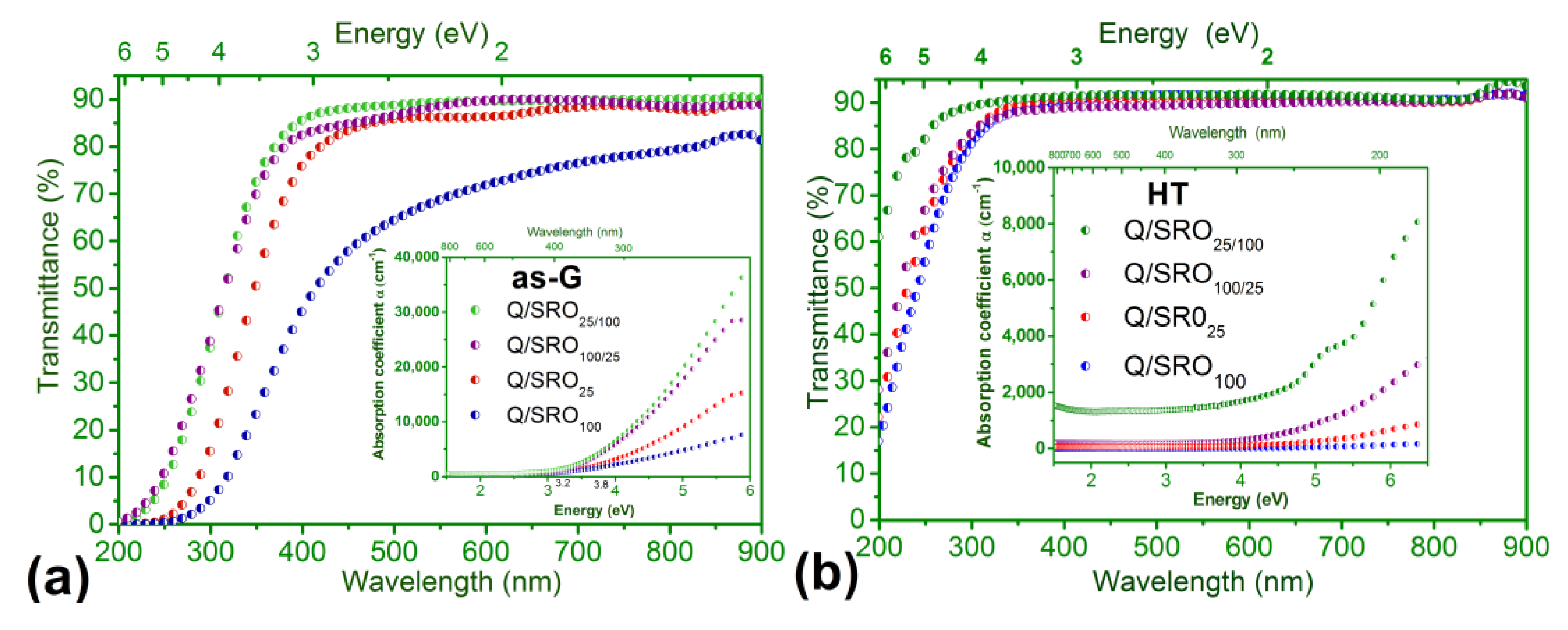
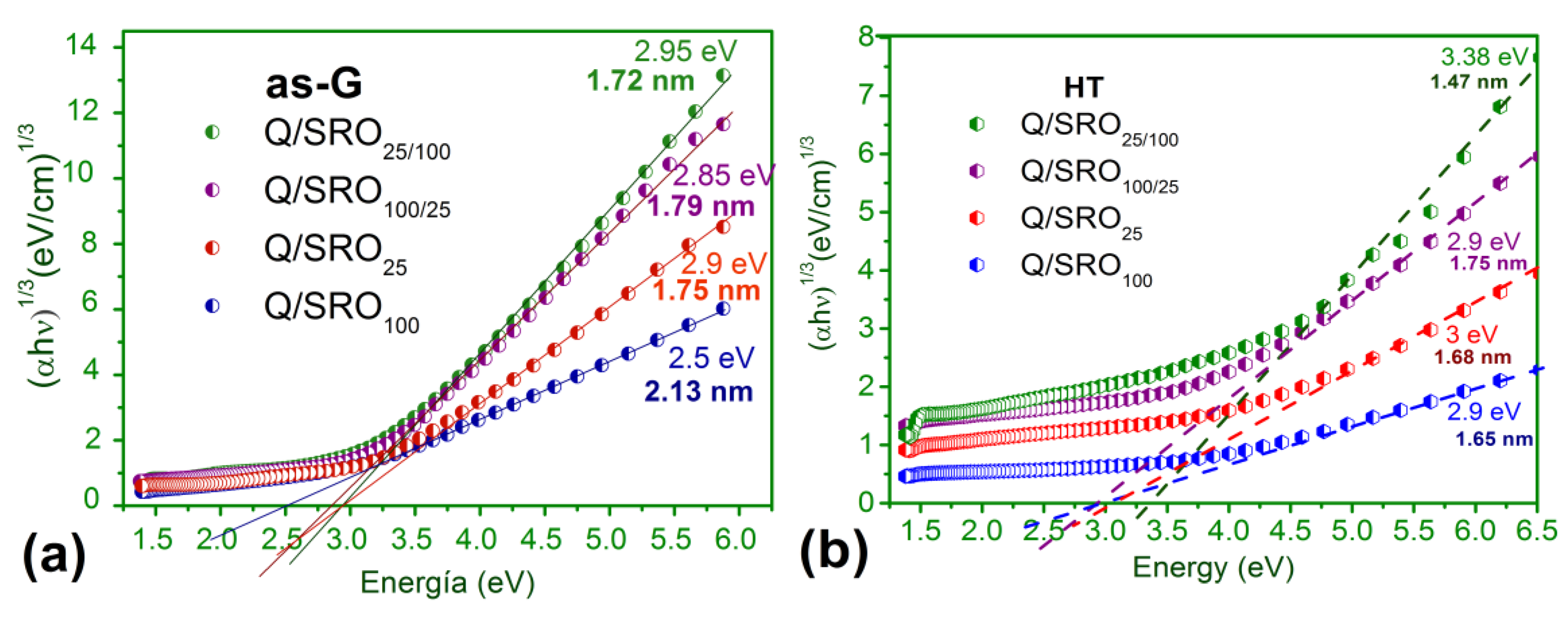
| Sample | As-Grow | H-T | ||
|---|---|---|---|---|
| Q-Quartz | Egopt (eV) of the SRO Films | Diameter (d) of the NC-Si (nm) | Egopt (eV) of the SRO Films | Diameter (d) of the NC-Si (nm) |
| QSRO25 | 2.90 | 1.75 | 3.00 | 1.68 |
| QSRO100 | 2.50 | 2.13 | 2.97 | 1.65 |
| QSRO25/100 | 2.95 | 1.72 | 3.38 | 1.47 |
| QSRO100/25 | 2.85 | 1.79 | 2.90 | 1.75 |
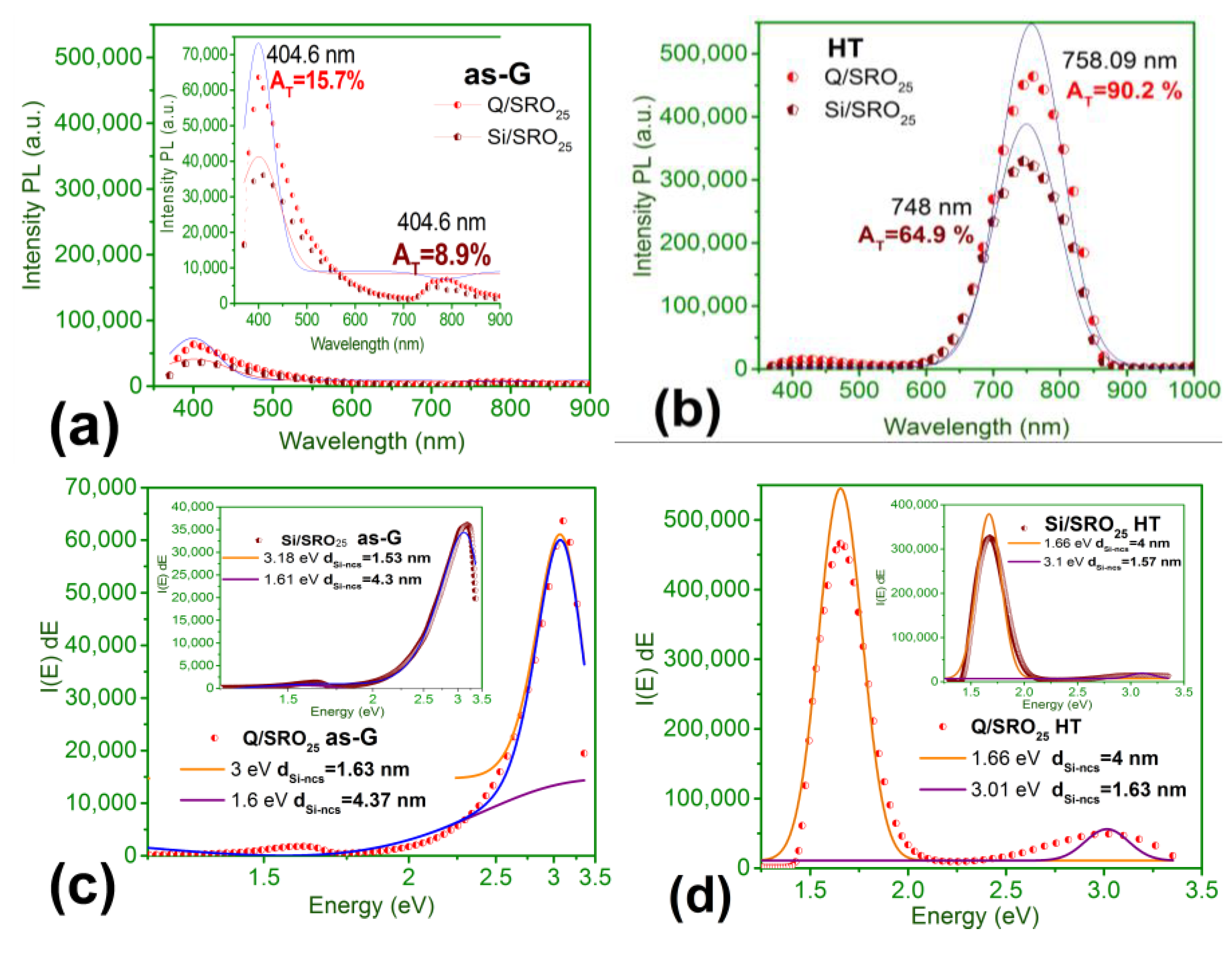
| Sample | Position | Intensity | Nanocrystal Diameter (nm) | Sample | Intensity | Nanocrystal Diameter (nm) | |||
|---|---|---|---|---|---|---|---|---|---|
| as-G | Egopt (eV) | (c.p.s.) | PL | Tauc | HT | Egopt (eV) | (c.p.s.) | PL | Tauc |
| Q25 | 3.00 | 63,951 | 1.63 | 1.85 | Q 25 | 1.63 | 466,185 | 4.18 | |
| Q25 | 1.6 | 2,620 | 4.37 | Q25 | 3.01 | 54,319 | 1.63 | 1.70 | |
| Si 25 | 3.18 | 36,152 | 1.53 | Si 25 | 1.66 | 326,662 | 4.00 | ||
| Si 25 | 1.61 | 1,649 | 4.30 | Si 25 | 3.1 | 18,661 | 1.57 | ||
| Q 100 | 3.1 | 36,414 | 1.57 | 1.62 | Q 100 | 1.72 | 29,486 | 3.72 | |
| Si100 | 2.7 | 55,654 | 1.85 | Q 100 | 3.01 | 90,844 | 1.63 | 1.65 | |
| Si100 | 3.1 | 49,129 | 1.57 | Si 100 | 1.67 | 329,163 | 3.96 | ||
| Q 25/100 | 2.34 | 54,536 | 2.22 | 2.43 | Q 25/100 | 1.53 | 511,742 | 4.82 | |
| Q 25/100 | 2.95 | 28,750 | 1.66 | Q 25/100 | 3.01 | 129,289 | 1.63 | 1.49 | |
| Si 25/100 | 2.37 | 663,686 | 2.19 | Si 25/100 | 1.67 | 327,345 | 4.81 | ||
| Q 100/25 | 2.53 | 61,786 | 2.00 | 1.85 | Si 25/100 | 3.08 | 83,362 | 1.58 | |
| Q 100/25 | 2.99 | 42,253 | 1.64 | Q 100/25 | 1.54 | 333,988 | 4.81 | ||
| Si 100/25 | 2.66 | 57,715 | 1.88 | Q 100/25 | 2.96 | 140,599 | 1.66 | 1.70 | |
| Si 100/25 | 2.92 | 64,215 | 1.68 | Si 100/25 | 1.66 | 327,291 | 2.94 | ||
| Si 100/25 | 3.2 | 49,325 | 1.52 | Si 100/25 | 3.08 | 77,253 | 1.58 | ||
| Samples | As-Grow | Sample | Heat-Treated | ||||
|---|---|---|---|---|---|---|---|
| Substrates | Position (nm) | Intensity (A.U.) | AT (%) | Substrates | Position (nm) | Intensity (A.U.) | AT (%) |
| Si/SRO25/100 | 536.2 | 61,574.7 | 19.1 | Q/SRO25/100 | 814.2 | 509,139.7 | 100.0 |
| Q/SRO25/100 | 554.4 | 54,882.6 | 18.7 | Q/SRO25 | 758.09 | 462,931.5 | 90.2 |
| Q/SRO100/25 | 513.7 | 61,914.2 | 16.8 | Q/SRO100/25 | 812 | 332,546.4 | 73.0 |
| Q/SRO25 | 404.6 | 63,951.6 | 15.7 | Si/SRO25/100 | 753.2 | 324,098.8 | 67.2 |
| Si/SRO100/25 | 469.6 | 61,965.4 | 15.4 | Si/SRO100 | 748 | 330,469.0 | 65.7 |
| Q/SRO100 | 453.4 | 54,617.9 | 13.6 | Si/SRO25 | 509.9 | 327,256.6 | 64.9 |
| Si/SRO100 | 405.1 | 39,220.4 | 9.6 | Si/SRO100/25 | 751.6 | 323,288.0 | 62.7 |
| Si/SRO25 | 404.6 | 63,808.1 | 8.9 | Q/SRO100 | 727 | 91,324.5 | 31.7 |
| Position | Mechanisms of Emission |
|---|---|
| From 1.77 to 1.24 eV Infrared [3,13] | (CLI) Luminescent centers located in the nc-Si/SiO2 Interface |
| From 1.99 to 1.77 eV Red [13,17] | (QC) Quantum Confinement effect with the interaction of the nc-Si interface and the oxide matrix. |
| From 2.2 to 1.99 eV Orange and Red [13,31] | (NBOHC) and E′ centers ≡Si−O•O≡Si+ Non-Bridge Oxygen Hole Center |
| From 2.51 to 2.07 eV Green and Yellow [3,13,31] | (Eδ′) Positively charged Oxygen vacancies |
| From 2.72 to 2.51 eV Blue [3,13,17] | (NOV) (O ≡Si-Si ≡O) Neutral oxygen Vacancies |
| From 3.17 to 2.72 eV Violet [3,13,31] | (WOB) Weak Oxygen Bonds |
© 2020 by the authors. Licensee MDPI, Basel, Switzerland. This article is an open access article distributed under the terms and conditions of the Creative Commons Attribution (CC BY) license (http://creativecommons.org/licenses/by/4.0/).
Share and Cite
Martínez Hernández, H.P.; Luna López, J.A.; Hernández de la Luz, J.Á.D.; Luna Flores, A.; Monfil Leyva, K.; García Salgado, G.; Carrillo López, J.; Ordoñez Flores, R.; Pérez García, S.A.; Hernández Simón, Z.J.; et al. Spectroscopic and Microscopic Correlation of SRO-HFCVD Films on Quartz and Silicon. Crystals 2020, 10, 127. https://doi.org/10.3390/cryst10020127
Martínez Hernández HP, Luna López JA, Hernández de la Luz JÁD, Luna Flores A, Monfil Leyva K, García Salgado G, Carrillo López J, Ordoñez Flores R, Pérez García SA, Hernández Simón ZJ, et al. Spectroscopic and Microscopic Correlation of SRO-HFCVD Films on Quartz and Silicon. Crystals. 2020; 10(2):127. https://doi.org/10.3390/cryst10020127
Chicago/Turabian StyleMartínez Hernández, Haydee Patricia, José Alberto Luna López, José Álvaro David Hernández de la Luz, Adan Luna Flores, Karim Monfil Leyva, Godofredo García Salgado, Jesús Carrillo López, Rafael Ordoñez Flores, Sergio Alfonso Pérez García, Zaira Jocelyn Hernández Simón, and et al. 2020. "Spectroscopic and Microscopic Correlation of SRO-HFCVD Films on Quartz and Silicon" Crystals 10, no. 2: 127. https://doi.org/10.3390/cryst10020127