Article

Effects of the Domain Wall Conductivity on the Domain Formation under AFM-Tip Voltages in Ion-Sliced LiNbO3 Films

Shubnikov Institute of Crystallography of FSRC “Crystallography and Photonics” RAS, 119333 Moscow, Russia
*
Author to whom correspondence should be addressed.
Crystals 2020, 10(12), 1160; https://doi.org/10.3390/cryst10121160
Submission received: 1 December 2020 / Revised: 15 December 2020 / Accepted: 16 December 2020 / Published: 19 December 2020
(This article belongs to the Special Issue New Trends in Lithium Niobate: From Bulk to Nanocrystals)

Abstract

:
The specified domain patterns were written by AFM-tip voltages in LiNbO3 films composing LNOI (LiNbO3-on-insulator). The domain wall conductivity (DWC) was estimated in the written patterns. This estimate was based on the effects of load resistors RL inserted between DWs and the ground, on the features of occurring domains. In this case, the domain formation is controlled by the ratio between RL and the DWs’ resistance RDW. Starting from the comparison of patterns appearing at different RL, the value of RDW in a specified pattern was estimated. The corresponding DWC is of σDW ≈ 10−3 (Ohm cm)−1 which exceeds the tabular bulk conductivity of LiNbO3 by no less than twelve orders of magnitude. A small DW inclination angle of (10−4)0 responsible for this DWC is not caused by any external action and characterizes the domain frontal growth under an AFM-tip voltage.

Graphical Abstract

1. Introduction

Ferroelectric materials have undergone a renaissance in the last two decades due to the discovery of many novel applications based on micro- and nanosized ferroelectric domains. The main examples of these applications are the nonlinear optical-frequency conversion [1] and an ultrahigh-density data storage [2]. More recently, interest has centered on the conductivity of charged domain walls (CDWs) which is a fundamental property of ferroelectric domains. The authors of [3] were the first to discuss the screening effects at the boundary of “encountering” (“head-to-head”) 180°-domains. The specificity of ferroelastic (twin) domain walls (DWs) was discussed in the pioneering works of Salje and co-authors, e.g., [4,5]. Particularly, the superconductivity at DWs in weakly reduced WO3 and trapping of O-vacancies by DWs in CaTiO3 was reported in [4] and [5], respectively. Later on, an enhanced domain-wall conductivity (DWC) up to the superconductivity was observed in a large amount of ferroelectric films and crystals; the detailed bibliography can be found in several reviews [6,7,8]. Taking into account a small DW thickness and a spatial mobility of ferroelectric domains, CDWs can be regarded as the field controlled nanosized wires. In the context of various applications, a concept of “DW nanoelectronics” was proposed by Catalan and coauthors [7].
DWC is caused by a DW inclination with respect to the direction of spontaneous polarization Ps and subsequent accumulation of a screening charge with the density of σ = 2Ps sinθ (where θ is the DWs’ inclination angle). The authors of [9] for the first time proved experimentally the relation of DWC to the DW inclination angle in LiNbO3 crystals. In the recent TEM experiments [10], an essential meandering of 180° DWs has been found in PPLN, which predicts the appearance of DWC even at non-inclined DWs; for this case, the 2D resistor network approach was proposed [11].
The largest part of DWC studies were performed in LiNbO3 [9,10,11,12,13,14,15], which is the most convenient object for these investigations not only because of its practical potentials, but due to the fact that domain patterns fabricated in this material by any technique, are stable.
The pioneering work [9] concerning the specified DWC in LiNbO3 was mentioned above. The authors of [12] succeeded in enhancing DWC in LiNbO3 by 3–4 orders of magnitude compared to [9], by means of the DWs’ field shaping in combination with a photoactive illumination. In [14] DWC was measured in the domain patterns with a specified DW inclination angle, written by AFM-tip voltages in LiNbO3: 5% Mg plates.
The results described below were obtained in the domain patterns fabricated by AFM-tip voltages in LiNbO3 films forming LNOI (LiNbO3-on-insulator). For the further discussion, we dwell shortly on this device. The comprehensive bibliography can be found, e.g., in the reviews [8,16,17,18]. LNOI (schematically presented in Figure 1a) consists of an ion-sliced single-crystal single-domain LiNbO3 film bonded on an insulating substrate (thin SiO2 layer in our case); this sandwich is fixed onto a LiNbO3 plate. In the LNOI samples under investigations, a thin metal layer serving as an electrode is inserted between LiNbO3 film and SiO2. Recently, we presented the AFM -tip domain writing in LiNbO3 films forming LNOI [19,20] and DWC measurements in the written patterns [13]. Later on, AFM domain writing in LNOI and DWC observations in the written patterns were reported in [15,21,22].
According to the general concept, DWs represent regions of charge accumulation. As a result, an electrostatic repulsion between the closely spaced domains can be expected. Actually, some experimental data provide indirect evidence for this effect. When AFM domain writing in thin LiNbO3 crystals, the neighboring domains became unstable [23] as the inter-domain distance Λ was reduced. Similarly, when AFM domain writing in He-LiNbO3 optical waveguides, the domain sizes tended to decrease as Λ was decreased [24]. An instability and chaotic behavior observed in the domain patterns written by AFM-tip voltages in relatively thick LiNbO3 films [25], can be attributed to an inter-domain electrostatic repulsion.
One can expect that an electrostatic repulsion should be suppressed by the DWs’ grounding leading to the elimination of accumulated charge. This effect was actually observed when AFM domain writing in LNOI [20]. If the metal layer was grounded when writing, the written patterns were regular and stable. Oppositely, if the metal layer was disconnected from the ground, the formed patterns were chaotic and unstable.
For clarity, the further reasoning underlying the problem setting is illustrated by Figure 1b. A domain pattern can be regarded as a system of conducting nanowires with a resistance RDW, embedded into an insulating matrix. Two abovementioned extreme scenarios, namely, the regular and chaotic patterns occurring at RL = 0 and RL = ∞, can be interpreted as the results of grounding DWs and their disconnection from the ground, respectively.
The aim of the present research was to examine an “intermediate” case, namely, the domain formation in the conditions of RDW grounding through a load resistor RL ≠ 0 (Figure 1b). It was expected that the characteristics of the occurring domain patterns will be affected by RL insertion, the effects being controlled by the ratio between RDW and RL.
Experiments were performed in LNOI samples provided by NANOLN Electronics (Jinan, China).

2. Experimental Results

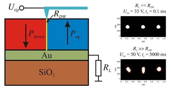
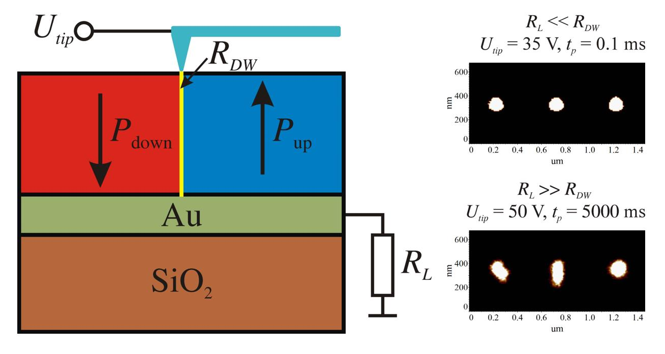
2.1. The Effects of RL Insertion on the Domain Formation

The panels shown in Figure 2a–c, present the phase PFM images of the patterns written at different conditions. One can detect three types of scenarios, depending on the writing conditions.
Let us start from the writing at RL = 0 (Figure 2a). In accordance with our recent results [19,20], domains appear on applying certain threshold Utip. At Utip lower than the threshold, no domains are detected obviously because of the backswitching.
In 500 nm thick films the threshold Utip of the domain appearance is of 18 V; for thicker films it is somewhat larger. Figure 2a presents the results of writing at tp = 0.1 ms, Utip = 35 V. Qualitatively similar panels are visualized on writing in the ranges of Utip > 22 V and tp ≥ 0.1 ms (the shortest experimental tp). The exposure characteristics of the domain diameter D(Utip) and D(tp) were presented in [19]. In agreement with [19,20], the written domains are fully stable. The dependences of the domain sizes D(Utip) and D(tp) are not affected by the inter-domain spacing. A specific feature of these patterns is the domain merging as the distance between the neighboring DWs is decreased (the upper rows in Figure 2a). This merging ignores the domain sizes and occurs when the distance between the neighboring DWs becomes lesser than 20–30 nm. The domain merging phenomenon was described in detail in our preceding publications [19,20].
We dwell shortly on the “pre-threshold” Utip range from 18 to 22 V (Figure 2b) (RL = 0). Figure 2b gives an example of panel written at Utip = 20 V, tp = 500 ms. The appearing domains are unstable since on turning-off Utip, the domain diameter D is slowly shrinking during hours. At the smallest Λ = 100 nm (the upper row in Figure 2b) the domain sizes become somewhat irregular.
The insertion of load resistors RL leads to the following results. Up to certain RL value denoted below as Rcrit, the scenario is very similar to that observed at RL = 0, the writing conditions being the same (Figure 2a). At RL > Rcrit the writing characteristics change abruptly (Figure 2c). Now, to create a stable pattern with the domain sizes close to those observed at RL = 0 under the same Utip, the exposure time should be increased up to seconds, which exceeds tp required for writing at 0 ≤ RL ≤ Rcrit more than by order of magnitude.
Let us discuss in order the phenomena described. In further consideration an ohmic contact between DWs and the metal layer was assumed.
A written pattern shorted to the metal layer, in its turn grounded through a resistor RL can be represented jointly by an equivalent circuit consisting of two resistors, RDW and RL, connected in series (Figure 1b); here RDW is the total DWs resistance. As the resistance of the surrounding crystal bulk is by orders of magnitude larger than RDW, the voltage drop on it is neglected.
The phenomena occurring at RL = 0 can be qualitatively accounted for by the elimination of an inter-domain repulsion due to the DW’s grounding. As a result, the times required for the formation of an equilibrium domain structure are rather short. Due to the disappearance of an inter-domain electrostatic repulsion, nothing prevents the domains from merging when they come together. The physical meaning of the critical distance of 20–30 nm between the neighboring DWs at which the domains start to merge, is unclear yet.
As follows from Figure 1b, at RL≠ 0 the domain formation is governed by the ratio between RL and RDW. Provided that RDW ≥ RL, the voltage drop occurs mainly on RDW; oppositely, in the case that RL ≥ RDW, the voltage drops dominantly on RL. Therefore, in the latter case to write a pattern with the same characteristics as at RL = 0, the exposure times should be increased essentially. This is actually observed in the case illustrated by Figure 2c. At Utip = 35 V, RL = 0 the exposure times of writing are of tenth of seconds, whereas when inserting RL = 1010 Ohm, tp becomes of the order of seconds.
In the framework of our consideration, a threshold change in the domain formation takes place at Rcrit ≈ RDW. In other words, at RL = Rcrit the voltage is divided approximately equally between RL and RDW. It should be taken into account (see the experimental procedure) that when writing any next panel, the value of RL was changed by an order of magnitude. Due to this, the switch from the scenario illustrated by Figure 2a to that shown in Figure 2c occurs in a step-like manner. Therefore, for a given domain pattern, Rcrit can be evaluated within an order of magnitude.
We dwell briefly on the domain formation in the “pre-threshold” voltage range Utip = 18–20 V (Figure 2b). The observed instability of domain patterns can be qualitatively accounted for by the fact that these voltages are insufficient to provide a complete grounding, so an inter-domain repulsion still persists. This qualitative explanation is supported by the fact that the threshold Utip at which the writing characteristics change abruptly, grows with the film thickness being of 22 and 25 V for the 500 and 700 nm thick films, respectively. Note, an instability of AFM written domains in LNOI mentioned in [21], might be related to a non-complete grounding.
Summing up this section, a load resistor Rcrit at which the results of writing change radically (from the panel 2a to 2c), is of the order of magnitude of DWs’ resistance RDW. This approach paths the way to estimate RDW in a given domain pattern by investigating the dependence of the occurring domain structures on the inserted resistors RL.
The following remark is relevant here. Our consideration was illustrated by Figure 2a–c presenting the static ultimate structures. These structures result from the process, involving various stages, the slowest of which being obviously the screening of the bound charge by the free carriers. It occurs within a time of τM =εε0/σ (where εε0 and σ are the dielectric permittivity and conductivity, respectively). Taking the obtained below DW conductivity σ ≈ 2 × 10⁻⁷ (Ohm cm)−1 and ε33 ≈ 30 for LiNbO3, we come to τM ≈ 10−7 s. Therefore, the final DWs’ equilibrium (static) state visualized by the PFM scanning is attained within the times by three orders shorter than the shortest exposure times tp.

2.2. DWC Estimation Based on the Examination of Domain Patterns

A simplified reasoning presented above, paves the way to evaluate DWC in a given domain pattern. It can be done by investigating the effects of specified resistors RL inserted between the metal layer and the ground, on the domain formation. In this section we present an example of this evaluation.
These experiments were performed by writing a row of circled domains by means of step-by-step AFM-tip movement. Figure 3a,b present, respectively, the amplitude PFM image of a fragment of this row and the scanline of an individual domain. The domains were written by Utip = 27 V, tp = 500 ms; the specified distance between the writing points was of Λ = 100 nm.
The sequence of these measurements was the same as when writing the domain panels discussed above. First, the domain row was written at RL = 0 (the reference case). Then, the writing procedure was repeated with the inserted load resistors RL ≠ 0, at each subsequent writing step RL being raised by an order of magnitude. Up to RL = 109 Ohm the shape of the PFM image (illustrated by Figure 3a) remained almost unchanged. At RL = 1010 Ohm a drastic change of the writing conditions was observed, namely to write a row identical to that shown in Figure 3a, tp should be increased up to several seconds, thus more than at ten times. In the framework of our consideration this jump takes place at RL exceeding RDW. Summing up, in the given pattern RDW ≈ RL = 109 Ohm (correct to first order).

3. Discussion

This section consists of two parts. First, for the pattern shown in Figure 3, the DW conductivity σDW was calculated based on the above experimental estimate RDW ≈ 109 Ohm. Second, the DW inclination angle in the pattern shown in Figure 3 was evaluated in the framework of the approach proposed in [14].

3.1. DWC Calculations

Two independent approaches were used to calculate DWC. The first approach is as follows. A single domain can be represented by a cylinder with the diameter D; a DW is represented by a thin-walled tube with the wall thickness of w. The domains written by the Utip amplitudes large enough, penetrate through the whole film thickness, thus the tube length is taken equal to the film thickness L. The resistance of a cylindrical domain with the DW thickness of w can be presented as:
RDW = ρDW (L/πDw) ≡ 1/σDW (L/πDw)
As shown above, the conditions of the domain appearance change radically at certain load resistor Rcrit. In the framework of our consideration it is equal to RDW (correct to first order). From this it follows:
σDW = L/(πDwRcrit)
(for the notations see above).
All terms in this equation are specified except for the value of DW thickness w, which requires to be discussed in more detail. For different materials, e.g., BFO, BTO, and PZT, the value of w ≈ 10 nm was reported repeatedly (for references see [8]). In our measurements, to find this value, we used a tip with r ≤ 10 nm for the PFM scanning. This small tip radius permitted us to improve the accuracy of the DW’s thickness estimation. The repeated measurements in varied domain patterns analogous to that shown in Figure 3a, gave an average value of w ≈ 20 nm with the error of 10%. This value is in line with the literature data mentioned above [8].
Substituting Rcrit = 109 Ohm, L = 500 nm, D = 100 nm, w = 20 nm to Equation (2) we obtain σDW = 8 × 10⁻⁴ (Ohm cm)−1. This estimate of DWC is conservative, since for DW thicknesses lesser than 20 nm, σDW would be larger.
We now turn to the alternative estimation of σDW, which is based on the approach proposed in [14]. The tip contact is considered as a point contact width d. The lines of the current density are curving and spreading out of the DW plane when moving away from the upper electrode. Then:
RDW = ρDW (F/w) ≡ (1/σDW)(F/w)
where F is a dimensionless factor governed by the contact geometry; other notations see above. According to [14], the dependence of F on the contact geometry is satisfactorily approximated by a logarithmic function:
F = 0.72⋅lg(5L/a) ≈ 0.72⋅lg(5L/Rtip)
where a is the point contact width.
As was shown above, Rcrit = RDW. Taking into account Equation (4) we obtain:
σDW = F/(wRcrit) ≈ 0.72⋅lg(5L/Rtip)/(wRcrit)
Substituting into Equation (5) the values used above for calculations by Equation (2) (Rcrit = 109 Ohm, L = 500 nm, Rtip= 35 nm, w = 20 nm) we obtain σDW = 7 × 10⁻⁴ (Ohm cm)−1. This is very close to the above alternative estimate σDW = 8 × 10⁻⁴ (Ohm cm)−1. The value of σDW obtained by two methods exceeds the tabular bulk conductivity of LiNbO3 not less than by twelve orders of magnitude.

3.2. The DW Inclination Angle

We now evaluate the DW inclination angle θ responsible for the σDW value estimated above. In these simplified calculations we follow [14]. The conductivity is expressed as σ = neµ, where n is the screening charge concentration, e is the elementary charge and µ is the charge mobility; so n = σ/eµ. Taking µ ≤ 10−2 cm2/Vs and substituting it together with σDW ≈ 8 × 10⁻⁴ (Ohm cm)−1 into the expression for the concentration of compensating electrons, we obtain n ≥ 0.6 × 1016 cm−3. The inclination angle θ required to provide this compensating charge is calculated from the expression new = 2Ps sinθ [14]. Substituting n ≥ 0.6 × 1016 cm−3, w = 20 nm and Ps = 70 µC cm−2 to this expression, we obtain an inclination angle of θ ≈ (7 × 10⁻³)°. The validity of this estimate is supported by the results of [14], underlying our consideration. In that work, the calculations were performed for the angle θ ≈ 1° specified experimentally. As seen, the inclination of DWs in our case is by orders of magnitude lesser than the angles achieved with the aid of various experimental tricks (e.g., [9,12,14]). A negligible smallness of θ finds the following obvious explanation. As opposed to the aforementioned works aimed at rising DWC by increasing θ, in our case a domain was growing without any external action, so to say, “on its own”. Assuming the frontal DW motion to be the dominant mechanism of the domain growth, the DWs’ inclination angle is governed by the axial field distribution. So, the value of θ specified by the domain frontal growth itself, should be very small. Certain analogy can be drawn with the electron-beam EB domain writing in LiNbO3 [26]. In that case the domains were growing axially under a local field created by EB-irradiation of the polar plane. The DWs in the formed domains appeared to be inclined by a very small angle.

4. Materials and Methods

The samples under study were LNOI wafers composed of a +Z-cut ion-sliced single-domain LiNbO3 film bonded onto SiO2 coated LiNbO3 plate. The film thicknesses in the samples under study were of 300, 500 and 700 nm. The thickness of SiO2 layers was of 1.4 µm. A 100 nm thick Au/Cr layer inserted between the bottom film surface and SiO2 layer, served as an electrode. The total size of the samples was of X × Y × Z = (11 × 9 × 0.5) mm3.
The methods of the domain examination with the aid of scanning probe microscopy are commonly known, so needless to describe them in detail. The only detail should be mentioned. Two types of AFM tips were utilized for different aims. The domain writing and subsequent PFM scanning were performed using Si tip with Pt coating HA_FM/Pt (Tipsnano, Tallinn, Estonia) with the tip curvature radius R ≤ 35 nm. To determine the DWs’ thickness w in the written patterns, we used the Si tips with boron doped diamond coating HA_HR_DCP (Tipsnano) having a tip curvature radius R ≤ 10 nm. All AFM experiments were carried out with a NTEGRA PRIMA SPM system (NT–MDT, Moscow, Russia).
To search for the effects expected, the panels (illustrated by Figure 2) consisting of domain rows with the specified distances Λ between the writing points were written by the stepwise tip movement; in a given row Λ = const. On writing, each next panel was PFM–scanned. Any panel consisting of the domain rows with Λ decreasing from 1000 to 100 nm (bottom-up) was written under constant exposure conditions (Utip = const, tp = const).
When studying the effects of load resistors RL ≠ 0 inserted between the metal layer and the ground on the domain occurrence, the sequence of operations was as follows. First, a reference panel was written under the given writing conditions (Utip = const, tp = const) at RL = 0. Then, the following panels were written with the same Utip and tp, a load resistor RL being inserted between LNOI and the ground. When writing each subsequent panel, the RL value was increased (or decreased) by an order of magnitude. The domain panels written with RL ≠ 0 were compared to the reference one.
The DWC measurements were performed in a row of circled domains written by step-by-step AFM-tip movement (Figure 3a,b). The sequence of these measurements was the same as when writing the domain panels (Figure 2). First, the domain row was written at RL = 0 (the reference case). Then, the writing procedure was repeated with the inserted load resistors RL ≠ 0. At each subsequent writing step, RL was raised by an order of magnitude

5. Conclusions

The main results obtained here can be summarized as follows: The AFM-tip domain writing in LiNbO3 films was investigated under various conditions of the DW’s grounding through the specified load resistors RL inserted between DWs and the ground. The features of arising patterns are determined by the ratio between the domain-wall resistance RDW and RL. The formed patterns depend critically on RL. This permitted us to estimate DWC in a specified pattern. Importantly, this estimate was based on the observations of ferroelectric phenomena. It was performed by comparing the patterns occurring at given Utip and tp with varied RL. The calculations of DWC on the basis of two independent approaches gave the very close values of σDW = (7–8) × 10−4 (Ohm cm)−1. In the framework of the approach developed in [14] this DWC corresponds to a small inclination angle of θ ≈ (7 × 10⁻³)°. The observed DWC not caused by any external manipulation, is related to a DW inclination accompanying the domain frontal growth under an AFM-tip field.
In our opinion, an important general conclusion is as follows: When creating a small-scale domain pattern, no matter by which method, an electrostatic repulsion between the neighboring DWs and, thus, the conditions of DWs’ grounding affect substantially the features of the occurring terminal domain structure.

Author Contributions

R.G. performed the experiments and analyzed the data, T.V. analyzed the data and wrote the paper. All authors have read and agreed to the published version of the manuscript.

Funding

This research received no external funding.

Acknowledgments

The authors are grateful to Boris Sturman for the fair criticism and useful remarks. We are indebted to NANOLN Electronics (Jinan, China) for providing us the LNOI samples. This work was supported by the Ministry of Science and Higher Education of the Russian Federation. The equipment of the Shared Research Center (Project No. RFMEFI62114x0005) was used in experiments.

Conflicts of Interest

The authors declare no conflict of interest.

References

  1. Ferroelectric Crystals for Photonic Applications; Springer Science and Business Media LLC: Berlin/Heidelberg, Germany, 2009; pp. 1–132.
  2. Cho, Y.; Fujimoto, K.; Hiranaga, Y.; Wagatsuma, Y.; Onoe, A.; Terabe, K.; Kitamura, K. Tbit/inch2 ferroelectric data storage based on scanning nonlinear dielectric microscopy. Appl. Phys. Lett. 2002, 81, 4401–4403. [Google Scholar] [CrossRef]
  3. Vul, B.M.; Guro, G.M.; Ivanchik, I.I. Encountering domains in ferroelectrics. Ferroelectrics 1973, 6, 29–31. [Google Scholar] [CrossRef]
  4. Calleja, M.; Dove, M.T.; Salje, E.K.H. Trapping of oxygen vacancies on twin walls of CaTiO3: A computer simulation study. J. Physics Condens. Matter 2003, 15, 2301–2307. [Google Scholar] [CrossRef]
  5. Aird, A.; Salje, E.K.H. Sheet superconductivity in twin walls: Experimental evidence of. J. Physics Condens. Matter 1998, 10, L377–L380. [Google Scholar] [CrossRef]
  6. Seidel, J.; Martin, L.W.; He, Q.; Zhan, Q.; Chu, Y.-H.; Rother, A.; Hawkridge, M.E.; Maksymovych, P.; Yu, P.; Gajek, M.; et al. Conduction at domain walls in oxide multiferroics. Nat. Mater. 2009, 8, 229–234. [Google Scholar] [CrossRef] [Green Version]
  7. Catalán, G.; Seidel, J.; Ramesh, R.; Scott, J.F. Domain wall nanoelectronics. Rev. Mod. Phys. 2012, 84, 119–156. [Google Scholar] [CrossRef] [Green Version]
  8. Bednyakov, P.S.; Sturman, B.I.; Sluka, T.; Tagantsev, A.K.; Yudin, P.V. Physics and applications of charged domain walls. NPJ Comput. Mater. 2018, 4. [Google Scholar] [CrossRef] [Green Version]
  9. Schröder, M.; Haußmann, A.; Thiessen, A.; Soergel, E.; Woike, T.; Eng, L.M. Conducting Domain Walls in Lithium Niobate Single Crystals. Adv. Funct. Mater. 2012, 22, 3936–3944. [Google Scholar] [CrossRef]
  10. Gonnissen, J.; Batuk, D.; Nataf, G.F.; Jones, L.; Abakumov, A.M.; Van Aert, S.; Schryvers, D.; Salje, E.K.H. Direct Observation of Ferroelectric Domain Walls in LiNbO3: Wall-Meanders, Kinks, and Local Electric Charges. Adv. Funct. Mater. 2016, 26, 7599–7604. [Google Scholar] [CrossRef]
  11. Wolba, B.; Seidel, J.; Cazorla, C.; Godau, C.; Haußmann, A.; Eng, L.M. Resistor Network Modeling of Conductive Domain Walls in Lithium Niobate. Adv. Electron. Mater. 2018, 4, 1700242. [Google Scholar] [CrossRef]
  12. Godau, C.; Kampfe, T.; Thiessen, A.; Eng, L.M.; Haußmann, A. Enhancing the Domain Wall Conductivity in Lithium Niobate Single Crystals. ACS Nano 2017, 11, 4816–4824. [Google Scholar] [CrossRef] [PubMed]
  13. Volk, T.; Gainutdinov, R.V.; Zhang, H.H. Domain-wall conduction in AFM-written domain patterns in ion-sliced LiNbO3 films. Appl. Phys. Lett. 2017, 110, 132905. [Google Scholar] [CrossRef]
  14. Werner, C.S.; Herr, S.J.; Buse, K.; Sturman, B.; Soergel, E.; Razzaghi, C.; Breunig, I. Large and accessible conductivity of charged domain walls in lithium niobate. Sci. Rep. 2017, 7, 9862. [Google Scholar] [CrossRef] [PubMed]
  15. Lu, H.; Tan, Y.; McConville, J.P.V.; Ahmadi, Z.; Wang, B.; Conroy, M.; Moore, K.; Bangert, U.; Shield, J.E.; Chen, L.; et al. Electrical Tunability of Domain Wall Conductivity in LiNbO3 Thin Films. Adv. Mater. 2019, 31, e1902890. [Google Scholar] [CrossRef] [PubMed]
  16. Poberaj, G.; Hu, H.; Sohler, W.; Gunter, P. Lithium niobate on insulator (LNOI) for micro-photonic devices. Laser Photon- Rev. 2012, 6, 488–503. [Google Scholar] [CrossRef]
  17. Boes, A.; Corcoran, B.; Chang, L.; Bowers, J.; Mitchell, A. Status and Potential of Lithium Niobate on Insulator (LNOI) for Photonic Integrated Circuits. Laser Photon- Rev. 2018, 12, 1700256. [Google Scholar] [CrossRef]
  18. Rusing, M.; Weigel, P.O.; Zhao, J.; Mookherjea, S. Toward 3D Integrated Photonics Including Lithium Niobate Thin Films: A Bridge Between Electronics, Radio Frequency, and Optical Technology. IEEE Nanotechnol. Mag. 2019, 13, 18–33. [Google Scholar] [CrossRef]
  19. Gaĭnutdinov, R.V.; Volk, T.; Zhang, H.H. Domain formation and polarization reversal under atomic force microscopy-tip voltages in ion-sliced LiNbO3 films on SiO2/LiNbO3 substrates. Appl. Phys. Lett. 2015, 107, 162903. [Google Scholar] [CrossRef]
  20. Volk, T.; Gainutdinov, R.; Zhang, H. Domain Patterning in Ion-Sliced LiNbO3 Films by Atomic Force Microscopy. Crystals 2017, 7, 137. [Google Scholar] [CrossRef]
  21. Shao, G.-H.; Bai, Y.-H.; Cui, G.-X.; Li, C.; Qiu, X.-B.; Geng, D.-Q.; Wu, D.; Lu, Y.-Q. Ferroelectric domain inversion and its stability in lithium niobate thin film on insulator with different thicknesses. AIP Adv. 2016, 6, 075011. [Google Scholar] [CrossRef] [Green Version]
  22. Slautin, B.N.; Turygin, A.; Greshnyakov, E.D.; Akhmatkhanov, A.R.; Zhu, H.; Shur, V.Y. Domain structure formation by local switching in the ion sliced lithium niobate thin films. Appl. Phys. Lett. 2020, 116, 152904. [Google Scholar] [CrossRef] [Green Version]
  23. Kan, Y.; Bo, H.; Lu, X.; Xu, T.; Jin, Y.; Wu, X.; Huang, F.; Zhu, J. Decay properties of artificial two-domain structures in LiNbO3 crystals studied by scanning probe microscope. Appl. Phys. Lett. 2010, 97, 202903. [Google Scholar] [CrossRef]
  24. Ofan, A.; Lilienblum, M.; Gaathon, O.; Sehrbrock, A.; Hoffmann, A.; Bakhru, S.; Bakhru, H.; Irsen, S.; Jr, R.M.O.; Soergel, E. Large-area regular nanodomain patterning in He-irradiated lithium niobate crystals. Nanotechnology 2011, 22, 285309. [Google Scholar] [CrossRef] [PubMed] [Green Version]
  25. Ievlev, A.V.; Jesse, S.; Morozovska, A.N.; Strelcov, E.; Eliseev, E.A.; Pershin, Y.V.; Kumar, A.; Shur, V.Y.; Kalinin, S. Intermittency, quasiperiodicity and chaos in probe-induced ferroelectric domain switching. Nat. Phys. 2013, 10, 59–66. [Google Scholar] [CrossRef]
  26. Dierolf, V.; Sandmann, C. Direct-write method for domain inversion patterns in LiNbO3. Appl. Phys. Lett. 2004, 84, 3987–3989. [Google Scholar] [CrossRef]
Figure 1. The schematic presentation of a domain written by AFM-tip voltage in LNOI (a) and the equivalent circuit of the domain writing (b). In (a) the red vertical lines represent DWs, the horizontal green and yellow layers show the metal and SiO2 ones, respectively; in (b) RDW is the DWs’ total resistance. In (a,b) RL is the load resistor.
Crystals 10 01160 g001
Figure 2. PFM images of the domain panels observed under different conditions of AFM-tip writing. (a) Utip = 35 V, tp = 0.1 ms, RL = 0; almost the same images are observed up to RL = 109 Ohm (see below); (b) Utip = 21 V, tp = 500 ms, RL = 0; (c) Utip = 50 V, tp = 5 s, RL = 1010 Ohm.
Crystals 10 01160 g002
Figure 3. The amplitude PFM image of an AFM-written domain chain underlying the below calculations of DWC (a) and the scanline of an individual domain (marked with a green arrow in PFM image) composing this chain (b); Utip = 27 V, tp = 500 ms; the AFM-tip radius r ≤ 10 nm.
Crystals 10 01160 g003
Publisher’s Note: MDPI stays neutral with regard to jurisdictional claims in published maps and institutional affiliations.

