Article

Influence of Vacancy Defects on the Interfacial Structural and Optoelectronic Properties of ZnO/ZnS Heterostructures for Photocatalysis

1
CAS Key Laboratory of Nanosystem and Hierarchical Fabrication, National Center for Nanoscience and Technology, Beijing 100190, China
2
University of Chinese Academy of Sciences, Beijing 100049, China
*
Author to whom correspondence should be addressed.
Catalysts 2023, 13(8), 1199; https://doi.org/10.3390/catal13081199
Submission received: 30 June 2023 / Revised: 24 July 2023 / Accepted: 8 August 2023 / Published: 10 August 2023

Abstract

:
Hybrid density functional theory has been employed to study the influence of interfacial oxygen (O), sulfur (S) and zinc (Zn) vacancies on the optoelectronic properties of ZnO/ZnS heterostructure. The results show that the O, S, and Zn vacancies can decrease cell volume of the ZnO/ZnS heterostructure, leading to slight deformation from the perfect heterostructure. The quasi-band gap of ZnO/ZnS heterostructure is remarkably reduced compared to the ZnO surface. Hence, the visible light response is enhanced in ZnO/ZnS heterostructure, which can be further improved by creating an interfacial S or O vacancy. Moreover, the removal of S or O atoms can generate lone electrons in the system, which can enhance n-type conductivity of the heterostructure. The O and S vacancies improve the contribution of the atomic orbitals of ZnZnO (Zn atom in ZnO), ZnZnS (Zn atom in ZnS), S and O to the valence band maximum (VB) of the heterostructure; while the Zn-vacancy remarkably improves the contribution of S states to the conduction band minimum (CB). The resultant type-II band alignment and large difference between the migration speed of electrons and holes can efficiently separate the photogenerated electron-hole pairs. The CB edge positions are more negative than the redox potentials of CO2/CO and H2O/H2, and the VB edge positions are more positive than the redox potential of O2/H2O. Hence, all the systems under investigation can be potentially used as efficient photocatalysts for various applications like CO2 reduction and water splitting.

Graphical Abstract

1. Introduction

The environmental concerns and growing demand for energy are the motivations for sustained research in the field of CO2 reduction and water splitting. It is important to explore semiconductor photocatalysts for efficient utilization of solar energy, as semiconductor photocatalysis is a green technology [1]. So far, many semiconductor photocatalysts have been studied extensively, such as TiO2, ZnO and SrTiO3 [2], while the photocatalytic performance still cannot meet the needs of real application due to many reasons including inactive response to visible light. The modification of these materials with noble metals can enhance the activity and reduce charge carrier recombination [3,4,5,6]. ZnO is considered a promising candidate for the utilization of solar energy like photocatalysis and photovoltaics due to its good physicochemical properties, such as large excitation binding energy (about 60 meV), deep-level defects, and tunable band alignments, high aspect ratio and morphology [7,8,9,10]. In addition, ZnO and ZnS are also common in magnetic applications, especially as diluted magnetic semiconductors, for which the role of defects is essential to understand [11]. However, its wide bandgap, narrow photoresponse range and high recombination rate of photogenerated electron-hole pairs limit its photocatalytic performance. Various approaches have been developed to improve light absorption and to suppress the recombination of photogenerated charge carriers, including manipulating exposed facet [12,13,14], loading co-catalysts [14,15,16,17] and fabricating heterojunction structures [1,18,19]. The heterojunction fabrication is a feasible strategy to adjust the electronic and optical properties and to suppress the recombination of photoinduced charge carriers in the semiconductors, resulting in wide applications not just in the photocatalysis, but also in high electron mobility transistors, light-emitting diodes, lasers and solar cell technologies [20,21]. Considering visible light accounts for nearly half of solar energy, the current investigations are thus focused on the heterostructure photocatalysts with visible-light response for CO2 reduction and water splitting.
Zinc chalcogenides belong to the II–VI semiconductors and have received extensive interest in the applications of photocatalysis and photovoltaics [22,23,24]. ZnS is a direct semiconductor with a wide bandgap, which shows great potential to construct ZnO/ZnS core–shell systems in order tprove the light absorption [4]. ZnS/ZnO core-shell nanostructure can be fabricated by in-situ growth of ZnO on ZnS via simple thermal treatment [2]. It is claimed that the Z-scheme charge transfer mechanism can take place in ZnS/ZnO heterostructure, where the photogenerated electrons in the CB of ZnO can recombine with the holes produced in the VB of ZnS. It has also been reported that the transfer of photogenerated charge carriers follows the type-II charge transfer mechanism for the wurtzite-ZnS/ZnO heterostructure, i.e., the electrons transfer from wurtzite-ZnS to ZnO and holes migrate from ZnO to ZnS [3]. The computational study using density functional theory (DFT) is a powerful tool to predict the charge transfer and band alignments of the heterostructures. For instance, ZnO/ZnX (X = S, Se, Te) heterostructures containing two layers of ZnX and six layers of ZnO have been theoretically calculated for applications in solar cells [25]. The designed ZnO/ZnX heterostructures have type-II band alignments, with a respective bandgap of 2.2, 1.71 and 0.95 eV for ZnO/ZnS, ZnO/ZnSe and ZnO/ZnTe. It is also claimed that the calculated bandgap is 2.31 eV for bulk ZnO/ZnS heterostructure and 2.07 eV for core/shell ZnO/ZnS heterostructure nanowires [26]. It is noted that various defects can be readily formed in ZnO, which can have a huge impact on the properties of a heterostructure material containing ZnO.
It has been observed experimentally that the ZnO/ZnS core/shell nanostructure with a thick core of ZnO and a thin ZnS shell shows enhanced photocatalytic properties [27,28]. Hence, ZnO/ZnS heterostructures are constructed by placing two layers of ZnS(001) (ZnS2L, where “L” represents layer) on six layers of ZnO(11 2 ¯ 0) (ZnO6L) to better understand the ZnO/ZnS heterostructure, with the vacancy of oxygen (VO), sulfur (VS) and zinc (VZn) generated at the interface of heterostructure. Hybrid DFT calculations have been performed to study the properties of the obtained heterostructures. The results indicate that the ZnO6L/ZnS2L is a type II heterostructure, which can effectively facilitate the separation of photogenerated charge carriers at the interface and thereby enhance the photocatalytic performance. The optical absorption of ZnO/ZnS heterostructure is remarkably enhanced compared to the isolated ZnO6L and ZnS2L. Moreover, the influence of interfacial vacancies of VO, VS and VZn on the geometric and electronic structure, interfacial charge behavior, band edge position, and optical properties of ZnO/ZnS heterostructure has been thoroughly calculated in this work. The applications of the obtained heterostructures in the photocatalysis are briefly discussed too.

2. Results and Discussion

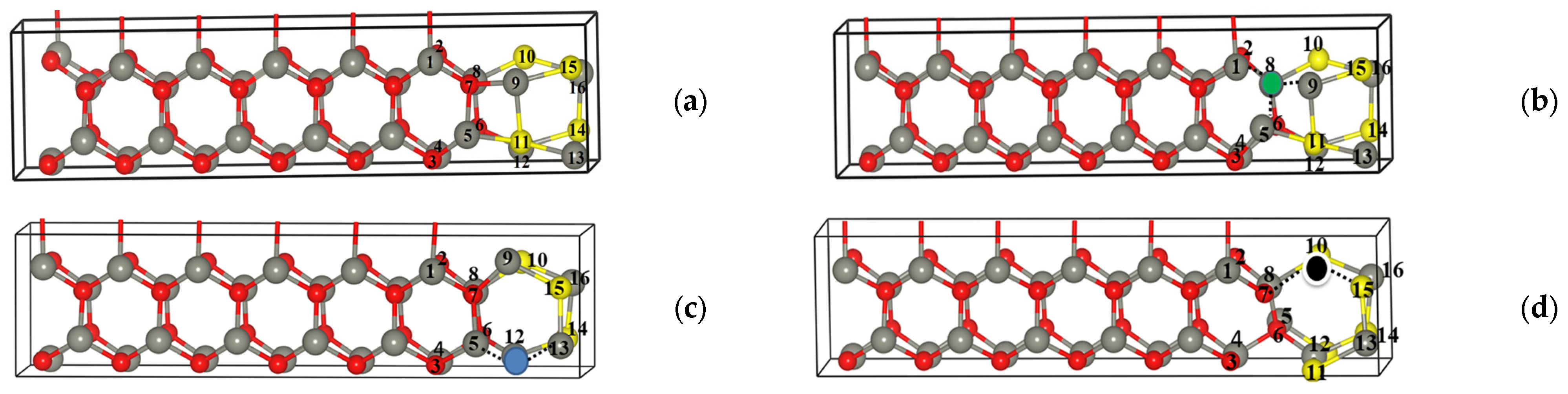
2.1. Geometric Structure of ZnO/ZnS Heterostructures with and without Interfacial Vacancy

Before the investigation on the ZnO/ZnS heterostructures, the lattice structure of bulk wurtzite ZnO, bulk cubic ZnS, ZnO6L and ZnS2L surfaces are explored first. The calculated optimized lattice parameters are a = b = c = 5.44 Å for zinc blend ZnS and are a = b = 3.29 Å, c = 5.29 Å for wurtzite ZnO (Figure S1), which are well consistent with previous theoretical [25,29] and experimental results [30,31], representing that the theoretical approach is reasonable and reliable. Six layers of ZnO(11 2 ¯ 0) and two layers of ZnS(001) facets have been constructed from the bulk-relaxed ZnO and ZnS unit cells (Figure S2). The optimized lattice parameters are a = 5.71 Å and b = 5.34 Å for ZnO6L surface and a = 5.45 Å and b = 5.45 Å for ZnS2L, respectively. The calculated lattice mismatch between ZnO(11 2 ¯ 0) and ZnS(001) facets is 2.6%, indicating small mismatch and good stability (i.e., minute strain) of the designed ZnO/ZnS heterostructure. The ZnO/ZnS slab is optimized after the construction of heterostructure (Figure 1a). The optimized lattice parameters are listed in Table 1. In addition, the thermal stability of the ZnO/ZnS heterostructure is evaluated by calculating the binding energy with equation of Eb = EZnO/ZnSEZnO6LEZnS2L, where EZnO/ZnS, EZnO6L and EZnS2L are the total energies of relaxed ZnO/ZnS heterostructure, ZnO6L and ZnS2L, respectively. The calculated interface binding energy of ZnO/ZnS is –0.92 eV, implying that the obtained heterostructure interface is stable [32].
For the ZnO/ZnS heterostructures with vacancy defects, the VO, VS and VZn vacancies are generated at the interface. The optimized structures of the obtained heterostructures are shown in Figure 1b–d, with indexed serial numbers for the atoms under investigation, and the optimized lattice parameters are listed in Table 1. It is clear that the VO, VS and VZn vacancies decrease the cell volume of ZnO/ZnS heterostructures owing to changes in the positions of atoms around the vacancy, leading to slight deformation in the pertinent structure. A maximum decrease in volume is observed when the Zn9-S11 bridge bond in ZnS region is broken due to the formation of VS and VZn vacancies at the interface of ZnO/ZnS (Figure 1c,d). In such cases, the atoms of ZnS arrange themselves in accordance with the substrate due to the synergistic effect.
In addition, the bond length of those around the vacancy is calculated to further probe the influence of vacancy on the system geometry (Table 2). In the case of VO at the interface, the bond length ranges from 2.0 to 2.41 Å for the bonds of O2-Zn8, Zn8-O6, Zn4-O6, Zn8-S10, Zn11-S5 and Zn12-S11, which is slightly longer than the same bond in perfect heterostructure; while the bond length of S10-Zn16 and Zn9-S11 is slightly shorter than the respective counterpart in a perfect structure. In the case of VS at the interface, the bond length of O3-Zn5, Zn4-O6 and Zn1-O7 is slightly longer than the same bonds in perfect ZnO/ZnS heterostructure; while it is shorter for Zn8-S10, S10-Zn16 and Zn12-Zn14, ranging from 2.01 to 2.42 Å. In the case of VZn at the interface, the respective bond length of Zn8-S10, S10-Zn16, S11-Zn13 and S11-Zn12 is 2.65, 2.60, 2.54 and 2.41 Å, which is longer than the same bonds in perfect structure. Hence, the creation of vacancies at the interface has an impact on the geometrical structure of the ZnO/ZnS heterostructure. The bond strength becomes relatively weaker compared to that in the perfect heterostructure in the case of the elongated bond length and becomes comparatively stronger in the case of the shortened bond length.

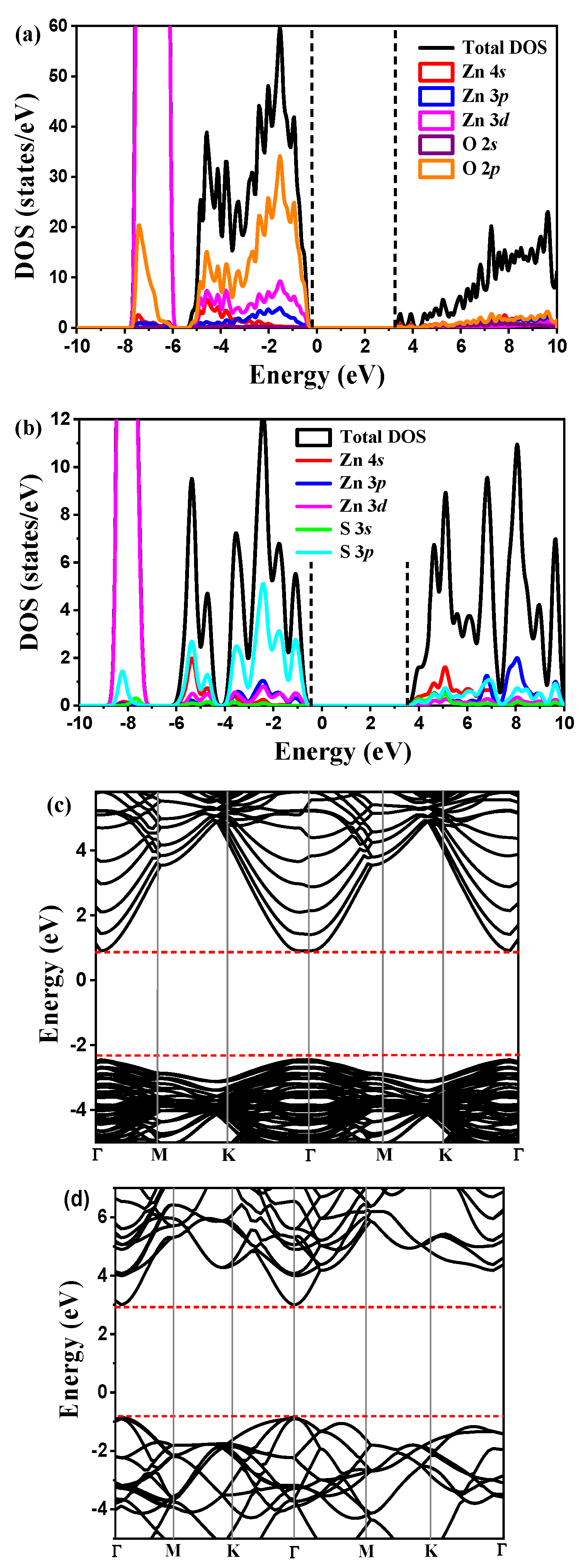
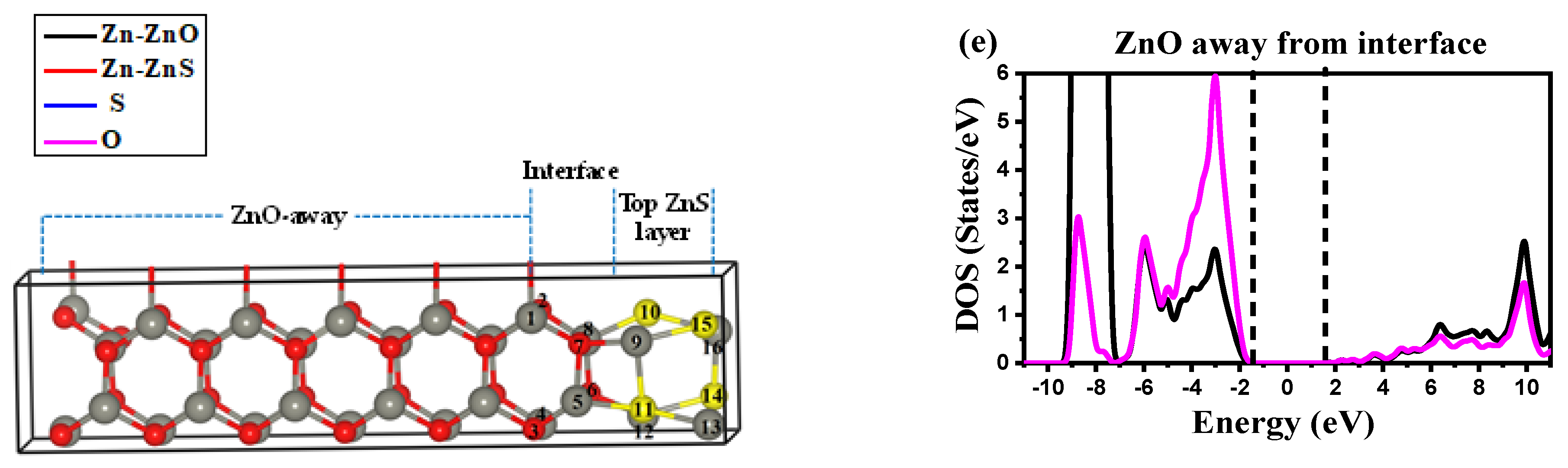
2.2. Electronic Properties of Perfect and Defective ZnO/ZnS Heterostructures

The electronic properties of ZnO/ZnS heterostructures with and without interfacial VO, VS and VZn vacancies are calculated to study the energy bands and interfacial electronic structure. The electronic properties of ZnO6L and ZnS2L are first studied for comparison. The calculated projected density of states (PDOS) and band structures of ZnO6L and ZnS2L are shown in Figure 2. The calculated band structures indicate that the ZnO6L and ZnS2L are direct bandgap semiconductors with respective numerical values of 3.32 and 3.80 eV. The valence band (VB) (–4 to 0 eV) of the ZnO6L surface is mainly contributed by O 2p, Zn 3d, Zn 3p and Zn 4s, and its conduction band (CB) is composed of Zn 4s, O 2s and O 2p states. The total density of states (TDOS) in VB is dominated by S 3p, Zn 3d, Zn 3p and Zn 4s for the ZnS2L, and Zn 4s, S 3s, S 3p and Zn 3p contribute its CB.
The calculated PDOS of whole slabs for the perfect ZnO/ZnS, ZnO/ZnS with interfacial VO (ZnO/ZnS-VO), ZnO/ZnS with interfacial VS (ZnO/ZnS-VS) and ZnO/ZnS with interfacial VZn (ZnO/ZnS-VZn) are shown in Figure 3. In perfect ZnO6L/ZnS2L heterostructure, the upper VB (–4 to 0 eV) is mainly contributed by O 2p, Zn 3d, S 3p, Zn 3p and Zn 4s orbitals, and the CB is mainly contributed by Zn 4s, O 2s, O 2p, Zn 3p, S 3p and S 3s orbitals (Figure 3a). The quasi-bandgap of the ZnO/ZnS heterostructure is 2.24 eV, which is decreased by 1.06 eV compared to the individual ZnO surface due to S 3p states. This is consistent with the theoretical result in the literature for ZnO/ZnS heterostructure [25], as well as with the experimental report for the sample of ZnS monolayer attached to the ZnO [33].
In the case of VO and VS at the interface, the VB is mainly composed of O 2p, Zn 3d, S 3p, Zn 3p and Zn 4s orbitals, and the CB is mainly contributed by Zn 4s, O 2s, O 2p, Zn 3p and S 3p orbitals (Figure 3b,c). The upper VB region (–0.8~0.5 eV) is split as compared with the perfect heterostructure. Such states are more clearly visible in the plots of the local density of states (LDOS), which will be discussed later. Moreover, owing to the downshift of the CB edge, the quasi-band gap is further reduced respectively to 1.78 and 1.87 eV for ZnO/ZnS-VO and ZnO/ZnS-VS. As for the ZnO/ZnS-VZn, the VB is mainly contributed by O 2p, Zn 3d, S 3p, Zn 3p and Zn 4s orbitals, and the CB is mainly composed of Zn 4s, S 3p, S 3s, O 2p, Zn 3p and O 2s orbitals (Figure 3d).
In perfect heterostructure, the p orbital of O and S atoms forms bonds with the neighboring Zn atoms, and the Zn11 atom at the interface is bonded with the neighboring O7 and S15 atoms. Thus, the removal of S or O atom at the interface can create lone electrons in the system that will be thermally excited to the CB, resulting in enhanced n-type conductivity due to the shift of Fermi level toward CB as compared with the perfect heterostructure. The Fermi energy is 1.24 eV in perfect ZnO/ZnS heterostructure, which is increased respectively to 1.58 and 1.71 eV once the VS and VO are generated at the interface (Figure 3b,c). Similarly, the removal of Zn9 atom can create a deficiency of electrons in the system, resulting in the shift of Fermi energy from 1.24 eV for the perfect system to 1.06 eV for the ZnO/ZnS-VZn (Figure 3d).
In addition, Figure 4 shows the calculated LDOS of different parts in all the heterostructures, i.e., the ZnO layer away from the interface (ZnO-away), interface, and top ZnS layer (Figure S3). Clearly, the bandgap of the ZnO-away layer remains the same for all the heterostructures (3.03 eV), i.e., the VO, VS and VZn vacancies have no impact on the electronic structure of ZnO layers away from the interface (Figure 4e). However, the upper VB of interface region (–1.5 to –0.6 eV) is mainly occupied by the TDOS of S atom for the perfect heterostructure (Figure 4a) and is populated by the contribution of Zn atom in ZnO (Zn-ZnO), S atom, Zn atom in ZnS (Zn-ZnS) and O atom for the ZnO6L/ZnS2L-VO and ZnO6L/ZnS2L-VS heterostructures (Figure 4b,c). The TDOS of Zn-ZnO is below the TDOS of the S atom in the upper VB region of the perfect heterostructure, indicating that the orbitals of Zn-ZnO are filled; whereas the orbitals of Zn-ZnS and Zn-ZnO atoms in ZnO6L/ZnS2L-VO and ZnO6L/ZnS2L-VS are partially empty and sit at relatively high energy since a portion of charges in Zn-ZnS and Zn-ZnO atoms transfer to the CB. As in the case of VZn, the CB bottom (1.8 to 3.0 eV) of interface region is mainly composed of TDOS of the S atom (Figure 4d), but with a small contribution from the TDOS of Zn-ZnO, Zn-ZnS and O atoms. Considering the CB for the perfect heterostructure has a very small contribution from the TDOS of S, Zn and O atoms, VZn at the interface remarkably enhances the contribution of S states to the CB.
As for the top ZnS layer, it is found from the LDOS that the respective bandgap of ZnS is 2.32, 2.14, 2.10 and 2.38 eV for the perfect heterostructure, the one with VO, VS and VZn (Figure 4). Moreover, due to presence of VO and VS at the interface, the upper VB of ZnO6L/ZnS2L-VO and ZnO6L/ZnS2L-VS is split as compared to the perfect heterostructure. Hence, VO and VS can influence the electronic structure of the top heterostructure layer. Similarly, VZn also affects the electronic structure of the top ZnS layer in the heterostructure.

2.3. Interfacial Charge Transfer and Bader Charge Analysis

It is noted that the charges will redistribute in the materials once the heterojunction is formed between ZnO6L and ZnS2L. The work function (actually Fermi level) is an important factor for a semiconductor material to be used in photocatalysis [34], which determines the charge transfer at the interface upon the formation of a heterojunction. The work function is defined by the equation of WF = EVacEF, where EVac and EF is the electrostatic potential of an electron at vacuum and Fermi energy, respectively. The planar average electronic potentials with respect to the Z-axis for ZnO6L and ZnS2L surfaces have been calculated by applying dipole correction (Figure 5). The work function is thus calculated to be 5.70 and 5.12 eV for ZnO6L and ZnS2L surfaces, respectively. Therefore, the electrons can transfer from ZnS2L to ZnO6L when they come into contact with each other to form a heterostructure, as the work function of ZnS2L is less than that of ZnO6L.
Moreover, Bader charge calculations [35] have been completed to quantitatively acquire net charge on the atoms at the interface upon the formation of heterostructure (Table 3). The Bader net charges of the interfacial atoms in perfect ZnO/ZnS heterostructure are obtained by taking the difference between total charges on the atoms in a heterostructure and the total charge on atoms in the constituent surfaces. In Figure 6, the atoms above zero (with a positive value) show the accumulation of electrons, and the atoms below zero (with a negative value) mean the loss of electrons. Clearly, the Zn13 and Zn16 atoms at the heterojunction interface gain electrons, and the Zn1, Zn4, Zn5, Zn8, Zn9 and Zn12 atoms lose electrons. The net gain charges are 0.12 e and 0.12 e for Zn13 and Zn16 atoms, respectively. The net loss charges are 0.004 e, 0.02 e, 0.08 e, 0.10 e, 0.17 e and 0.17 e for Zn1, Zn4, Zn5, Zn8, Zn9 and Zn12 atoms, respectively. Meanwhile, the respective charge decreases from 1.22 e, 1.22 e and 1.21 e to 1.21 e, 1.19 e and 1.19 e for O2, O3 and O7 atoms. Thus, the net decrease of charge is 0.01 e, 0.03 e and 0.02 e for O2, O3 and O7, respectively. Similarly, the respective charge increases from 0.87 e, 0.87 e, 0.87 e and 0.87 e to 0.91 e, 0.93 e, 0.91 e and 0.92 e upon the formation of heterojunction for S10, S11, S14 and S15 atoms. Accordingly, the net gain charge is 0.04 e, 0.06 e, 0.04 e and 0.05 e for S10, S11, S14 and S15 atoms, respectively. All these give rise to a total charge transfer of 0.41|e| from the ZnS layer to the ZnO layer.
The Bader charge analysis is further performed to study the change in the total charge of atoms around the vacancy. As in a perfect heterostructure, the S11 atom can make bonds with Zn5, Zn9, Zn12 and Zn13 atoms. Hence, the removal of the S11 atom from the interface can affect the charge of surrounding atoms. The respective total charge reduces from −1.13 e, −0.99 e, −0.99 e and −0.99 e to −0.93 e, −0.72 e, −0.57 e and −0.87 e for Zn5, Zn9, Zn12 and Zn13 atoms in the VS region. Accordingly, the charge of S atoms attached to the Zn and O atoms decreases too. Similarly, the interfacial VO (by removing the O7 atom) also affects the total charge on the Zn atoms around it. The charge decreases from −1.22 e, −1.13 e, −1.11 e and −0.99 e to −0.88, −0.80 e, −0.74 e and −0.78 e for Zn1, Zn5, Zn8 and Zn9, respectively. Moreover, a small decrease is observed in the charge of S atoms attached to the Zn atoms around VO.
In the case of the interfacial VZn, the total charge decreases for the S atoms around VZn. Removal of the Zn atom (Zn9) from the interface reduces the total charge of neighboring S10, S11, S15 and O7 atoms. However, a remarkable change in the total charge of S10 and S11 is observed, i.e., decreasing from 0.90 e and 0.92 e to 0.42 e and 0.49 e, respectively. The decrease in the total charge of S and O atoms around VZn is due to the lack of electrons donated by Zn atoms.

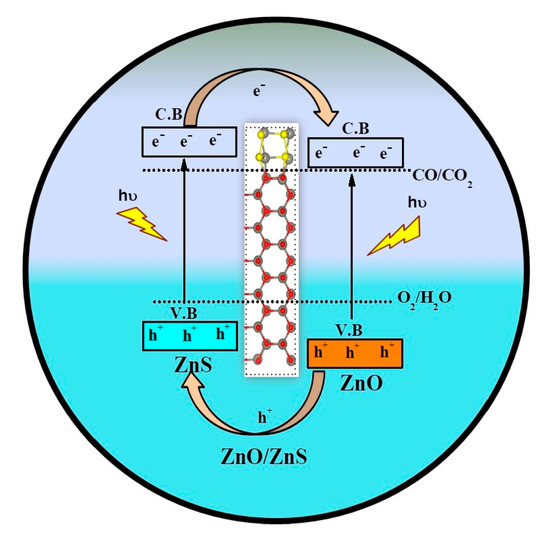
2.4. Band Alignment and Charge Separation of the Heterostructures for Photocatalysis

The photocatalytic performance highly depends on the position of the VB and CB edges of the semiconductors. Using photocatalytic reduction in CO2 as an example, the basic criteria are that the CO2 reduction potential for the specific products must lie between the VB and CB of the heterostructures. The positions of CB and VB edges with respect to the normal hydrogen electrode (NHE) potential can be calculated by using the equations of EVB = χEe + 0.5 Eg and ECB = EVBEg [32], where Ee, Eg and χ is the energy of the free electron (4.5 eV), bandgap, and absolute electronegativity of the semiconductor, respectively. In the perfect heterostructure, the bandgap of the ZnO layer away from the interface is 3.03 eV, which does not change even with the introduction of interfacial VO, VS and VZn to the ZnO/ZnS. The bandgap of the top ZnS layer in the perfect heterostructure is 2.32 eV, and the χ is 5.40 and 5.83 eV for ZnS2L and ZnO6L, respectively. In the case of VO, VS and VZn at the interface, the bandgap of the top ZnS layer becomes 2.32, 2.14, 2.10, and 2.38 eV, respectively. The χ value for ZnS2L changes to 5.30 and 5.5 eV in the case of VS and VZn, respectively.
It is noted from Figure 7 that the heterostructures of perfect ZnO/ZnS, ZnO/ZnS-VO, ZnO/ZnS-VS and ZnO/ZnS-VZn have type-II band alignments. The band edges of ZnO6L and ZnS2L before the contact are illustrated in Figure S4. The band edge positions of ZnO away from the interface are the same in all heterostructures. The positions of VB and CB edges for ZnO-away in perfect ZnO/ZnS, ZnO/ZnS-VO, ZnO/ZnS-VS, and ZnO/ZnS-VZn heterostructures are calculated to be −0.13 and 2.92 V, respectively. Thus, the CB edge position is more negative than the redox potential of CO/CO2 (−0.07 V vs. NHE at pH = 0). Thus, the reduction in CO2 to CO is thermodynamically feasible. The same is true for the water splitting to generate H2. Moreover, the respective VB position of the ZnS layer changes to 2.06, 1.97, 1.85 and 2.21 V for the perfect ZnO/ZnS, ZnO/ZnS-VO, ZnO/ZnS-VS and ZnO/ZnS-VZn, which are all more positive than the O2/H2O (1.23 V). Hence, all the heterostructures reported here are capable of photo-catalytically reducing CO2 and splitting water.
The optical absorption and separation and utilization of photogenerated charge carriers are important parameters for an efficient photocatalyst [36,37]. The visible light absorption of the heterostructures is remarkably enhanced compared to the isolated ZnO and ZnS surfaces since the value of quasi-bandgap decreases to a value below 3 eV, which is further verified by the calculation results presented in Section 2.5. The separation of photogenerated electrons and holes is further investigated by calculating the effective mass at the CB (me) and VB (mh) of the perfect and defective heterostructures (Table 4). The effective mass of charge carriers is first calculated by using Equation (1), where m*, and Ћ are the effective mass and reduced Planck’s constant respectively, while E(K) is the energy of an electron at wavevector K [38]. The difference in mobility of hole and electron is the key to determining the separation of photogenerated charge carriers. Such difference can be evaluated by taking the relative ratio of the effective mass of electrons to holes (r) [39]. The greater the value of r, the larger the difference in the mobility of photogenerated electrons and holes, resulting in lower recombination of electron/hole pairs. It is found from Table 4 that the value of r is larger than 1 for all the studied systems, meaning that the migration speed of holes is much slower than the electrons due to its large value of effective mass. Thus, the type-II band alignment and large difference between the migration speed of electrons and holes can efficiently separate the photogenerated electron/hole pairs.
m = Ћ 2 ( d 2 E ( K ) d K 2 ) 1
To confirm the above quantitative results, the band decomposed charge density of VB maximum (VBM) and CB minimum (CBM) are calculated for the perfect ZnO/ZnS heterostructure and those with vacancy defects (Figure 8). It is found that the VBM is localized to the ZnS layer for the perfect ZnO/ZnS heterostructure and CBM is localized to the ZnO layer (Figure 8a). Hence, it is expected that the photogenerated electrons and holes can be efficiently separated in the heterostructure, reducing the rate of charge recombination. In the presence of VO, the VBM is slightly delocalized compared to the perfect heterostructure owing to its smaller r value (Figure 8b), which is further delocalized in case of VS due to the smallest r value (Figure 8c); while it is more localized to the ZnS layer for ZnO6L/ZnS-VZn due to the largest r value (Figure 8d), implying efficient separation of charge carriers. The same conclusion can be drawn too by analyzing the (de-)localization of CBM for the perfect and defective heterostructures.
The electrons jump from VB to CB when the heterostructures absorb photons with energy above the quasi-bandgap value, with holes left in VB. The photogenerated electrons in the CB of ZnS transfer to the CB of ZnO through the interface due to type-II band alignment, and the holes in the VB of ZnO move to the VB of ZnS, leading to the accumulation of electrons at the CB of ZnO and holes at the VB of ZnS (Figure 7e). Hence, the electrons in CB of ZnO are available for the photocatalytic reduction reactions, while the holes in VB of ZnS take part in the oxidation reactions.

2.5. Optical Properties

The performance of semiconductor photocatalysts is significantly influenced by the optical absorption behavior of the catalyst, which depends on its electronic structure. Hence, the optical absorption spectra of perfect and defective ZnO/ZnS heterostructures are calculated to investigate the effect of interfacial VO, VS, and VZn defects. The frequency dependence on the dielectric function is calculated, which is expressed as ε = ε1(ω) + iε2(ω) [40]. The real component of the dielectric function is calculated by the Kramers-Kronig transformation, and the imaginary part is calculated by summing the large empty states. Furthermore, the absorption coefficient α(ω) is calculated by using Equation (2) [41]. The optical absorption spectra are thus calculated as a function of photon energy for ZnO6L, ZnS2L, perfect ZnO/ZnS, ZnO/ZnS-VO, ZnO/ZnS-VS and ZnO/ZnS-VZn, as shown in Figure 9.
α ω = 2 ε 1 ( ω ) 2 + ε 2 ( ω ) 2   ε 1 ( ω ) 1 / 2 ω
It is noted from the optical spectra that the isolated ZnS2L and ZnO6L surfaces have very weak absorption in the visible-light region (400~760 nm) due to the wide bandgap (Figure 9a). After the formation of the ZnO/ZnS heterostructure, the absorption edge shifts toward lower photon energy (longer wavelength), which enables the heterostructure to utilize visible light. The absorption of perfect ZnO/ZnS heterostructure is improved, as the optical absorption edge (2.18 eV, synchronizing its bandgap) significantly shifts down by about 0.97 eV compared to the isolated ZnO6L surface (3.15 eV). Hence, the optical absorption of heterostructure is enhanced because of the interlayer coupling between the ZnO and ZnS surfaces. Compared to the perfect heterostructure, the quasi-band gap for those with interfacial VO, VS and VZn further narrows down to 1.88, 1.95 and 2.03 eV, respectively. Thus, the absorption edge of ZnO6L/ZnS2L heterostructures with VO, VS and VZn shifts down by 0.30, 0.23 and 0.15 eV compared to the perfect ZnO6L/ZnS2L heterostructure, implying that all the VO, VS and VZn defects can improve the visible-light absorption of the heterostructures (Figure 9b), which is critical for the photocatalysis.

3. Calculation Methods

Vienna Ab initio Simulation Package (VASP) [42,43] was used to perform the calculation within the framework of DFT with the projected augment wave (PAW) method. The generalized gradient approximation (GGA) of the Perdew-Burke-Ernzerhof (PBE) [44,45] was used to approximate the exchange and correlation potential. A 520-eV cut-off energy was set for the expansion of the plane wave. The forces and energies on each ion were reduced respectively below 0.02 eV/and 10−6 eV to optimize the structures, and then the resultant optimized structures are used to investigate the electronic structures. The interactions between adjacent slabs are eliminated by using a thick layer vacuum. For the optimization, k-points of 3 × 3 × 1 were used, while the electronic structure calculation was performed by using 5 × 5 × 1 k-points. In addition, Gaussian smearing was used for the electronic structure calculations. Heyd Scuseria-Ernzerhof (HSE06) [46] hybrid functional was used to calculate the non-spin-polarized optoelectronic properties of isolated ZnO6L and ZnS2L, as well as the ZnO/ZnS heterostructures. HSE06-based calculated results are very accurate and close to the experimental results. In addition to the optoelectronic properties, the hybrid functional also accurately describes the system geometry [47]. The exchange correlation energy in HSE06 functional is given by Equation (3), where E X   L R , P B E α represents the long-range (LR) part and E X S R α , E X   S R , P B E α are the short-range (SR) part of electron-electron interaction. Similarly, β and α represent the mixing coefficient and screening parameter, respectively. The mixing exchange parameter of 0.375 and screening parameter of 0.20 Å−1 have been tested for the bandgap of ZnO and ZnS, which is 3.30 and 3.87 eV (Figure S5), respectively, consistent well with the experimentally results (3.32 eV for ZnO [48] and 3.82 eV for [49]). Therefore, the mixing exchange parameter of 0.375 and screening parameter of 0.20 Å−1 were adopted in all calculations.
E X C H S E = β E X S R α + 1 β E X   S R , P B E α + E X   L R , P B E α + E C P B E

4. Conclusions

In summary, the hybrid DFT method is used to investigate the influence of interfacial O, S, and Zn vacancies on the geometric and optoelectronic properties of ZnO/ZnS heterostructure. The quasi-bandgap of perfect ZnO/ZnS heterostructure (2.24 eV) reduces by about 1.06 eV in comparison with isolated ZnO surface, which is further reduced upon the creation of interfacial VO, VS and VZn, improving visible-light absorption of the materials. The removal of interfacial S or O atom can generate lone electrons in the system, which can improve n-type conductivity of the heterostructure. The electrons accumulate at the CB of ZnO and holes at the VB of ZnS owing to the type-II band alignment and high value of me/mh, which can effectively separate the photogenerated electron/hole pairs. The CB edge position of ZnO is more negative than the redox potential of CO/CO2 and H2 evolution upon water splitting and the VB edge position of ZnS is more positive than the redox potential of O2/H2O, implying that the heterostructures can be used for photocatalytic CO2 reduction and water splitting. Moreover, the optoelectronic and photocatalytic properties of the heterostructure can be improved by introducing interfacial VO, VS and VZn defects. We envision that this work can help design the photocatalysts with high efficiency.

Supplementary Materials

The following supporting information can be downloaded at: https://www.mdpi.com/article/10.3390/catal13081199/s1, Figure S1. Optimized unit cells of (a) bulk wurtzite ZnO and (b) bulk cubic ZnS, where red, yellow and silver balls represent oxygen, sulfur and zinc atoms, respectively; Figure S2. Optimized structures of (a) ZnO6L and (b) ZnS2L surfaces; Figure S3. ZnO layers away from the interface, interface region and top ZnS layer of (a) perfect heterostructure, and heterostructures with (b) VO, (c) VS and (d) VZn, where red, yellow, silver, green, blue and black balls represent oxygen atom, sulfur atom, zinc atom, VO, VS and VZn, respectively; Figure S4. Schematic diagram of band alignment for ZnS2L and ZnO6L before contact, versus normal hydrogen electrode potential; Figure S1. HSE06 calculated band structures of (a) wurtzite ZnO and (b) cubic ZnS by using mixing exchange parameter of 0.375 and screening parameter of 0.20 Å−1.

Author Contributions

Conceptualization, T.H.; methodology, L.G., T.H. and S.H.; validation, L.G. and S.H.; investigation, S.H.; writing—original draft preparation, S.H.; writing—review and editing, T.H.; supervision, T.H.; funding acquisition, T.H. All authors have read and agreed to the published version of the manuscript.

Funding

This work was supported by the National Natural Science Foundation of China (21972029) and the Strategic Priority Research Program of Chinese Academy of Sciences (XDB36000000). S.H. thanks the China Scholarship Council (CSC) for International Ph.D. Students.

Data Availability Statement

Not applicable.

Conflicts of Interest

The authors declare no conflict of interest.

References

  1. Wang, H.L.; Zhang, L.S.; Chen, Z.G.; Hu, J.Q.; Li, S.J.; Wang, Z.H.; Liu, J.S.; Wang, X.C. Semiconductor heterojunction photocatalysts: Design, construction, and photocatalytic performances. Chem. Soc. Rev. 2014, 43, 5234–5244. [Google Scholar] [CrossRef] [PubMed]
  2. Li, P.; He, T. Common-cation based Z-scheme ZnS@ZnO core-shell nanostructure for efficient solar-fuel production. Appl. Catal. B 2018, 238, 518–524. [Google Scholar] [CrossRef]
  3. AlSalka, Y.; Osama Al-Madanat, O.; Hakki, A. TiO2-based photocatalytic hydrogen production: How to transfer it to an applicable approach. Appl. Catal. A 2023, 662, 119287. [Google Scholar] [CrossRef]
  4. Mohamed, K.M.; Benitto, J.J.; Vijaya, J.J.; Bououdina, M. Recent advances in ZnO-based nanostructures for the photocatalytic degradation of hazardous, non-biodegradable medicines. Crystals 2023, 13, 329. [Google Scholar] [CrossRef]
  5. Ferreira, S.H.; Morais, M.; Nunes, D.; Oliveira, M.J.; Rovisco, A.; Pimentel, A.; Aguas, H.; Fortunato, E.; Martins, R. High UV and sunlight photocatalytic performance of porous ZnO nanostructures synthesized by a facile and fast microwave hydrothermal method. Materials 2021, 14, 2385. [Google Scholar] [CrossRef]
  6. Ombaka, L.M.; McGettrick, J.D.; Oseghe, E.O.; Al-Madanat, O.; Best, F.R.G.; Msagati, T.A.; Davies, M.L.; Bredow, T.; Bahnemann, D.W. Photocatalytic H2 production and degradation of aqueous 2-chlorophenol over B/N-graphene-coated Cu0/TiO2: A DFT, experimental and mechanistic investigation. J. Environ. Manag. 2022, 311, 114822. [Google Scholar] [CrossRef]
  7. Xiao, J.-H.; Huang, W.-Q.; Hu, Y.-S.; Zeng, F.; Huang, Q.-Y.; Zhou, B.-X.; Pan, A.; Li, K.; Huang, G.-F. Facile in situ synthesis of wurtzite ZnS/ZnO core/shell heterostructure with highly efficient visible-light photocatalytic activity and photostability. J. Phys. D 2018, 51, 075501. [Google Scholar] [CrossRef]
  8. Flores, E.M.; Raubach, C.W.; Gouvea, R.; Longo, E.; Cava, S.; Moreira, M.L. Optical and structural investigation of ZnO@ZnS core–shell nanostructures. Mater. Chem. Phys. 2016, 173, 347–354. [Google Scholar] [CrossRef] [Green Version]
  9. De Moura, A.P.; Lima, R.C.; Moreira, M.L.; Volanti, D.P.; Espinosa, J.W.M.; Orlandi, M.O.; Pizani, P.S.; Varela, J.A.; Longo, E. ZnO architectures synthesized by a microwave-assisted hydrothermal method and their photoluminescence properties. Solid State Ion. 2010, 181, 775–780. [Google Scholar] [CrossRef]
  10. Zhang, Y.F.; Guo, Z.Y.; Gao, X.Q.; Cao, D.X.; Dai, Y.X.; Zhao, H.T. First-principles of wurtzite ZnO (0001) and (0001) surface structures. J. Semiconduct. 2010, 31, 082001. [Google Scholar]
  11. Sato, K.; Bergqvist, L.; Kudrnovský, J.; Dederichs, P.H.; Eriksson, O.; Turek, I.; Sanyal, B.; Bouzerar, G.; Katayama, Y.H.; Dinh, V.A.; et al. First-principles theory of dilute magnetic semiconductors. Rev. Mod. Phys. 2010, 82, 1633–1690. [Google Scholar] [CrossRef]
  12. Li, P.; Hu, H.F.; Luo, G.; Zhu, S.; Guo, L.J.; Qu, P.; Shen, Q.; He, T. Crystal facet dependent CO2 photoreduction over porous ZnO nanocatalysts. ACS Appl. Mater. Interface 2020, 12, 56039–56048. [Google Scholar] [CrossRef]
  13. Li, R.G.; Zhang, F.X.; Wang, D.G.; Yang, J.X.; Li, M.R.; Zhu, J.; Zhou, X.; Han, H.X.; Li, C. Spatial separation of photogenerated electrons and holes among {010} and {110} crystal facets of BiVO4. Nat. Commun. 2013, 4, 1432. [Google Scholar] [CrossRef] [Green Version]
  14. Lee, S.L.; Chang, C.J. Recent progress on metal sulfide composite nanomaterials for photocatalytic hydrogen production. Catalysts 2019, 9, 557. [Google Scholar] [CrossRef] [Green Version]
  15. Li, X.; Yu, J.G.; Jaroniec, M.; Chen, X.B. Cocatalysts for selective photoreduction of CO2 into solar fuels. Chem. Rev. 2019, 119, 3962–4179. [Google Scholar] [CrossRef]
  16. Yan, H.J.; Yang, J.H.; Ma, G.J.; Wu, G.P.; Zong, X.; Lei, Z.B.; Shi, J.Y.; Li, C. Visible-light-driven hydrogen production with extremely high quantum efficiency on Pt–PdS/CdS photocatalyst. J. Catal. 2009, 266, 165–168. [Google Scholar] [CrossRef]
  17. Yang, J.H.; Wang, D.G.; Han, H.X.; Li, C. Roles of cocatalysts in photocatalysis and photoelectrocatalysis. Acc. Chem. Res. 2013, 46, 1900–1909. [Google Scholar] [CrossRef]
  18. Tien, T.M.; Chen, E.L. A novel ZnO/Co3O4 nanoparticle for enhanced photocatalytic hydrogen evolution under visible light irradiation. Catalysts 2023, 13, 852. [Google Scholar] [CrossRef]
  19. Jin, X.K.; Chen, J.J.; Chen, F.J.; Duan, H.M.; Wang, Z.Y.; Li, J.H. Solid-state synthesis of ZnO/ZnS photocatalyst with efficient organic pollutant degradation performance. Catalysts 2022, 12, 981. [Google Scholar] [CrossRef]
  20. Dharmadasa, I.; Ojo, A. Unravelling complex nature of CdS/CdTe based thin film solar cells. J. Mater. Sci. Mater. Electron. 2017, 28, 16598–16617. [Google Scholar] [CrossRef] [Green Version]
  21. Kumazaki, Y.; Uemura, K.; Sato, T.; Hashizume, T. Precise thickness control in recess etching of AlGaN/GaN hetero-structure using photocarrier-regulated electrochemical process. J. Appl. Phys. 2017, 121, 184501. [Google Scholar] [CrossRef]
  22. Vaneski, A.; Schneider, J.; Susha, A.S.; Rogach, A.L. Colloidal hybrid heterostructures based on II–VI semiconductor nanocrystals for photocatalytic hydrogen generation. J. Photochem. Photobiol. C 2014, 19, 52–61. [Google Scholar] [CrossRef]
  23. Abrikosov, N.K. Semiconducting II–VI, IV–VI, and V–VI Compounds; Springer: Berlin/Heidelberg, Germany, 2013. [Google Scholar]
  24. Chen, M.-M.; Xue, H.-G.; Guo, S.-P. Multinary metal chalcogenides with tetrahedral structures for second-order nonlinear optical, photocatalytic, and photovoltaic applications. Coord. Chem. Rev. 2018, 368, 115–133. [Google Scholar] [CrossRef]
  25. Flores, E.M.; Gouvea, R.A.; Piotrowski, M.J.; Moreira, M.L. Band alignment and charge transfer predictions of ZnO/ZnX (X = S, Se or Te) interfaces applied to solar cells: A PBE+U theoretical study. Phys. Chem. Chem. Phys. 2018, 20, 4953–4961. [Google Scholar] [CrossRef]
  26. Schrier, J.; Demchenko, D.O.; Alivisatos, A.P. Optical properties of ZnO/ZnS and ZnO/ZnTe heterostructures for photovoltaic applications. Nano Lett. 2007, 7, 2377–2382. [Google Scholar] [CrossRef] [Green Version]
  27. Sadollahkhani, A.; Kazeminezhad, I.; Lu, J.; Nur, O.; Hultman, L.; Willander, M. Synthesis, structural characterization and photocatalytic application of ZnO@ZnS core-shell nanoparticles. RSC Adv. 2014, 4, 36940–36950. [Google Scholar] [CrossRef] [Green Version]
  28. Ranjith, K.S.; Senthamizhan, A.; Balusamy, B.; Uyar, T. Nanograined surface shell wall controlled ZnO-ZnS core-shell nanofibers and their shell wall thickness dependent visible photocatalytic properties. Catal. Sci. Technol. 2017, 7, 1167–1180. [Google Scholar] [CrossRef]
  29. Saha, S.; Pal, S.; Sarkar, P.; Rosa, A.; Frauenheim, T. A complete set of self-consistent charge density-functional tight-binding parametrization of zinc chalcogenides (ZnX.; X = O, S, Se, and Te). J. Comput. Chem. 2012, 33, 1165–1178. [Google Scholar] [CrossRef]
  30. Shannon, R.; Prewitt, C. Effective ionic radii in oxides and fluorides. Acta Crystallogr. B 1969, 25, 925–946. [Google Scholar] [CrossRef]
  31. Dedova, T. Chemical Spray Pyrolysis Deposition of Zinc Sulfide Thin Films and Zinc Oxide Nanostructured Layers; Tallinn University of Technology: Tallinn, Estonia, 2007. [Google Scholar]
  32. Liu, J.J. Origin of high photocatalytic efficiency in monolayer g-C3N4/CdS heterostructure: A hybrid DFT study. J. Phys. Chem. C 2015, 119, 28417–28423. [Google Scholar] [CrossRef]
  33. Lahiri, J.; Batzill, M.J. Surface functionalization of ZnO photocatalysts with monolayer ZnS. Phys. Chem. C 2008, 112, 4304–4307. [Google Scholar] [CrossRef]
  34. Opoku, F.; Govender, K.K.; van Sittert, C.G.C.E.; Govender, P.P. Insights into the photocatalytic mechanism of mediator-free direct Z-scheme g-C3N4/Bi2MoO6(010) and g-C3N4/Bi2WO6(010) heterostructures: A hybrid density functional theory study. Appl. Surf. Sci. 2018, 427B, 487–498. [Google Scholar] [CrossRef]
  35. Tang, W.; Sanville, E.; Henkelman, G. A grid-based Bader analysis algorithm without lattice bias. J. Phys. Condens. Matter 2009, 21, 084204. [Google Scholar] [CrossRef]
  36. Xu, J.J.; Chen, M.D.; Fu, D.G. Study on highly visible light active Bi-doped TiO2 composite hollow sphere. Appl. Surf. Sci. 2011, 257, 7381–7386. [Google Scholar] [CrossRef]
  37. Lin, Y.M.; Shi, H.L.; Jiang, Z.Y.; Wang, G.S.; Zhang, X.D.; Zhu, H.Y.; Zhang, R.Q.; Zhu, C.Y. Enhanced optical absorption and photocatalytic H2 production activity of g-C3N4/TiO2 heterostructure by interfacial coupling: A DFT+U study. Int. J. Hydrogen Energy 2017, 42, 9903–9913. [Google Scholar]
  38. Liu, Y.Y.; Lv, P.; Zhou, W.; Hong, J.W. Built-in electric field hindering photogenerated carrier recombination in polar bilayer SnO/BiOX (X = Cl, Br, I) for water splitting. J. Phys. Chem. C 2020, 124, 9696–9702. [Google Scholar] [CrossRef] [Green Version]
  39. Hussain, S.; Guo, L.J.; Louis, H.; Zhu, S.; He, T. First-principles calculations of Wurtzite ZnS1–xSex solid solutions for photocatalysis. Mater. Today Commun. 2019, 21, 100672. [Google Scholar] [CrossRef]
  40. Hussain, S.; Murtaza, G.; Khan, S.H.; Khan, A.; Ali, M.A.; Faizan, M.; Mahmood, A.; Khenata, R. First principles study of structural, optoelectronic and thermoelectric properties of Cu2CdSnX4 (X = S, Se, Te) chalcogenides. Mater. Res. Bull. 2016, 79, 73–83. [Google Scholar] [CrossRef]
  41. Luo, X.K.; Wang, G.Z.; Huang, Y.H.; Wang, B.; Yuan, H.K.; Chen, H. A two-dimensional layered CdS/C2N heterostructure for visible-light-driven photocatalysis. Phys. Chem. Chem. Phys. 2017, 19, 28216–28224. [Google Scholar] [CrossRef]
  42. Kresse, G.; Furthmüller, J. Efficient iterative schemes for ab initio total-energy calculations using a plane-wave basis set. J. Phys. Rev. B 1996, 54, 11169. [Google Scholar] [CrossRef]
  43. Kresse, G.; Furthmüller, J. Efficiency of ab-initio total energy calculations for metals and semiconductors using a plane-wave basis set. Comput. Mater. Sci. 1996, 6, 15–50. [Google Scholar] [CrossRef]
  44. Ernzerhof, M.; Scuseria, G.E. Assessment of the Perdew-Burke-Ernzerhof exchange-correlation functional. J. Chem. Phys. 1999, 110, 5029–5036. [Google Scholar] [CrossRef] [Green Version]
  45. Grimme, S. Semiempirical GGA-type density functional constructed with a long-range dispersion correction. J. Comput. Chem. 2006, 27, 1787–1799. [Google Scholar] [CrossRef] [PubMed]
  46. Heyd, J.; Scuseria, G.E.; Ernzerhof, M. Hybrid functionals based on a screened coulomb potential. J. Chem. Phys. 2003, 118, 8207–8215. [Google Scholar] [CrossRef]
  47. Pham, A.; Assadi, M.H.N.; Yu, A.B.; Li, S. Critical role of Fock exchange in characterizing dopant geometry and magnetic interaction in magnetic semiconductors. Phys. Rev. B 2014, 89, 155110. [Google Scholar] [CrossRef] [Green Version]
  48. Sabine, M.T.; Hogg, S. The wurtzite Z parameter for beryllium oxide and zinc oxide. Acta. Crystallogr. B 1969, 25, 2254–2256. [Google Scholar] [CrossRef]
  49. Raubach, C.W.; de Santana, Y.V.; Ferrer, M.M.; Longo, V.M.; Varela, J.A.; Avansi, W., Jr.; Buzolin, P.G.; Sambrano, J.R.; Longo, E. Strutural and optical approach of CdS@ ZnS core-shell system. Chem. Phys. Lett. 2012, 536, 96–99. [Google Scholar] [CrossRef] [Green Version]
Figure 1. The optimized structure of ZnO/ZnS heterostructures (a) without and with interface defect of (b) VO, (c) VS and (d) VZn, where red, yellow, silver, green, blue and black balls represent oxygen atom, sulfur atom, zinc atom, VO, VS and VZn, respectively. The atoms are numbered to identify the interfacial atoms.
Catalysts 13 01199 g001
Figure 2. The calculated PDOS of (a) ZnO6L surface and (b) ZnS2L surface, and band structure of (c) ZnO6L surface and (d) ZnS2L surface by using HSE06 functional.
Catalysts 13 01199 g002
Figure 3. PDOS of the whole slabs for (a) perfect ZnO/ZnS, (b) ZnO/ZnS–VO, (c) ZnO/ZnS–VS, and (d) ZnO/ZnS–VZn heterostructures. The vertical red-dashed line denotes the Fermi energy.
Catalysts 13 01199 g003
Figure 4. LDOS of the heterostructures for (a) perfect ZnO/ZnS, (b) ZnO/ZnS–VO, (c) ZnO/ZnS–VS, and (d) ZnO/ZnS–VZn, and (e) LDOS of ZnO layer away from the interface, which is the same in all cases and the one for perfect heterostructure is used as an example here.
Catalysts 13 01199 g004aCatalysts 13 01199 g004b
Figure 5. Calculated electrostatic potentials for (a) ZnO6L and (b) ZnS2L surfaces, where green and black dashed lines denote the Fermi level and vacuum energy level, respectively.
Catalysts 13 01199 g005
Figure 6. The calculated net charge transfer of atoms near the interface region after the formation of bulk ZnO/ZnS heterostructure by Bader charge analysis.
Catalysts 13 01199 g006
Figure 7. Band alignments of heterostructures of (a) perfect ZnO/ZnS, (b) ZnO/ZnS−VO, (c) ZnO/ZnS−VS, and (d) ZnO/ZnS−VZn, along with (e) schematic illustration of interfacial charge transfer.
Catalysts 13 01199 g007
Figure 8. Band decomposed charge density for VBM and CBM of (a) ZnO/ZnS, (b) ZnO/ZnS−VO, (c) ZnO/ZnS−VS, and (d) ZnO/ZnS−VZn heterostructures, where red, yellow, silver, green, blue and black balls represent O atom, S atom, Zn atom, VO, VS and VZn, respectively.
Catalysts 13 01199 g008
Figure 9. Optical absorption spectra of (a) isolated ZnO6L and ZnS2L, and (b) perfect ZnO/ZnS, ZnO/ZnS−VO, ZnO/ZnS−VS and ZnO/ZnS−VZn heterostructures.
Catalysts 13 01199 g009
Table 1. Optimized lattice constants, lattice angles, cell volume, and its variation of ZnO/ZnS heterostructure with and without VO, VS and VZn at interface.
a (Å)b (Å)c (Å)AlphaBetaGammaVolume (Å3)Volume Variation (%)
Perfect5.745.3724.2190.00°90.00°90.00°746.73-
VO at interface5.735.3324.1190.04°90.22°90.40°736.361.4%
VS at interface5.745.3523.5289.85°90.31°89.94°723.073.1%
VZn at interface5.745.3523.9189.78°89.94°87.85°733.181.8%
Table 2. The calculated bond lengths at the interface of perfect ZnO/ZnS heterostructure and defective ZnO/ZnS heterostructures with VO, VS and VZn vacancies.
BondLength (Å)
Perfect(i) O2-Zn8, (ii) Zn8-O6, (iii) O3-Zn5, (iv) Zn4-O6, (v) O6-Zn12, (vi) Zn1-O7, (vii) O7-Zn9, (viii) Zn5-O7, (ix) Zn8-S10, (x) S10-Zn16, (xi) Zn16-S15, (xii) S15-Zn9, (xiii) Zn9-S11, (xiv) Zn11-S5, (xv) S11-Zn13, (xvi) Zn12-S14, (xvii) S14-Zn16, (xviii) Zn12-S11 (i) 2.00, (ii) 2.01, (iii) 1.99, (iv) 1.95, (v) 2.03, (vi) 1.97, (vii) 2.04, (viii) 2.04, (ix) 2.33, (x) 2.50, (xi) 2.32, (xii) 2.38, (xiii) 2.40, (xiv) 2.34, (xv) 2.37, (xvi) 2.50, (xvii) 2.31, (xviii) 2.32
VO at Interface(i) O2-Zn8, (ii) Zn8-O6, (iii) O3-Zn5, (iv) Zn4-O6, (v) O6-Zn12, (ix) Zn8-S10, (x) S10-Zn16, (xi) Zn16-S15, (xii) S15-Zn9, (xiii) Zn9-S11, (xiv) Zn11-S5, (xv) S11-Zn13, (xvi) Zn12-S14, (xvii) S14-Zn16, (xviii) Zn12-S11 (i) 2.03, (ii) 2.05, (iii) 1.99, (iv) 2.0, (v) 2.01, (ix) 2.41, (x) 2.45, (xi) 2.33, (xii) 2.38, (xiii) 2.37, (xiv) 2.40, (xv) 2.39, (xvi) 2.48, (xvii) 2.32, (xviii) 2.36
VS at Interface(i) O2-Zn8, (ii) Zn8-O6, (iii) O3-Zn5, (iv) Zn4-O6, (v) O6-Zn12, (vi) Zn1-O7, (vii) O7-Zn9, (viii) Zn5-O7, (ix) Zn8-S10, (x) S10-Zn16, (xi) Zn16-S15, (xvi) Zn12-Zn14, (xvii) S14-Zn16, (a) S15-Zn13 (i) 1.99, (ii) 1.98, (iii) 2.07, (iv) 2.01, (v) 2.03, (vi) 2.01, (vii) 2.05, (viii) 2.05, (ix) 2.01, (x) 2.29, (xi) 2.33, (xvi) 2.42, (xvii) 2.32, (a) 2.33
VZn at interface(i) O2-Zn8, (ii) Zn8-O6, (iv) Zn4-O6, (v) O6-Zn12, (vi) Zn1-O7, (ix) Zn8-S10, (x) S10-Zn16, (xi) Zn16-S15, (xiv) S11-Zn5, (xv) S11-Zn13, (xviii) S11-Zn12 (i) 1.97, (ii) 1.99, (iv) 2.04, (v) 1.98, (vi) 1.95, (ix) 2.65, (x) 2.60, (xi) 2.30, (xiv) 2.39, (xv) 2.54, (xviii) 2.41
Table 3. Calculated total Bader charge of atoms around various vacancies along with perfect heterostructure, where the serial number of atoms is indexed in Figure 1.
AtomsSerial NoTotal Bader Charge on the Atom (e)
PerfectZn 1, 4, 5, 8, 9, 12, 13, 16 −1.22, −1.20, −1.13, −1.11, −0.99, −0.99, −0.99, −0.99
S 10, 11, 14, 15 0.90, 0.92, 0.91, 0.92
O 2, 3, 6, 7 1.21, 1.20, 1.21, 1.19
VO at interfaceZn 1, 4, 5, 8, 9, 12, 13, 16 −0.88, −1.19, −0.80, −0.74, −0.78, −0.99, −0.99, −0.99
S 10, 11, 14, 15 0.88, 0.91, 0.91, 0.93
O 2, 3, 6 1.20, 1.18, 1.19
VS at interfaceZn 1, 4, 5, 8, 9, 12, 13, 16 −1.19, −1.20, −0.93, −1.11, −0.72, −0.57, −0.87, −0.97
S 10, 14, 15 0.87, 0.88, 0.89
O 2, 3, 6, 7 1.19, 1.195, 1.187, 1.19
VZn at interfaceZn 1, 4, 5, 8, 12, 13, 16 −1.21, −1.19, 1.14, 1.11, −0.97, −0.98, −0.97
S 10, 11, 14, 15 0.42, 0.49, 0.90, 0.87
O 2, 3, 6, 7 1.20, 1.19, 1.20, 1.14
Table 4. Calculated effective mass of photogenerated holes and electrons along with the ratio of effective mass of electron to hole.
mhmer = me/mh
Perfect0.4700.1433.30
VO at interface0.8860.2773.20
VS at interface0.3670.2731.34
VZn at interface1.040.1925.42
Disclaimer/Publisher’s Note: The statements, opinions and data contained in all publications are solely those of the individual author(s) and contributor(s) and not of MDPI and/or the editor(s). MDPI and/or the editor(s) disclaim responsibility for any injury to people or property resulting from any ideas, methods, instructions or products referred to in the content.

