Article

Heteroepitaxial Growth of GaP Photocathode by Hydride Vapor Phase Epitaxy for Water Splitting and CO2 Reduction

1
Department of Applied Physics, KTH-Royal Institute of Technology, 11419 Stockholm, Sweden
2
School of Materials Science and Engineering, Shanghai Jiao Tong University, Shanghai 200240, China
3
Department of Energy, University of Madras, Chennai 600025, India
*
Authors to whom correspondence should be addressed.
These authors contributed equally to this work.
Catalysts 2022, 12(11), 1482; https://doi.org/10.3390/catal12111482
Submission received: 25 October 2022 / Revised: 16 November 2022 / Accepted: 17 November 2022 / Published: 20 November 2022
(This article belongs to the Special Issue 10th Anniversary of Catalysts—Feature Papers in Photocatalysis)

Abstract

:
Heteroepitaxial Zn-doped p-GaP was grown on (001) GaAs, (001) Si and (111) Si substrates by hydride vapor phase epitaxy for solar-driven photoelectrochemical applications of hydrogen generation by water splitting and CO2 reduction. Growth of GaP on Si was realized through the implementation of a low-temperature buffer layer, and the morphology and crystalline quality were enhanced by optimizing the precursor flows and pre-heating ambient substrate. The p-GaP/GaAs and p-GaP/Si samples were processed to photoelectrodes with an amorphous TiO2 coating for CO2 reduction and a combination of TiO2 layer and mesoporous tungsten phosphide catalyst for water splitting. P-GaP/GaAs with suitable Zn-doping concentration exhibited photoelectrochemical performance comparable to homoepitaxial p-GaP/GaP for water splitting and CO2 reduction. Degradation of photocurrent in p-GaP/Si photoelectrodes is observed in PEC water splitting due to the high density of defects arising from heteroepitaxial growth.

1. Introduction

Solar-driven photoelectrochemical (PEC) reactions represent a promising pathway for harvesting and storing solar energy. Selecting a suitable photoelectrode material for such applications involves a complex balancing act between different material properties, including energy band levels aligned to relevant redox potentials, band gap for sufficient absorption, electronic properties (mobility, carrier lifetimes, etc.) for fast charge transfer kinetics, chemical stability, and economic viability. Several metal–oxide compounds have been thoroughly investigated as photoelectrodes for PEC reactions, including TiO2, Fe2O3, BiVO4, WO3, and Cu2O, and generally provide a good trade-off between chemical stability, material cost, and band energetics [1]. A significant drawback of metal–oxides is their poor electrical properties; a lot of recent research has been dedicated to mitigating this drawback, including oxygen or metal vacancy engineering [2,3,4], the addition of ex situ dopants or catalysts [5,6], and tailoring the composition of ternary oxides [7]. Another pathway to improve the electrical properties is by using III-V semiconductor photoelectrodes, which tend to have inherently high carrier mobilities as well as good absorption [1]. III-Vs have also been investigated extensively in solar-driven PEC reactions for both hydrogen production [8,9,10] and CO2 reduction [11,12,13]. GaP has attracted a lot of attention as a photoelectrode material for such applications [14,15,16,17,18]. Due to its band gap of 2.26 eV, as well as energy bands that straddle the redox potentials, it is well suited for water splitting and CO2 reduction [10,19]. Both water splitting and CO2 reduction PEC reactions for green energy production require additional overpotential for photoelectrodes with non-noble co-catalysts, which makes GaP an ideal photoelectrode material because of its wide band gap. In addition to its well-suited band parameters, GaP also has a lower lattice mismatch to Si compared to most other III-V compounds (0.37%), which makes it a good candidate for III-V/Si integration strategies. In PEC reactions, the band bending of the semiconductor on the liquid-solid interface corresponds to the formation of the depletion layer, the thickness of which is an important factor for efficient separation of electron-hole pairs. The doping concentration of the semiconductor is critical for the thickness of the depletion layer and therefore merits investigation.
While III-V compounds benefit from good absorption and electronic properties, including GaP, their high material and fabrication costs constitute a significant drawback. Since PEC reactions for any potential industrial applications require large areas [8], the high price of GaP substrates is a major problem that needs to be addressed. Si is abundant in nature and the industrial infrastructure for Si-based CMOS processing technology is well established, with large-sized Si wafers available in volume on the market. Similarly, GaAs technology has been developed over decades for photonic and electronic applications and processing technology, with wafer sizes of up to 6 inches available on the market. Heteroepitaxial growth of GaP on GaAs or Si can reduce the cost of GaP photocathode substantially. However, the lattice mismatch between GaP and GaAs is ~4%, which will lead to high-density threading dislocations in GaP layer grown on GaAs. Although GaP/Si has a smaller lattice mismatch of 0.37%, planar defects like antiphase domains (APDs) can be formed in the polar GaP grown on the non-polar semiconductor Si. Such crystalline defects in the heteroepitaxially grown GaP degrade the transport properties and lifetime of photo-generated charge carriers and reduce the conversion efficiency of PEC processes. Therefore, high-quality heteroepitaxial GaP growth on GaAs and Si is essential for realizing cost-effective photocathodes in PEC water splitting for hydrogen production and CO2 reduction process development. Monolithic integration of GaP/Si is an active and extensively studied topic with metal–organic vapor phase epitaxy (MOVPE) and molecular beam epitaxy (MBE) being common and well-established techniques to facilitate this [20,21,22,23,24]. Recent work includes GaP/Si template fabrication by MBE for PEC applications with promising results [25,26]. However, a generally low growth rate and throughput limits the cost-effectiveness of the technique to some extent.
In this work, direct heteroepitaxy of p-GaP by low-pressure hydride vapor phase epitaxy (LP-HVPE) on GaAs and Si substrates is performed in order to combine the advantageous properties of GaP for PEC applications with the lower material costs of GaAs and Si. Furthermore, there are additional cost benefits when using HVPE compared to other epitaxial techniques, stemming in large part from the cheap precursors used [27]. HVPE also boasts relatively high pre-cursor use, as well as very high growth rates, enabled by its near-equilibrium growth chemistry [28]. Both GaP homo- and heteroepitaxy by HVPE is a relatively well-explored field due to its applications in fabricating quasi phase matching structures for non-linear optic applications [29]. An extensive investigation of GaP/GaAs growth was carried out by Tassev et al. [30,31,32,33], with the first non-linear device demonstration based on GaP/GaAs heteroepitaxy reported in 2019 by Schunnemann et al. [34]. On the other hand, growth of GaP on Si by HVPE is relatively unexplored, but has been reported previously; this is enabled by a low-temperature buffer layer, which is grown by using a technique referred as vapor mixing epitaxy (VME), where un-cracked hydrides are injected close to the substrate to prevent excessive parasitic nucleation [35,36]. The electrical properties, morphology, and crystalline quality of the heteroepitaxial p-GaP films are measured and compared to homoepitaxial p-GaP/GaP reference samples. The samples were then processed to photocathodes using mesoporous tungsten phosphide (WP) as a catalyst and a TiO2 passivation layer [37]. The TiO2 passivation layer prevents corrosion of the p-GaP and improves performance through reduced carrier recombination by passivating surface states. Furthermore, TiO2 deposited by atomic layer deposition (ALD) is n-type doped due to oxygen vacancies. There is a built-in field formed in the p-GaP/n-TiO2 junction that is expected to further decrease recombination by assisting in charge separation [17]. Finally, the PEC performances of the hydrogen evolution reaction (HER) and the CO2 reduction reaction (CO2RR) were determined in order to analyze their behavior and evaluate the performance of the heteroepitaxial p-GaP photocathodes.

2. Results and Discussion

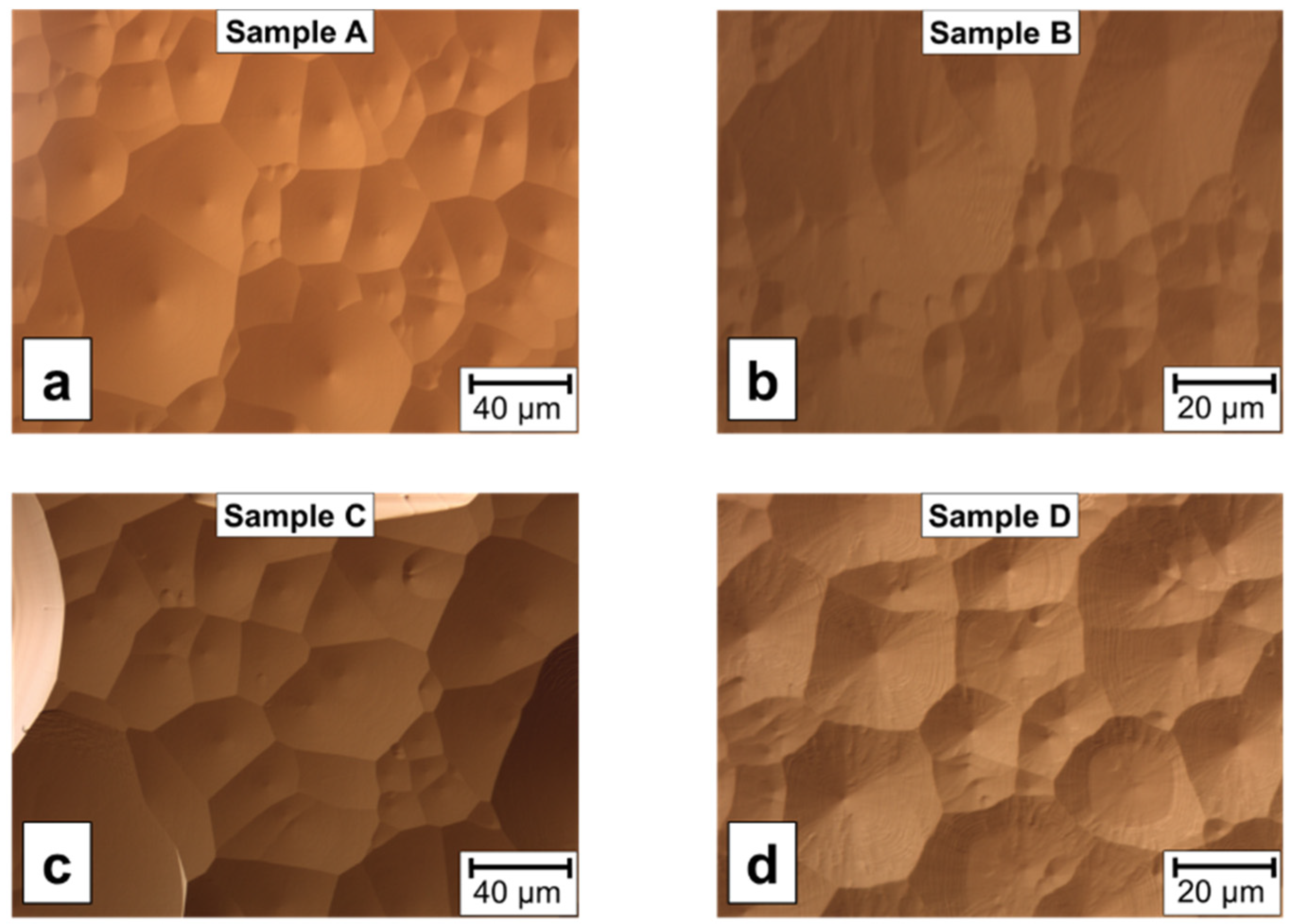
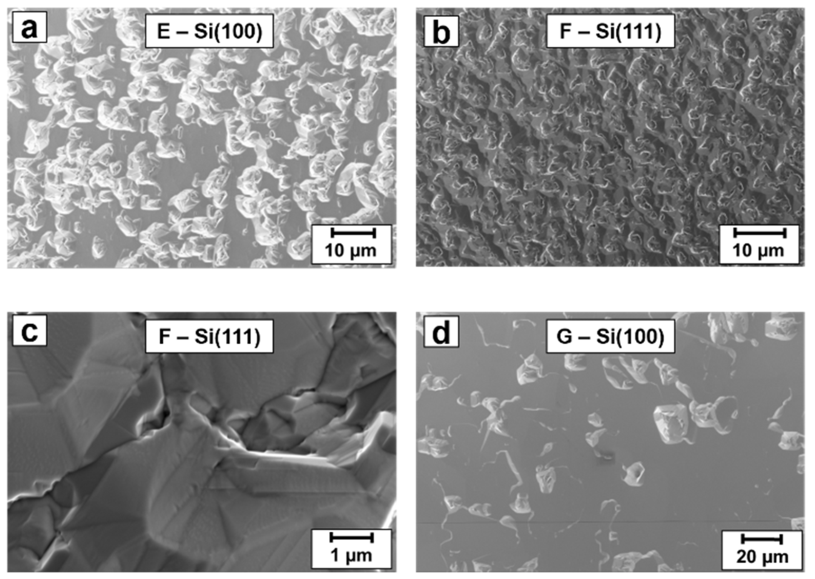
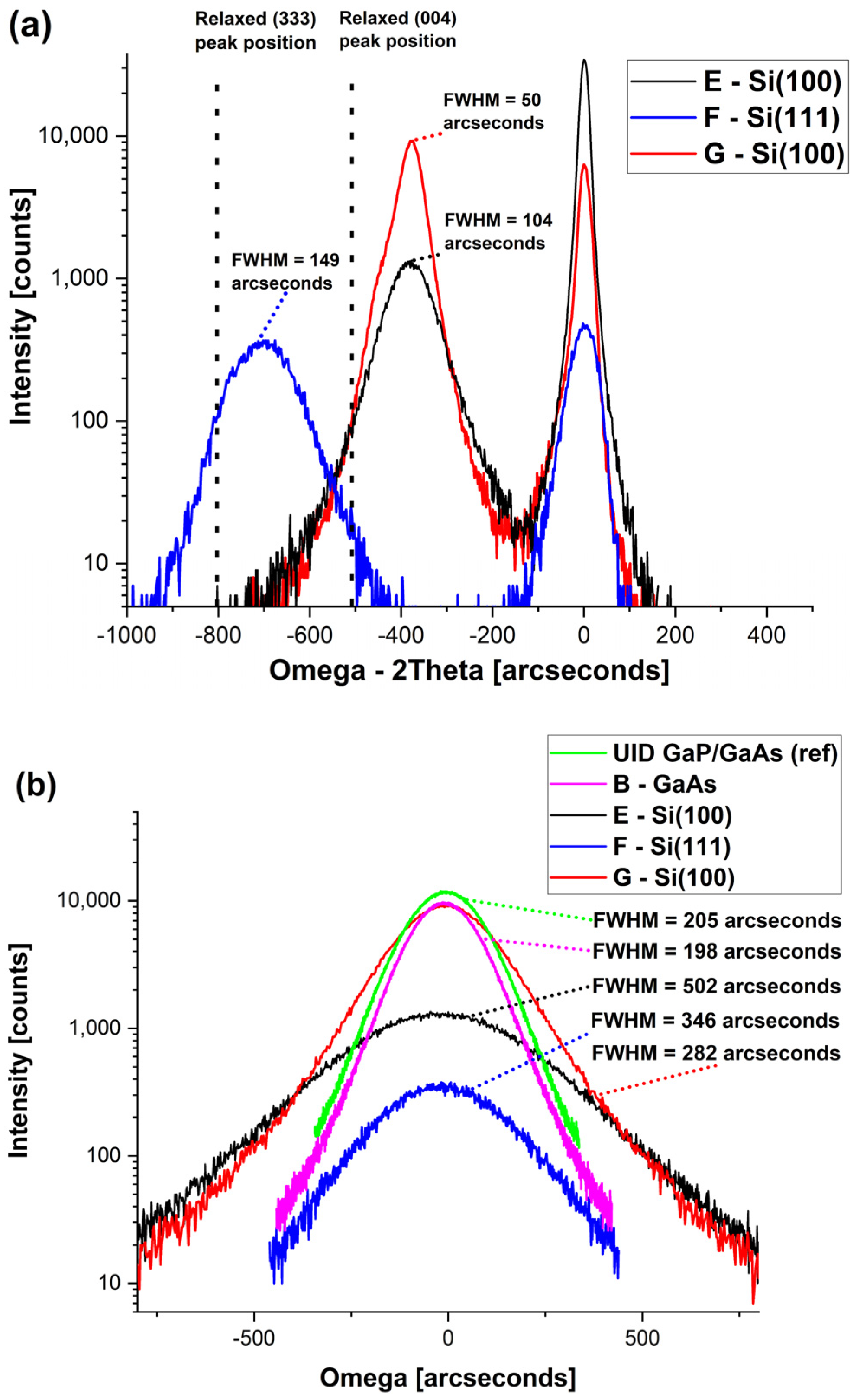
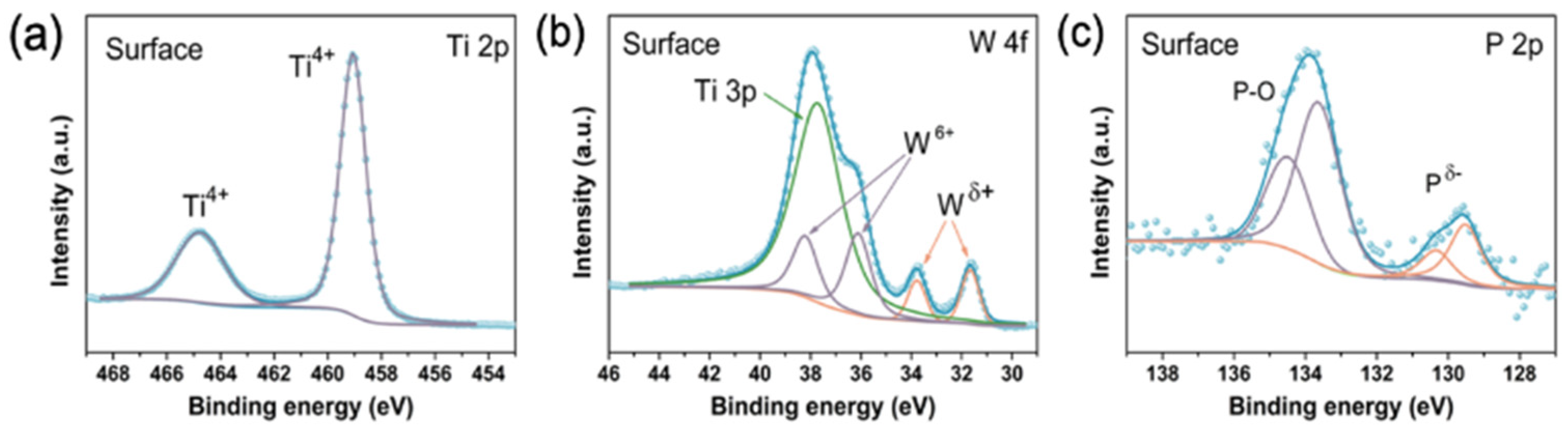
2.1. Characterisation of Heteroepitaxial p-GaP

Figure 1 shows Nomarski microscopy images showing the morphology of p-GaP/GaP and p-GaP/GaAs samples A–D. Rather than a flat, planar morphology, all samples exhibit a surface that is fully covered by hillocks. There is also no obvious difference between the homoepitaxial and heteroepitaxial samples.
The morphologies of p-GaP/Si samples E–G were characterized by scanning electron microscopy (SEM), shown in Figure 2. None of these samples as grown exhibit a flat surface, but each instead has distinct topological features. Both samples E and G grown on Si(100) have pits on the surface, whereas sample G grown with 25 sccm of GaCl exhibits significantly fewer pits than sample E grown with 5 sccm.
High-resolution X-ray diffraction (HRXRD) was used to extract crystallographic information from GaP/GaAs sample B, GaP/Si(100) samples E and G, and GaP/Si(111) sample F. Omega-2theta and omega scans, all performed using triple axis, were used to identify strain and determine the crystalline quality of the samples (Figure 3). To determine the impact of Zn-doping on GaP crystalline quality, an un-doped GaP/GaAs reference sample prepared using the same growth condition as p-GaP/GaAs sample B was included in the HRXRD omega scans. As seen by the shift in omega-2theta peak position towards the substrate (Figure 2a), all GaP/Si samples are under tensile strain likely stemming from the thermal mismatch between GaP and Si.
In terms of morphology, the heteroepitaxially grown GaP/GaAs samples B and D appear very similar to the homoepitaxial samples A and C (Figure 1). However, most likely due to the large lattice mismatch, the crystalline quality of the GaP/GaAs samples is significantly worsened; this can be seen by the relatively broad peak of the HRXRD (004) omega scan for sample B (Figure 3b). Typical FWHM values for homoepitaxial GaP is approximately 20 arcseconds, with the FWHM of GaP/GaAs sample B being a factor of 10 higher at 198 arcseconds. Assuming the broadening is only due to the randomly distributed threading dislocations (TDs) stemming from the 3.6% lattice mismatch between GaP and GaAs, this corresponds to a TD density of ~4 × 10⁷ /cm2 calculated from the Ayer’s formula [38]:
D β α   / ( 2 π × l n 2 × b 2 ) ,
where D is the dislocation density, βα is the FWHM of the omega scan, and b is the length of the Burgers vector for the threading dislocations. Additionally, as seen by the similar omega scan FWHM for p-GaP/GaAs sample B (198 arcseconds) and the un-doped reference GaP/GaAs sample (205 arcseconds), the addition of Zn-doping does not appear to significantly impact the GaP crystalline quality.
Despite the significantly lower lattice mismatch (0.36%), the samples prepared by direct heteroepitaxy of GaP on Si showed both poorer morphology (Figure 1 and Figure 2) and lower crystalline quality (Figure 3b). This is most likely caused by difficulties in achieving nucleation on Si compared to GaAs, despite using a low-temperature buffer layer. An important aspect of the epitaxy of GaP on GaAs carried out for samples B–D is the pre-heating of the GaAs substrates in PH3 before initiating the growth. This has been shown to form P-rich GaAsP islands on the GaAs surface, which is hypothesized to help relax misfit strain during the early stages of growth [39]. This effect has been reported previously by our group, where the absence of PH3 in the pre-heating ambient resulted in degraded crystalline quality of both GaAsP and GaP grown on GaAs substrates [40].
The morphology of samples E–G as seen in the SEM images (Figure 2) is much rougher than the samples grown on GaP and GaAs (Figure 1), with the GaP/Si(100) samples E and G having a high density of pits (Figure 2a,d). However, it is clear that the growth is dominated by the (001) facet for these samples, whereas for the GaP/Si(111) sample F, no single crystalline facet seems to have emerged and the morphology is characterized by a high density of randomly oriented facets (Figure 2b,c). This discrepancy in the morphology of growth on Si(100) and Si(111) substrates for samples E and F, grown under the same conditions, could be explained by the growth rate of the (100) facet compared to high-index facets. During epitaxy for which the growth rate is anisotropic, facets corresponding to crystalline orientations with low growth rate tend to emerge. If the growth rate on the (100) plane is lower compared to high-index planes, that would explain the emergence of the (100) facet for growth on the Si(100) substrates. Similarly, several high-index planes with comparable growth rates could result in the faceted morphology seen for GaP/Si(111) sample F (Figure 2b,d), if no low-index plane with low growth rate parallel to the substrate is available. This in turn would indicate that sample F is grown on (111) A plane, as this plane has a generally higher growth rate during HVPE due to the high number of dangling bonds at binding sites for Ga adatoms [41]. Another important observation is that the higher GaCl flow of 25 sccm used for GaP/Si(100) sample G improved the morphology compared to GaP/Si(100) sample E grown with 5 sccm GaCl, as seen by the lower pit density (Figure 2a,d). This can be explained by the higher GaCl flow increasing the growth rate of higher index planes to a greater extent than the (100) plane, resulting in any pits forming being effectively filled up, leaving only the (100) facet.
The pre-heating of the Si substrates in AsH3 ambient plays an important role in improving the crystalline quality for GaP/Si epitaxy. In our previous work, un-doped GaP layers were grown on Si(100) and Si(111) substrates using similar growth conditions as the ones used for samples E and F, but the substrates were pre-heated in PH3 ambient instead of AsH3 [42]. HRXRD omega scans for those samples yielded FWHM of 913 arcseconds and 419 arcseconds for GaP grown on Si(100) and Si(111), respectively. The addition of AsH3 in the pre-heating ambient decreased the FWHM to 502 arcseconds for p-GaP/Si(100) sample E and 346 arcseconds for p-GaP/Si(111) sample F in this work, implying a significant improvement in crystalline quality. This improvement can be understood by considering the Si substrate surface prior to growth. The surface energy of a pure silicon surface, both (100) and (111), is relatively high compared to Si surfaces with other terminations such as a hydrogen-terminated or oxygen-terminated surface [43,44]. For this reason, growth of III-V on Si tends to start by an initial passivation of the Si surface, either intentional or unintentional, as described in detail by Lucci et al. [45]. Furthermore, it has been shown that both a P-terminated and an As-terminated surface can be established prior to growth of GaP on Si substrates by MOVPE by using either AsH3 or PH3 pre-flow. It has also been reported that the growth of GaP on Si substrates using an AsH3 pre-flow in this manner exhibited improved crystalline quality compared to when PH3 was used [46]. This was attributed to an improved coverage of the Si surface by the Si-As monolayer compared to Si-P, resulting from the higher stability of the Si-As bond [46]. It was also attributed to a decreased GaP/Si interface energy caused by the presence of As atoms on the Si surface, leading to a shallower wetting angle which promotes layer-by-layer growth. An increased crystalline quality as a result of a greater Si surface coverage by using increased AsH3 pre-flow rate and time has been demonstrated during growth of GaAs on Si, and was attributed to a reduction in defect formation [47]. This reduction in defect density with increasing Si surface coverage was attributed to the minimization of the interface area between coalescing islands, as many defects are generated in the interfaces between islands at this stage of growth [45,47]. The shallower wetting angle reported could also lead to reduced defect density, as the smaller and more dense islands lead to misfit dislocations getting introduced to the growth after the growth coalesces. This has been proposed to lead to defects with higher mobility forming which can subsequently annihilate to a greater extent [48]. Further investigation is needed to determine the extent to which these observations also apply to growth of III-V/Si by HVPE, as the chemistry and mechanisms are quite different from MOVPE, but it is clear that the growth of GaP on both Si(100) and Si(111) benefits from heating in AsH3 ambient.
Despite the same growth conditions, the crystalline quality of GaP/Si(111) sample F is higher than GaP/Si(100) sample E as seen from the omega scan FWHM values decreasing from 502 arcseconds to 346 arcseconds (Figure 3b). Similar to the benefits from the pre-heating of Si substrates in AsH3 described above, the lower surface energy of Si(111) compared to that of Si(100) is expected to improve crystalline quality by promoting layer-by-layer growth [49]. This improvement was observed previously during VME of both GaP and GaAs on Si [40]. The crystalline quality was also improved by increasing the GaCl flow, as seen from the omega scan FWHM values for GaP/Si(100) samples E and G, reducing from 502 arcseconds to 282 arcseconds (Figure 3b). One possible explanation for this behavior is that the (100) facet could promote layer-by-layer growth to a greater extent than the higher-index facets present in the pits. We have also previously reported that an increased GaCl flow during heteroepitaxial growth of GaP on GaAs can suppress the formation of threading dislocations [40], and a similar process could take place during the heteroepitaxy of GaP on Si.

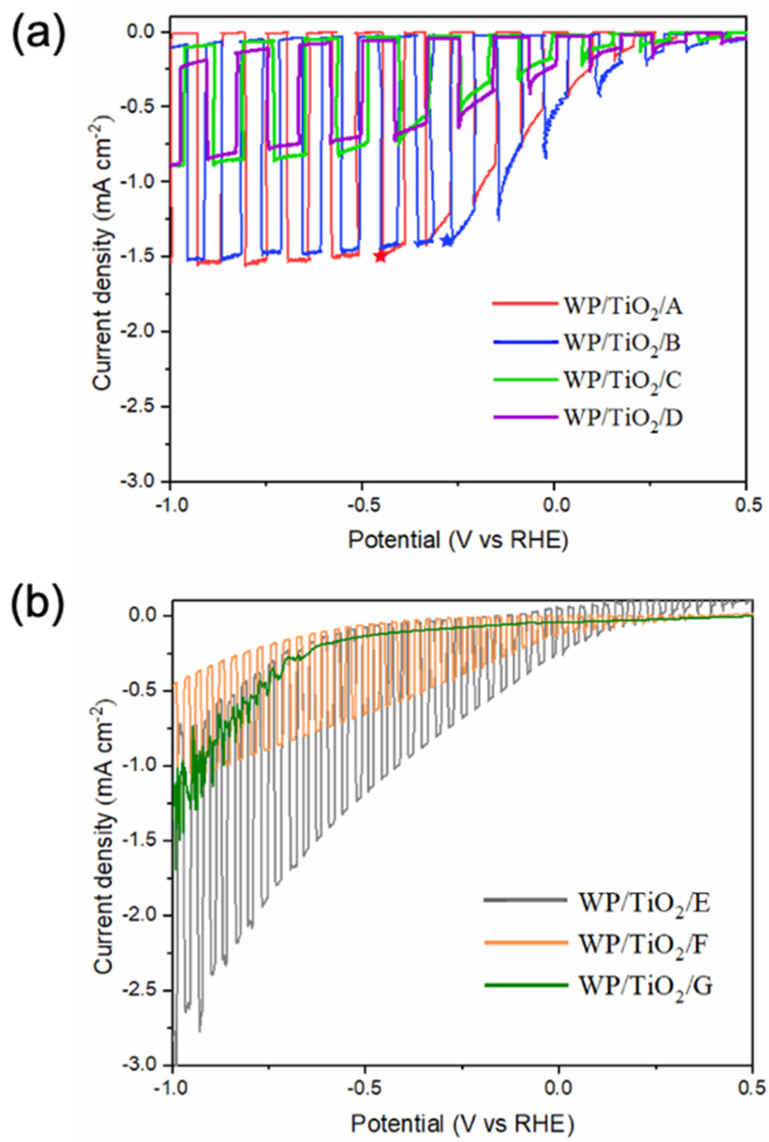
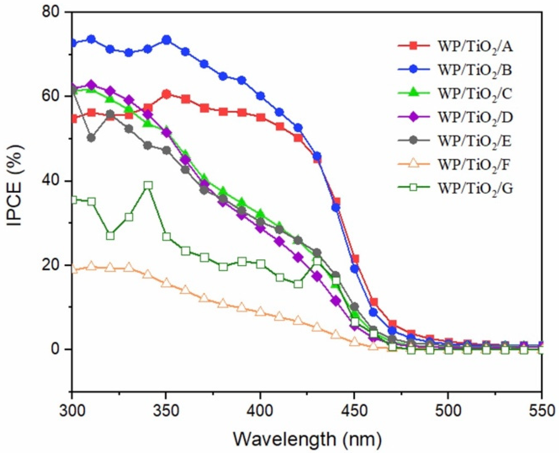
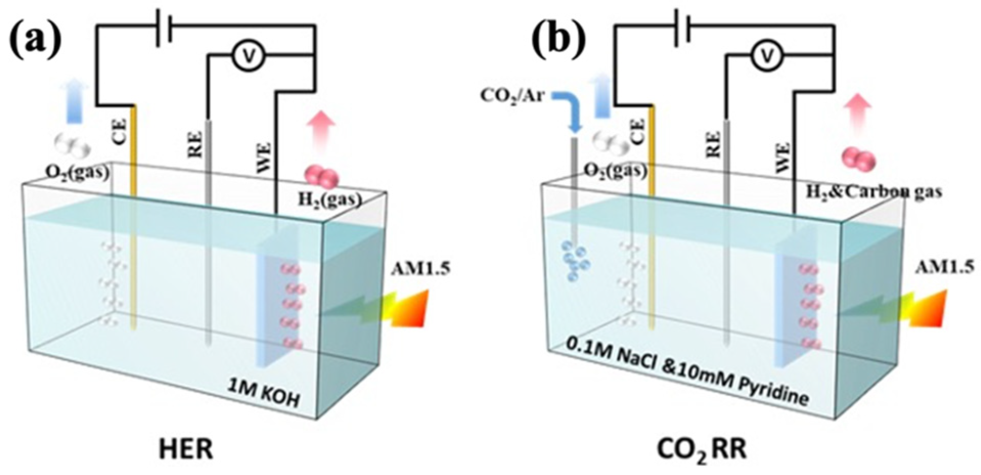
2.2. PEC Performance of WP/TiO2/p-GaP Photocathodes for Water Splitting

The chopped voltammetric curves for water splitting by WP/TiO2/p-GaP photocathode samples A–G are presented in Figure 4. As shown in Figure 4a, the homoepitaxial p-GaP/GaP sample A and heteroepitaxial p-GaP/GaAs sample B with the same Zn-doping concentration of 6.7 × 1017 cm−3 show similar saturated photocurrent density (~−1.5 mA cm−2) at −0.45 and −0.28 VRHE, respectively. Additionally, WP/TiO2/B (>0.5 VRHE) even displays a more positive onset potential compared to WP/TiO2/A (0.44 VRHE). Increasing the Zn-doping concentration from 6.7 × 1017 cm−3 in samples A and B to 8.4 × 1018 cm−3 in samples C and D resulted in an almost 50% decrease in saturated photocurrent density (~−0.8 mA cm−2). Meanwhile, high doping concentrations cause an increase in dark current density at large bias, indicating the partial breakdown of the depletion layer. Although the cation doping can narrow the band gap of GaP, the small depletion layer thickness caused by high Zn-doping concentration has a larger negative effect on the quantum efficiency.
As shown in Figure 4b, the inferior performance of the p-GaP/Si samples E–G, compared to that of samples A–B, is reasonable due to the increased defect density of these samples as indicated by the higher HRXRD omega scan FWHM values (Figure 3b). Among these three p-GaP/Si samples E–G, sample G exhibits almost no photoresponse, as seen from the chopping curve (Figure 4b). This is surprising, as it has the highest crystalline quality of the three p-GaP/Si samples. In comparison, sample E and F display higher photocurrent density despite their lower crystalline quality. This could be ascribed to the rough morphology of the samples E and F, which generally benefits HER, as it effectively increases the light absorption area and solid–liquid contact area of the photocathode. In addition to the increased surface area, a faceted surface can also increase absorption by providing a light-trapping effect [26]. Proper surface texturing could improve the PEC performance further, as has been shown by using photoelectrodes made from nanowires [50,51]. The saturated photocurrent density of sample F grown on Si (~−1.43 mA cm−2) even can be comparable with homoepitaxial sample A grown on GaP (~−1.5 mA cm−2).
To further investigate the PEC performance of these p-GaP photocathodes, IPCE measurements were performed, as shown in Figure 5. The p-GaP/GaP sample A and p-GaP/GaAs sample B exhibit excellent IPCE at the range from 300 to 420 nm and the value for sample B even exceeds 70% at near ultraviolet region. However, the IPCE of both samples A and B decreases sharply for incident light wavelengths above ~420 nm, corresponding to a photon energy equal to the GaP band gap modified by the overpotential (2.26 eV+ 0.68 eV = 2.94 eV, corresponding to 422 nm). For both p-GaP/GaP and p-GaP/GaAs samples C and D with hole concentration of 8.4 × 1018 cm−3, the IPCE is comparable to the samples with hole concentration of 6.7 × 1017 cm−3 for wavelengths of ~350 nm and below but falls off rapidly for higher wavelengths. For these samples, the use of incident photons seems to be limited primarily by other losses rather than the band gap of GaP. One such loss mechanism could be that the photons absorbed at a greater depth into the GaP photocathode generate charge-carriers that are unable to diffuse to the surface of the cathode to partake in PEC reactions. Also worth noting is that any charge carriers generated by absorption in the substrate are unlikely to reach the contacts on the surface of the p-GaP layer for this reason, and will therefore not contribute to the PEC reactions. This is most likely a result of either the reduced carrier mobility or the small depletion layer, both caused by excessive Zn-doping. The fact that the heteroepitaxial sample B with low doping outperforms the homoepitaxial sample C with high doping indicates that the doping concentration can play a more important role during PEC reactions than crystalline quality alone and needs to be carefully controlled.
As for p-GaP/Si(100) sample E, it can be seen that the IPCE at wavelengths below ~350 nm is comparable to the IPCE values for p-GaP/GaP and p-GaP/GaAs samples A–D (Figure 5). However, the IPCE for sample E drops quickly with shorter wavelengths, mimicking the behavior of the highly doped samples C and D. As the same dopant partial pressure was used for sample E as for samples A and B, this is most likely not caused by an excessive doping concentration. The overall higher defect density found in the GaP/Si samples would also reduce carrier mobility, despite the low doping. A high defect density usually results in worse PEC performance due to the reduced diffusion length caused by the increased carrier trap density [25]. Another explanation could be the formation of antiphase-domains (APDs), a common occurrence during epitaxy of III-V materials on Si substrates [52]. As APDs are charged defects, they could limit the diffusion length of carriers. This would also explain the absence of a similar sharp drop in IPCE at higher wavelengths for p-GaP/Si(111) sample F (Figure 5), as antiphase-domains do not form during growth on (111) facets.

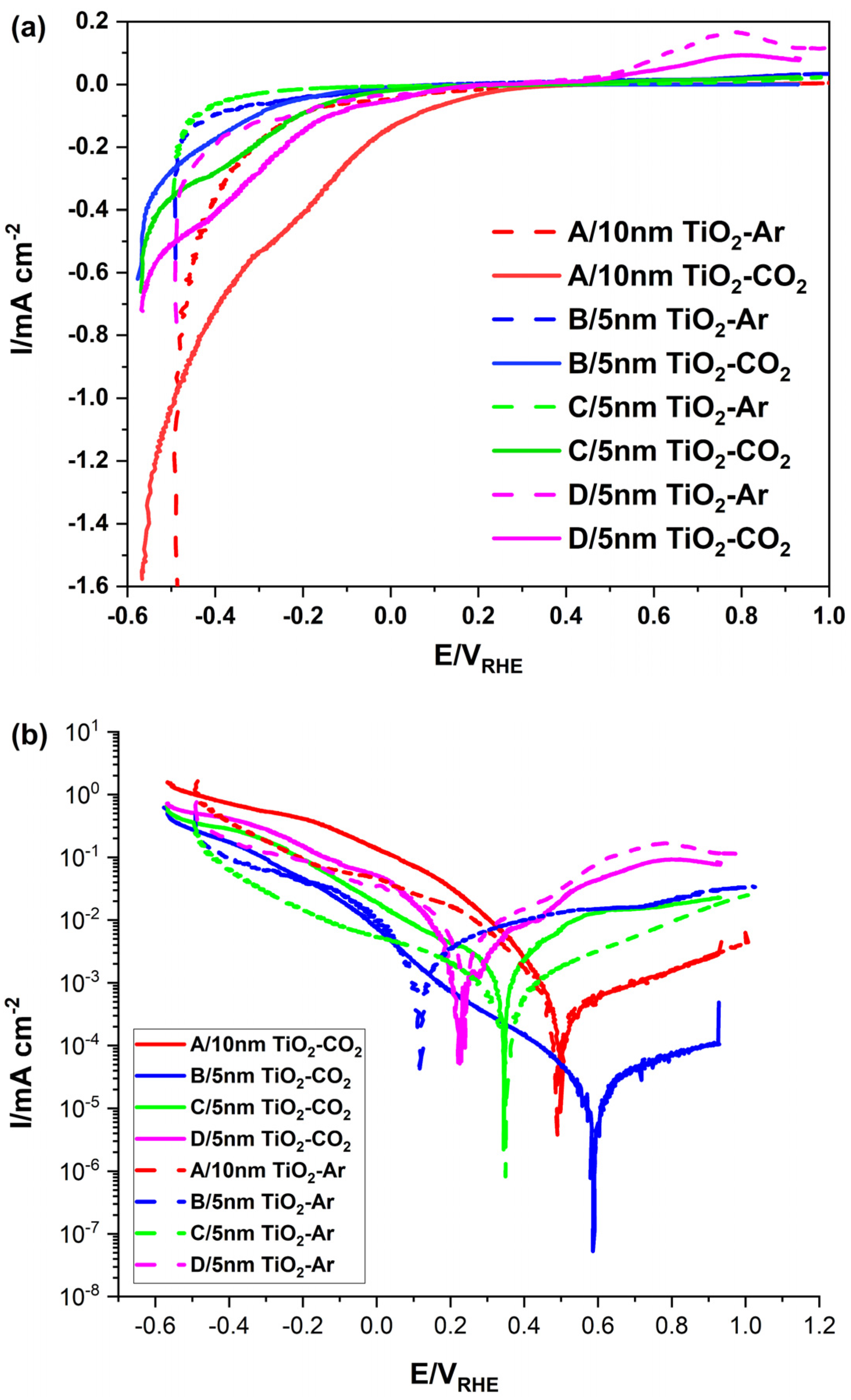
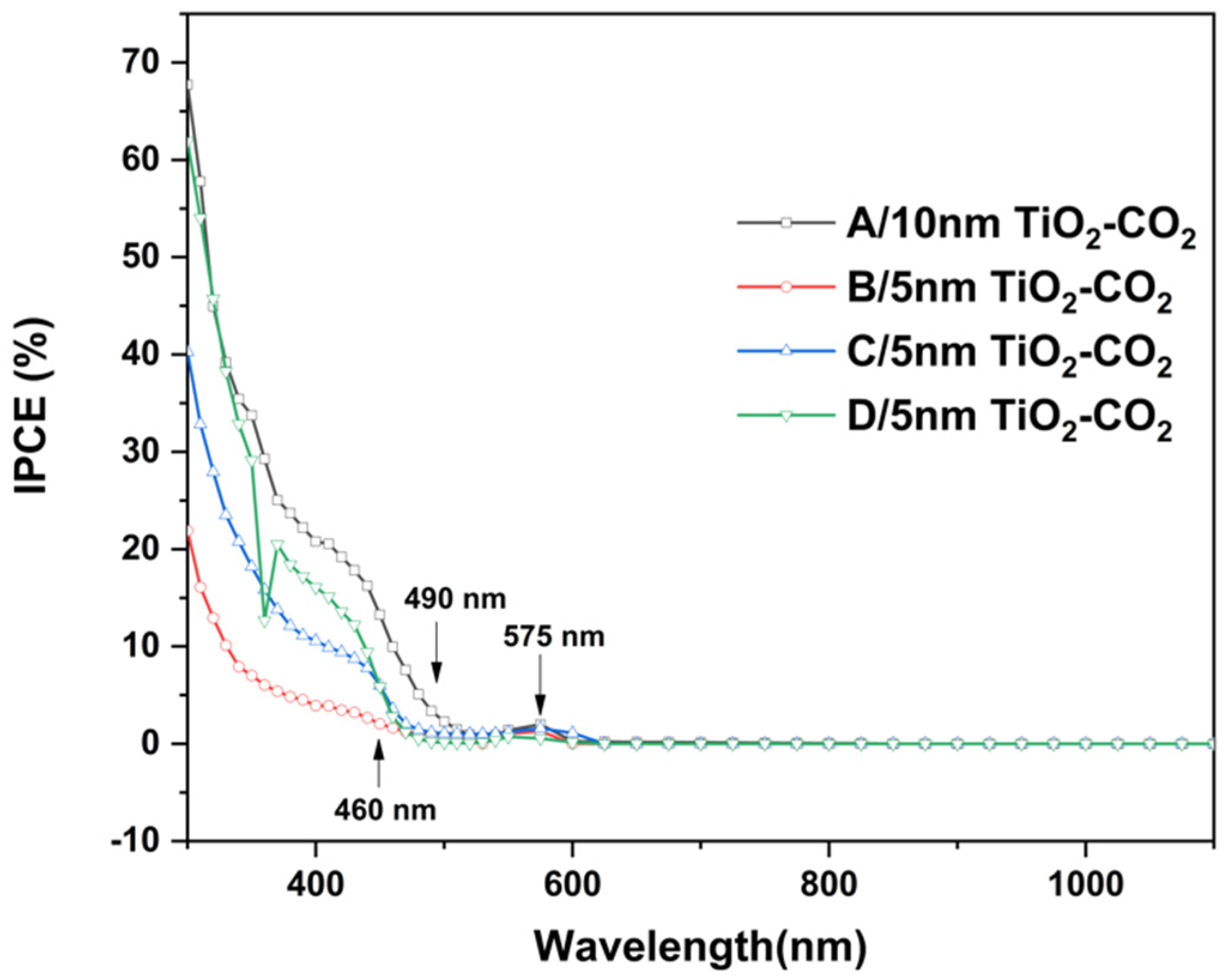
2.3. PEC Performance of TiO2/p-GaP Photocathodes for CO2 Reduction

The photocatalytic CO2 reduction behavior for p-GaP photocathodes A–D passivated with TiO2 measured in a 0.5 M NaCl and 10 mM pyridine solution saturated with Ar or CO2 under illumination are shown in Figure 6a. For the illuminated p-GaP photocathode samples, a higher photocurrent is observed in electrolyte saturated with CO2 than with Ar, indicating a catalytic reduction of CO2 [53]. The overpotentials required to drive the CO2 reduction processes with an onset of photocurrent are revealed as the voltage at minimum photocurrent in the I-V curves replotted in semi-log scale (Figure 6b). A photocathode with low onset potential is beneficial for realizing self-driven PEC reaction without external bias. The conduction bands of GaP and TiO2 are located at −0.7 and −0.2 VNHE, respectively. To reduce CO2, photoelectrons need to overcome a 1.2 V energy barrier. In theory, according to the calculation of the flat band potential, the internal pn-junction can produce nearly 0.7 V. This leads to an −0.5 V externally applied overpotential being required to drive the CO2 reduction reaction. However, the actual initial potential required is less than −0.5 V due to the reduced recombination of photogenerated carriers and the additional pn-junction photovoltage derived from the TiO2 layer. A more detailed description of the CO2RR mechanisms for TiO2/GaP photocathodes can be found in ref [17]. For p-GaP grown on GaP substrate, sample A with low doping concentration (6.76 × 10¹⁷/cm−3) has the highest photocurrent of −1.03 mA/cm2 at −0.5 VRHE and an onset potential of 0.5 VRHE in the presence of CO2 and pyridine. A lower photocurrent of −0.36 mA/cm2 at −0.5 VRHE and an onset potential of 0.34 VRHE are observed in highly doped sample C. For p-GaP heteroepitaxially grown on GaAs substrate, sample D with high hole concentration has a higher photocurrent of −0.51 mA/cm2 at −0.5 VRHE and a lower onset potential of 0.23 VRHE than sample C grown on GaP substrate. Sample B has the highest onset overpotential of 0.59 VRHE and its photocurrent is lower than that of all the other samples.
TiO2 deposited by ALD tends to have n-type doping because of oxygen vacancies [54], which creates a pn-junction in TiO2/p-GaP photocathode. It was observed that the onset overpotential could be shifted by the depletion width in pn-junction determined by the varied thickness of TiO2, and 10 nm TiO2 could be the optimum thickness, since the insulating property of thicker TiO2 will degrade its charge transfer property [17]. The high photocurrent observed in sample A could be due to thicker depletion layer in p-GaP caused by the lower doping concentration, which will increase the width of built-in electric field to enhance the efficiency of collecting photocarriers. An important aspect to consider during CO2RR is the competitive hydrogen production reaction. As shown in Figure 6a, a significantly enhanced current density in the CO2-saturated solution, compared to the Ar-saturated electrolyte, can be observed. This additional current density is generated from the direct CO2RR of the dissolved CO2 [55,56]. Since HER and CO2RR are competing reactions, the CO2 in the electrolyte will occupy the active site and inhibit hydrogen production to a certain extent. The obvious increment in reduction current can provide evidence for some CO2 reduction reaction in addition to the HER. As such, the current–potential curves provide the basis for qualitative analysis of CO2RR activity, as has been employed previously [57,58,59]. However, the specific quantitative efficiency of CO2RR is also a very important and comprehensive point to explore, and will be tested and discussed in future work.
IPCE measurements were performed for PEC CO2 reduction by p-GaP photocathodes grown on GaP and GaAs substrates, and the results are shown in Figure 7. A measurable photocurrent is observed at 575 nm for all samples, which could correspond to the photon absorption by the indirect band gap of 2.26 eV. The increase in photocurrent below 490 nm in sample A and below 460 nm in samples C and D could be related to the transition at the lowest direct band gap energy (2.8 eV). For the p-GaP photocathode grown on GaAs substrate, sample D with high hole concentration has comparable IPCE to that of sample A grown on GaP at wavelength below 350 nm.
TiO2-coated p-GaP photocathodes grown on Si were characterized with respect to PEC CO2 reduction under the same conditions, as shown in Figure 8. For samples E and F in Figure 8a, low dark currents are obtained when p-GaP photocathodes are immersed in electrolyte saturated with CO2. Under illumination, photocathodes exposed to Ar in electrolyte show an increased photocurrent density under negative bias. When photocathodes E and F are exposed to CO2 in electrolyte under illumination, a region of negative differential resistance (NDR) can be observed in I-V curves with peak photocurrent at 0.045 mA/cm2 for both samples. The mechanism of such NDR in the photocurrent of p-GaP photocathode in electrolyte saturated with CO2 is unknown. Nevertheless, a low-resistance current conduction path is created with the saturation of CO2 in electrolyte, which diminishes at high forward bias. As shown in Figure 8b, sample G has a high dark current and a low photocurrent, and breaks down when measured in electrolyte saturated with Ar or CO2, although it has a better crystalline quality with lower XRD FWHM value and smoother morphology than samples E and F.

3. Materials and Methods

3.1. Epitaxy and Material Characterisation

Zn-doped p-GaP with different doping concentrations was grown on planar GaP (100), GaAs (100), Si (100), and Si (111) substrates by low-pressure HVPE at 710 °C and 20 mbar. The growth conditions used to prepare each sample are presented in Table 1. All the growths were performed in a 5% H2 in N2 ambient using GaCl and PH3 as gallium and phosphorus precursors, respectively. The GaCl flow was varied and the PH3 flow was kept at 100 sccm. The total gas flow including the carrier gas was 900 sccm. Diethyl zinc (DEZn) was used as the precursor for p-type dopant. The p-type carrier concentration was characterized by Hall effect measurement. The DEZn flows of 10 sccm and 25 sccm result in partial pressures (p.p.) of 3.2 × 10⁻⁸ mbar and 7.5 × 10⁻⁸ mbar, respectively. These give rise to hole concentrations of 6.8 × 1017 cm−3 and 8.4 × 1018 cm−3 in GaP, respectively. The grown GaP layer thickness was ~7 µm for samples A–D and ranging from 4–16 µm for samples E–G.
Seven samples were prepared in total and divided into two groups, with 4 grown on III-V substrates and 3 grown on Si substrates. The approach for these groups is different as the growth on III-V substrates employs conventional HVPE even in the case of heteroepitaxy on GaAs. For growths on Si substrates, a variant of HVPE called VME was employed, where an undoped GaP buffer layer was grown at ~450 °C prior to the high-temperature GaP top layer growth. To facilitate the low temperature growth in HVPE the PH3 precursor was injected close to the substrate, which is necessary to reduce parasitic nucleation on the reactor wall [35]. The Si substrates were also pre-heated in AsH3 at the growth temperature in order to form an arsenic-terminated Si surface, which has been reported to enhance the growth of GaP on Si by metal–organic vapor phase epitaxy [60]. Furthermore, to reduce the threading dislocation density, a sulphur-doped GaP layer followed by an undoped GaP layer was grown before the p-GaP top layer. The GaP samples were characterized by Nomarski microscopy, scanning electron microscopy, and high-resolution X-ray diffraction.

3.2. Fabrication of p-GaP Photocathodes

All p-GaP photocathodes were prepared in the same way, regardless of the substrates used during the epitaxial growth. For CO2 reduction, amorphous TiO2 was deposited on p-GaP surface by atomic layer deposition, and mesoporous WP catalyst was additionally deposited for photocatalyzed water splitting. WP particles were omitted from the cathodes used for CO2 reduction as this would enhance the competing hydrogen evolution reaction. WP has been proven to be a great catalyst in HER; the presence of WP can not only increase the concentration of active sites but also provide a suitable hydrogen adsorption free energy for HER. In the field of CO2 reduction, Cu-based catalysts have attracted much attention, as it is the only heterogeneous catalyst to catalyze the formation of various products of hydrocarbons and oxygenates. Cu-based catalysts will be applied in future investigations into CO2 reduction. The p-GaP pieces were cleaned by ultrasonic agitation in acetone, ethanol, and deionized water before depositing the TiO2 layer by ALD. Tetrakis-dimethylamino-titanium (TDMAT, 0.1 s pulse) and water (0.015 s pulse) were used as titanium and oxygen precursors, respectively. The deposition was carried out at 150 °C for 125 cycles including a 20 s N2 purge when switching sources, which was expected to play a role in cleaning, resulting in a total TiO2 thickness of 5 nm. Highly ordered mesoporous WP was prepared with a previously reported process [37]. WP was spin-coated on the TiO2/p-GaP, followed by annealing and fixing by a necking strategy, which is described elsewhere [61]. The WP spin-coating was performed using a suspension (10 mg/mL) of WP in a 1:1 mixture of ethanol and methanol, with three 150 μL drops being separately applied to each sample at 3000 rpm. Subsequently, a 50 μL drop of TiCl4 solution in methanol (0.01 M) was applied. After spin-coating, the WP-decorated TiO2/p-GaP samples were dried at 60 °C for 10 min in air followed by annealing at 350 °C for 30 min in an Ar ambient.
The surface chemical state of the WP/TiO2 coating prepared as described above was analyzed by XPS in an earlier work, and the obtained spectra are provided in Figure 9 [62].
In the Ti 2p high-resolution spectrum (Figure 9a), the 2p3/2 and 2p1/2 of Ti4+ peaks are located at 459.1 and 464.8 eV, which is attributed to the TiO2 layer. Two states of the W atom can be observed in the W 4f spectrum (Figure 9b). The two doublets, located at 38.2, 36.1, 33.8, and 31.7 eV, belong to W6+ (W-O) and W(δ+) (W-P, 0 < δ < 4). The P 2p curves (Figure 9c) can be divided into four peaks. The pair of peaks located at 130.3 and 131.2 eV can be assigned to P-W bond while the other doublet corresponds to oxidation peaks. The high-resolution XPS spectra clearly evidence the presence of TiO2 and WP. The existence of the W-O and P-O peak indicates that strong bonds have been formed between WP mesoporous particles and TiO2 layer.
An ohmic contact was formed between p-GaP and copper wire via a eutectic gallium-indium alloy. Finally, TiO2/p-GaP and WP/TiO2/p-GaP photocathodes were encapsulated in epoxy resin before PEC measurements.

3.3. Photoelectrochemical Measurements

Photoelectrochemical hydrogen evolution reaction measurements were conducted under illumination in a three-electrode system (Figure 10a). WP/TiO2/p-GaP was used as the working electrode (WE), Hg/HgO, the reference electrode (RE) and Pt, the counter electrode (CE) in 1 M KOH solution. During chopping voltammetric testing, a 100 mW cm−2 (1 sun) simulated sunlight, which was provided by a 300 W xenon lamp (Perfect Light PLS-SXE300, China) with an air mass (AM) 1.5G filter, was incident to the front of the WP/TiO2/p-GaP. The applied potential was converted to the potential of a reversible hydrogen electrode (RHE) by Equation (1):
ERHE = EHg/HgO + 0.098 + 0.059 × pH
It is worth noting that simulating the solar spectrum using xenon lamps and AM1.5G filters can result in inaccuracies. The major discrepancy between simulated light from xenon lamps and AM1.5 global solar irradiance standard is a systematic spectral mismatch [63,64]. However, compared with other solar simulators (e.g., iodine tungsten lamp, dysprosium tungsten lamp) typically used as light sources in laboratory settings, the xenon lamp has a spectrum very close to the standard AM1.5 spectra. After optimization using an AM1.5 filter, the flux distribution is in good agreement in the visible range, although it does exhibit an inevitable cut-off in the UV and an attenuation in the near-IR. Nonetheless, as the absorbing material studied in this work is GaP, with a light absorption threshold of 550 nm, the discrepancy in the near-IR range is not expected to have a negative impact on the reliability of the measurements. Furthermore, as the UV-content of radiation reaching the earth’s surface after passing through the atmosphere as less than 7%, the discrepancy in the UV range is also not expected to have a significant impact. Therefore, the application of a xenon lamp with an AM1.5G filter can produce reliable results, as has been achieved in recently reported works [65,66].
Incident photon-to-current conversion efficiency (IPCE) of the WP/TiO2/p-GaP photocathodes were carried out at −0.68 VRHE in a quantum efficiency and IPCE measurement system (QEPVSI-b, Newport, Irvine, California, USA), and the wavelength range of monochromatic testing light was from 300 to 1100 nm.
Photoelectrochemical CO2 reduction reaction measurements were conducted under AM 1.5G irradiance in a three-electrode cell configuration with TiO2/p-GaP as the WE, Ag/AgCl as the RE and Pt as the CE (Figure 10b). An electrolyte solution with a final concentration of 0.5 M NaCl and 10 mM pyridine was used. To ensure a CO2 response, the linear sweep voltammetry (LSV) curves under Ar-saturated and CO2-saturated conditions were measured separately. Initially, argon gas was injected into the electrolyte for half an hour to ensure it was saturated. After the electrochemical test, the gas was replaced with CO2 and ventilated for half an hour before measuring the LSV curve again. The applied potential was converted to a RHE by Equation (2):
ERHE = EAg/AgCl + 0.197 + 0.059 × pH
The IPCE of the TiO2/p-GaP photocathodes for CO2RR were carried out at −0.2 VRHE in a solution with 0.5 M NaCl and 10 mM pyridine. The monochromatic light wavelength ranged from 300 to 1100 nm.

4. Conclusions

Zn-doped p-GaP was heteroepitaxially grown on GaAs and Si substrates by low-pressure HVPE using different DEZn dopant partial pressures and GaCl flows. Compared to GaP substrate, using GaAs substrates reduces the crystalline quality of GaP heteroepitaxial layer significantly but has no apparent impact on the morphology. No significant change in crystalline quality was observed from the addition of Zn-doping during heteroepitaxy of GaP on GaAs. A significant improvement in crystalline quality of GaP grown on Si by HVPE compared to our previous work, reported in [42], was achieved through the pre-heating of the Si substrates in AsH3 instead of PH3. It was also shown that the crystalline quality of GaP/Si could be improved by growing on Si(111) instead of Si(100) and by increasing the GaCl flow. For Si(100) substrates, increasing the GaCl flow also led to a smoother morphology with fewer pits. The p-GaP samples were processed to WP/TiO2/p-GaP photoelectrodes for PEC HER performance measurements. It was found that, when comparing the heteroepitaxial p-GaP/GaAs sample with the homoepitaxial p-GaP/GaP reference samples, the reduction in crystalline quality played a much smaller role in PEC HER performance than the doping concentration. It was found that excessive Zn-doping reduced the IPCE for wavelengths above 350 nm, possibly caused by the reduction in depletion layer thickness. The IPCE of p-GaP/Si sample E was comparable to that of the homoepitaxial samples at low wavelengths but showed signs of limited carrier diffusion lengths. TiO2/p-GaP photocathodes were characterized for CO2 reduction to methanol in a 0.5 M NaCl and 10 mM pyridine solution. With 10 nm TiO2 coating on p-GaP, reduced overpotential required to drive CO2 reduction process is observed. P-GaP photocathode grown on GaAs showed IPCE comparable to that grown on GaP substrate at wavelengths below 360 nm. Negative differential resistance is observed in photocatalytic current−potential curves measured on Si-based p-GaP photocathodes in electrolyte saturated with CO2 under AM1.5 illumination. The mechanism of such NDR effect requires further investigation.
The prototype GaP photoelectrodes prepared on the basis of the GaP thin films grown on the surface of GaP, GaAs and Si showed activity in photoelectrochemical hydrogen production and more specifically, CO2 reduction, under mild conditions, even though the current substrate configuration limits the full release of the potentials. Upon the improvement of crystalline quality, absorption efficiency, depletion layer thickness, and back contact, the heteroepitaxially grown p-GaP on low-cost substrates by HVPE will show significantly enhanced performance in PEC solar energy conversion.

Author Contributions

Synthesis, methodology and writing, A.S.; data curation, investigation and writing Y.Y.; formal analysis and curation, F.L.; visualization and curation, B.M.; data curation, S.L.; conceptualization and supervision, P.Z. and Y.S. All authors have read and agreed to the published version of the manuscript.

Funding

This research was funded by STINT CH2020-8716, Olle Engkvists stiftelse Nr. 200-0555 and National Natural Science Foundation of China No. 51972210 and 52111530187.

Data Availability Statement

Not applicable.

Conflicts of Interest

The authors declare no conflict of interest.

References

  1. Tyagi, H.; Agarwal, A.K.; Chakraborty, P.R.; Powar, S. Current Trends and Future Roadmap for Solar Fuels. In Advances in Solar Energy Research; Springer Nature: Singapore, 2019. [Google Scholar]
  2. Song, H.; Li, C.; Lou, Z.; Ye, Z.; Zhu, L. Effective Formation of Oxygen Vacancies in Black TiO2 Nanostructures with Efficient Solar-Driven Water Splitting. ACS Sustain. Chem. Eng. 2017, 5, 8982. [Google Scholar] [CrossRef]
  3. Zhang, R.; Ning, F.; Xu, S.; Zhou, L.; Shao, M.; Wei, M. Oxygen vacancy engineering of WO3 toward largely enhanced photoelectrochemical water splitting. Electrochim. Acta 2018, 274, 217–223. [Google Scholar] [CrossRef]
  4. Lu, Y.; Yang, Y.; Fan, X.; Li, Y.; Zhou, D.; Cai, B.; Wang, L.; Fan, K.; Zhang, K. Boosting Charge Transport in BiVO4 Photoanode for Solar Water Oxidation. Adv. Mater. 2022, 34, 2108178. [Google Scholar] [CrossRef]
  5. Gurudayal; John, R.A.; Boix, P.P.; Yi, C.; Shi, C.; Scott, M.C.; Veldhuis, S.A.; Minor, A.M.; Zakeeruddin, S.M.; Wong, L.H.; et al. Atomically Altered Hematite for Highly Efficient Perovskite Tandem Water-Splitting Devices. ChemSusChem 2017, 10, 2449. [Google Scholar] [CrossRef] [PubMed]
  6. Gurudayal; Jeong, D.; Jin, K.; Ahn, H.Y.; Boix, P.P.; Abdi, F.F.; Mathews, N.; Nam, K.T.; Wong, L.H. Highly Active MnO Catalysts Integrated onto Fe2O3 Nanorods for Efficient Water Splitting. Adv. Mater. Interfaces 2016, 3, 1600176. [Google Scholar] [CrossRef]
  7. Jiang, C.M.; Segev, G.; Hess, L.H.; Liu, G.; Zaborski, G.; Toma, F.M.; Cooper, J.K.; Sharp, I.D. Composition-Dependent Functionality of Copper Vanadate Photoanodes. ACS Appl. Mater. Interfaces 2018, 10, 10627. [Google Scholar] [CrossRef]
  8. Krol, R.V.D. Photoelectrochemical Hydrogen Production; Springer: Boston, MA, USA, 2012. [Google Scholar]
  9. Varadhan, P.; Fu, H.C.; Kao, Y.C.; Horng, R.H.; He, J.H. An efficient and stable photoelectrochemical system with 9% solar-to-hydrogen conversion efficiency via InGaP/GaAs double junction. Nat. Commun. 2019, 10, 5282. [Google Scholar] [CrossRef] [PubMed] [Green Version]
  10. Lui, Y.H.; Zhang, B.; Hu, S. Rational design of photoelectrodes for photoelectrochemical water splitting and CO2 reduction. Front. Phys. 2019, 14, 53402. [Google Scholar] [CrossRef]
  11. Deguchi, M.; Yotsuhashi, S.; Yamada, Y.; Ohkawa, K. Photoelectrochemical CO2 Conversion to Hydrocarbons Using an AlGaN/GaN-Si Tandem Photoelectrode. Adv. Condens. Matter Phys. 2015, 2015, 537860. [Google Scholar] [CrossRef] [Green Version]
  12. Zhou, X.; Liu, R.; Sun, K.; Chen, Y.; Verlage, E.; Francis, S.A.; Lewis, N.S.; Xiang, C. Solar-Driven Reduction of 1 atm of CO2 to Formate at 10% Energy-Conversion Efficiency by Use of a TiO2-Protected III–V Tandem Photoanode in Conjunction with a Bipolar Membrane and a Pd/C Cathode. ACS Energy Lett. 2016, 1, 764. [Google Scholar] [CrossRef]
  13. Canfield, D.; Frese, K.W., Jr. Reduction of Carbon Dioxide to Methanol on n - and p - GaAs and p - InP. Effect of Crystal Face, Electrolyte and Current Density. J. Electrochem. Soc. 1983, 130, 1772. [Google Scholar] [CrossRef]
  14. McCann, J.F.; Handley, L. The photoelectrochemical effect at a p-GaP electrode. Nature 1980, 283, 843. [Google Scholar] [CrossRef]
  15. Carlsson, P.; Uosaki, K.; Holmström, B.; Kita, H. Photoelectrochemical Properties of a GaP Electrode with an n/p Junction. J. Electrochem. Soc. 1989, 136, 524. [Google Scholar] [CrossRef] [Green Version]
  16. Kaiser, B.; Fertig, D.; Ziegler, J.; Klett, J.; Hoch, S.; Jaegermann, W. Solar Hydrogen Generation with Wide-Band-Gap Semiconductors: GaP(100) Photoelectrodes and Surface Modification. ChemPhysChem 2012, 13, 3053. [Google Scholar] [CrossRef] [PubMed]
  17. Zeng, G.; Qiu, J.; Li, Z.; Pavaskar, P.; Cronin, S.B. CO2 Reduction to Methanol on TiO2-Passivated GaP Photocatalysts. ACS Catal. 2014, 4, 3512. [Google Scholar] [CrossRef]
  18. Barton, E.E.; Rampulla, D.M.; Bocarsly, A.B. Selective Solar-Driven Reduction of CO2 to Methanol Using a Catalyzed p-GaP Based Photoelectrochemical Cell. J. Am. Chem. Soc. 2008, 130, 6342. [Google Scholar] [CrossRef]
  19. Walter, M.G.; Warren, E.L.; McKone, J.R.; Boettcher, S.W.; Mi, Q.; Santori, E.A.; Lewis, N.S. Solar Water Splitting Cells. Chem. Rev. 2010, 110, 6446. [Google Scholar] [CrossRef]
  20. Beyer, A.; Ohlmann, J.; Liebich, S.; Heim, H.; Witte, G.; Stolz, W.; Volz, K. GaP heteroepitaxy on Si(001): Correlation of Si-surface structure, GaP growth conditions, and Si-III/V interface structure. J. Appl. Phys. 2012, 111, 083534. [Google Scholar] [CrossRef]
  21. Grassman, T.J.; Carlin, J.A.; Galiana, B.; Yang, L.-M.; Yang, F.; Mills, M.J.; Ringel, S.A. Nucleation-related defect-free GaP/Si(100) heteroepitaxy via metal-organic chemical vapor deposition. Appl. Phys. Lett. 2013, 102, 142102. [Google Scholar] [CrossRef] [Green Version]
  22. Romanyuk, O.; Supplie, O.; Susi, T.; May, M.M.; Hannappel, T. Ab initio density functional theory study on the atomic and electronic structure of GaP/Si(001) heterointerfaces. Phys. Rev. B 2016, 94, 155309. [Google Scholar] [CrossRef]
  23. Feifel, M.; Ohlmann, J.; Benick, J.; Rachow, T.; Janz, S.; Hermle, M.; Dimroth, F.; Belz, J.; Beyer, A.; Volz, K. MOVPE Grown Gallium Phosphide–Silicon Heterojunction Solar Cells. IEEE J. Photolt. 2017, 7, 502. [Google Scholar] [CrossRef]
  24. Emmer, H.; Chen, C.T.; Saive, R.; Friedrich, D.; Horie, Y.; Arbabi, A.; Faraon, A.; Atwater, H.A. Fabrication of Single Crystal Gallium Phosphide Thin Films on Glass. Sci. Rep. 2017, 7, 4643. [Google Scholar] [CrossRef] [PubMed] [Green Version]
  25. Alqahtani, M.; Sathasivam, S.; Cui, F.; Steier, L.; Xia, X.; Blackman, C.; Kim, E.; Shin, H.; Benamara, M.; Mazur, Y.I.; et al. Heteroepitaxy of GaP on silicon for efficient and cost-effective photoelectrochemical water splitting. Mater. Chem. A 2019, 7, 8550–8558. [Google Scholar] [CrossRef]
  26. Lucci, I.; Charbonnier, S.; Vallet, M.; Turban, P.; Leger, Y.; Rohel, T.; Bertru, N.; Létoublon, A.; Rodriguez, J.B.; Cerutti, L.; et al. A Stress-Free and Textured GaP Template on Silicon for Solar Water Splitting. Adv. Fun. Mater. 2018, 28, 1801585. [Google Scholar] [CrossRef]
  27. Horowitz, K.A.W.; Remo, T.; Smith, B.; Ptak, A. A Techno-Economic Analysis and Cost Reduction Roadmap for III-V Solar Cells; National Renewable Energy Laboratory: Golden, CO, USA, 2018. Available online: https://www.nrel.gov/docs/fy19osti/72103.pdf (accessed on 10 November 2022).
  28. Simon, J.; Schulte, K.L.; Horowitz, K.A.W.; Remo, T.; Young, D.L.; Ptak, A. III-V-Based Optoelectronics with Low-Cost Dynamic Hydride Vapor Phase Epitaxy. Crystals 2019, 9, 3. [Google Scholar] [CrossRef] [Green Version]
  29. Tassev, V.L. Heteroepitaxy, an Amazing Contribution of Crystal Growth to the World of Optics and Electronics. Crystals 2017, 7, 178. [Google Scholar] [CrossRef] [Green Version]
  30. Tassev, V.; Bliss, D.; Lynch, C.; Yapp, C.; Goodhue, W.; Termoka, K. Low pressure—Temperature—Gas flow HVPE growth of GaP for nonlinear optical frequency conversion devices. J. Cryst. Growth 2010, 312, 1146. [Google Scholar] [CrossRef]
  31. Tassev, V.; Bliss, D.; Snure, M.; Bryant, G.; Peterson, R.; Bedford, R.; Yapp, C.; Goodhue, W.; Termoka, K. HVPE growth and characterization of gap on different substrates and patterned templates for frequency conversion devices. J. Eur. Opt. Soc. Rap. Public 2011, 6, 11017. [Google Scholar] [CrossRef] [Green Version]
  32. Vangala, S.; Kimani, M.; Peterson, R.; Stites, R.; Snure, M.; Tassev, V. Thick orientation-patterned growth of GaP on wafer-fused GaAs templates by hydride vapor phase epitaxy for frequency conversion. Opt. Mater. 2016, 60, 62. [Google Scholar] [CrossRef]
  33. Tassev, V.L.; Vangala, S.R. Thick Hydride Vapor Phase Heteroepitaxy: A Novel Approach to Growth of Nonlinear Optical Materials. Crystals 2019, 9, 393. [Google Scholar] [CrossRef]
  34. Schunemann, P.G.; Johnson, K.; Farrell, C.; Maidment, L.; Shi, Y.; Rutkauskas, M.; Reid, D.T. Continuous wavelength tuning from 3.9–12 µm from an optical parametric oscillator based on orientation-patterned GaP grown on GaAs. Opt. Mater. Exp. 2021, 11, 654. [Google Scholar] [CrossRef]
  35. Mori, H.; Ogasawara, M.; Yamamoto, M.; Tachikawa, M. New hydride vapor phase epitaxy for GaP growth on Si. Appl. Phys. Lett. 1987, 51, 1245. [Google Scholar] [CrossRef]
  36. Mori, H.; Tachikawa, M.; Sugo, M.; Itoh, Y. GaAs heteroepitaxy on an epitaxial Si surface with a low-temperature process. Appl. Phys. Lett. 1993, 63, 1963. [Google Scholar] [CrossRef]
  37. Li, F.; Wang, C.; Han, X.; Feng, X.; Qu, Y.; Liu, J.; Chen, W.; Zhao, L.; Song, X.; Zhu, H.; et al. Confinement Effect of Mesopores: In Situ Synthesis of Cationic Tungsten-Vacancies for a Highly Ordered Mesoporous Tungsten Phosphide Electrocatalyst. ACS Appl. Mater. Interfaces 2020, 12, 22741–22750. [Google Scholar] [CrossRef]
  38. Ayers, J.E. The measurement of threading dislocation densities in semiconductor crystals by X-ray diffraction. J. Cryst. Growth 1994, 135, 71. [Google Scholar] [CrossRef]
  39. Tassev, V.L.; Vangala, S.R.; Peterson, R.D.; Snure, M.J. Heteroepitaxy of orientation-patterned nonlinear optical materials. J. Cryst. Growth 2018, 486, 155. [Google Scholar] [CrossRef]
  40. Strömberg, A.; Omanakuttan, G.; Liu, Y.; Mu, T.; Xu, Z.; Lourdudoss, S.; Sun, Y. Heteroepitaxy of GaAsP and GaP on GaAs and Si by low pressure hydride vapor phase epitaxy. J. Cryst. Growth 2020, 540, 125623. [Google Scholar] [CrossRef]
  41. Lafon, E.G.; Napierala, J.; Castelluci, D.; Pimpinelli, A.; Cadoret, R.; Gérard, B. Selective growth of GaAs by HVPE: Keys for accurate control of the growth morphologies. J. Cryst. Growth 2001, 222, 482. [Google Scholar] [CrossRef]
  42. Strömberg, A.; Bhargava, P.; Xu, Z.; Lourdudoss, S.; Sun, Y. Direct Heteroepitaxy and Selective Area Growth of GaP and GaAs on Si by Hydride Vapor Phase Epitaxy. Phys. Status Solidi A 2021, 218, 2000447. [Google Scholar] [CrossRef]
  43. Northrup, J.E. Structure of Si(100)H: Dependence on the H chemical potential. Phys. Rev. B 1991, 44, 1419. [Google Scholar] [CrossRef]
  44. Widjaja, Y.; Musgrave, C.B. Atomistic mechanism of the initial oxidation of the clean Si(100)-(2 × 1) surface by O2 and SiO2 decomposition. J. Chem. Phys. 2002, 116, 5774. [Google Scholar] [CrossRef]
  45. Lucci, I.; Charbonnier, S.; Pedesseau, L.; Vallet, M.; Cerutti, L.; Rodriguez, J.-B.; Tournié, E.; Bernard, R.; Létoublon, A.; Bertru, N.; et al. Universal description of III-V/Si epitaxial growth processes. Phys. Rev. Mater. 2018, 2, 060401. [Google Scholar] [CrossRef] [Green Version]
  46. Kohama, Y.; Uchida, K.; Soga, T.; Jimbo, T.; Umeno, M. Quality improvement of metalorganic chemical vapor deposition grown GaP on Si by AsH3 preflow. Appl. Phys. Lett. 1988, 53, 862. [Google Scholar] [CrossRef]
  47. Asai, K.; Fujita, K.F.K.; Shiba, Y.S.Y. The Effects of AsH3 Preflow Conditions at Low Temperature on the Morphology of GaAs Buffer Layers for GaAs/Si Grown by Metalorganic Chemical Vapor Deposition. Jpn. J. Appl. Phys. 1991, 30, L1967. [Google Scholar] [CrossRef]
  48. Bolkhovityanov, Y.B.; Pchelyakov, O.P. GaAs epitaxy on Si substrates: Modern status of research and engineering. Phys. Usp. 2008, 51, 437. [Google Scholar] [CrossRef]
  49. Xu, H.Y.; Guo, Y.N.; Wang, Y.; Zou, J.; Kang, J.H.; Gao, Q.; Tan, H.H.; Jagadish, C. Effects of annealing and substrate orientation on epitaxial growth of GaAs on Si. J. Appl. Phys. 2009, 106, 083514. [Google Scholar] [CrossRef] [Green Version]
  50. Xie, G.; Jana, S.U.; Dong, Z.; Dai, Y.; Boddula, R.; Wei, Y.; Zhao, C.; Xin, Q.; Wang, J.-N.; Du, Y.; et al. GaP/GaPN core/shell nanowire array on silicon for enhanced photoelectrochemical hydrogen production. Chin. J. Catal. 2020, 41, 2. [Google Scholar] [CrossRef]
  51. Abbas, Y.; Zuhra, Z.; Akhtar, N.; Ali, S.; Gong, J.R. Single-Step Fabrication of Visible-Light-Active ZnO-GaN:ZnO Branched Nanowire Array Photoanodes for Efficient Water Splitting. ACS Appl. Energy Mater. 2018, 1, 3529. [Google Scholar] [CrossRef]
  52. Krost, A.; Schnabel, R.F.; Heinrichsdorff, F.; Rossow, U.; Bimberg, D.; Cerva, H. Defect reduction in GaAs and InP grown on planar Si(111) and on patterned Si(001) substrates. J. Cryst. Growth 1994, 145, 314–320. [Google Scholar] [CrossRef]
  53. Seshadri, G.; Lin, C.; Bocarsly, A.B. A new homogeneous electrocatalyst for the reduction of carbon dioxide to methanol at low overpotential. J. Electroanal. Chem. 1994, 372, 145. [Google Scholar] [CrossRef]
  54. Morgan, B.J.; Watson, G.W. Intrinsic n-type Defect Formation in TiO2: A Comparison of Rutile and Anatase from GGA+U Calculations. J. Phys. Chem. C 2010, 114, 2321. [Google Scholar] [CrossRef]
  55. Xu, H.; Rebollar, D.; He, H.; Chong, L.; Liu, Y.; Liu, C.; Sun, C.-J.; Li, T.; Muntean, J.V.; Winans, R.E.; et al. Highly selective electrocatalytic CO2 reduction to ethanol by metallic clusters dynamically formed from atomically dispersed copper. Nat. Energy 2020, 5, 623–632. [Google Scholar] [CrossRef]
  56. Wu, J.; Yadav, R.M.; Liu, M.; Sharma, P.P.; Tiwary, C.S.; Ma, L.; Zou, X.; Zhou, X.-D.; Yakobson, B.I.; Lou, J.; et al. Achieving Highly Efficient, Selective, and Stable CO2 Reduction on Nitrogen-Doped Carbon Nanotubes. ACS Nano 2015, 9, 5364–5371. [Google Scholar] [CrossRef] [PubMed]
  57. Lim, Y.J.; Seo, D.; Abbas, S.A.; Jung, H.; Ma, A.; Lee, K.; Lee, G.; Lee, H.; Nam, K.M. Unraveling the Simultaneous Enhancement of Selectivity and Durability on Single-Crystalline Gold Particles for Electrochemical CO2 Reduction. Adv. Sci. 2022, 9, 2201491. [Google Scholar] [CrossRef]
  58. Nguyen, D.L.T.; Jee, M.S.; Won, D.H.; Jung, H.; Oh, H.-S.; Min, B.K.; Hwang, Y.J. Selective CO2 Reduction on Zinc Electrocatalyst: The Effect of Zinc Oxidation State Induced by Pretreatment Environment. ACS Sustain. Chem. Eng. 2017, 5, 11377–11386. [Google Scholar] [CrossRef]
  59. Qi, K.; Zhang, Y.; Li, J.; Charmette, C.; Ramonda, M.; Cui, X.; Wang, Y.; Zhang, Y.; Wu, H.; Wang, W.; et al. Enhancing the CO2-to-CO Conversion from 2D Silver Nanoprisms via Superstructure Assembly. ACS Nano 2021, 15, 7682–7693. [Google Scholar] [CrossRef]
  60. Kohama, Y.; Kadota, Y.; Ohmachi, Y. Initial Stages of Epitaxial Growth of GaP on Si with AsH3 Preflow. Jpn. J. Appl. Phys. 1990, 29, L229. [Google Scholar] [CrossRef]
  61. Li, F.; Zheng, W.; Liu, J.; Zhao, L.; Janackovic, D.; Qiu, Y.; Song, X.; Zhang, P.; Gao, L. Enhancing the Long-Term Photoelectrochemical Performance of TiO2/Si Photocathodes by Coating of Ti-Doped Mesoporous Hematite. ACS Appl. Energy Mater. 2021, 4, 7882–7890. [Google Scholar] [CrossRef]
  62. Li, F.; Yuan, Y.; Feng, X.; Liu, J.; Chen, S.; Lin, Y.; Sun, Y.; Chen, H.; Zhao, L.; Song, X.; et al. Coating of Phosphide Catalysts on p-Silicon by a Necking Strategy for Improved Photoelectrochemical Characteristics in Alkaline Media. ACS Appl. Mater. Interfaces 2021, 13, 20185–20193. [Google Scholar] [CrossRef]
  63. Döscher, H.; Young, J.L.; Geisz, J.F.; Turner, J.A.; Deutsch, T.G. Solar-to-hydrogen efficiency: Shining light on photoelectrochemical device performance. Energy Environ. Sci. 2016, 9, 74. [Google Scholar] [CrossRef]
  64. Wang, Y.; Liu, X.; Zhou, Z.; Ru, P.; Chen, H.; Yang, X.; Han, L. Reliable Measurement of Perovskite Solar Cells. Adv. Mater. 2019, 31, 1803231. [Google Scholar] [CrossRef] [PubMed]
  65. Li, Y.; Wu, Q.; Chen, Y.; Zhang, R.; Li, C.; Zhang, K.; Li, M.; Lin, Y.; Wang, D.; Zou, X.; et al. Interface engineering Z-scheme Ti-Fe2O3/In2O3 photoanode for highly efficient photoelectrochemical water splitting. Appl. Catal. B Environ. 2021, 290, 120058. [Google Scholar] [CrossRef]
  66. Ning, X.; Wu, Q.; Fan, Y.; Zhang, Q.; Du, P.; Zhang, D.; Chen, J.; Lu, X. Plasmon-Enhanced Charge Separation and Surface Reactions Based on Ag-Loaded Transition-Metal Hydroxide for Photoelectrochemical Water Oxidation. Adv. Energy Mater. 2021, 11, 2100405. [Google Scholar] [CrossRef]
Figure 1. Nomarski microscopy images of surface morphology for (a) sample A, (b) sample B, (c) sample C, and (d) sample D.
Catalysts 12 01482 g001
Figure 2. SEM images showing (a) GaP/Si(100) sample E; (b) GaP/Si(111) sample F; (c) close-up of sample F shown in (b); (d) GaP/Si(100) sample G.
Catalysts 12 01482 g002
Figure 3. (a) HRXRD omega-2theta scans of samples E–G, indicating the position of the relaxed (004) and (333) GaP peaks. The FWHM values for the layer peaks of samples E-G are also indicated. The (004) peak was scanned for samples E and G, and the (333) peak was scanned for sample F. (b) HRXRD GaP-peak omega scans of sample B and E–F, indicating the FWHM for each. The (004) peak was scanned for sample B, E, and G, and the (333) peak was scanned for sample F.
Catalysts 12 01482 g003
Figure 4. Chopping I-V curves measured on samples A–D (a) and E–G (b) with WP/TiO2 coatings on p-GaP surface in 1M KOH electrolyte. Potential is replotted with respect to reversible hydrogen electrode (RHE).
Catalysts 12 01482 g004
Figure 5. IPCE curves measured at −0.68 VRHE on samples A–G with WP/TiO2 coatings on p-GaP surface in 1M KOH electrolyte.
Catalysts 12 01482 g005
Figure 6. Photocatalytic current−potential curves of p-GaP photocathodes with TiO2 in a 0.5 M NaCl and 10 mM pyridine solution saturated with Ar or CO2 measured under AM1.5 irradiance and plotted in (a) linear and (b) semi-log scale. Potential replotted with respect to reference hydrogen electrode (RHE). Onset potentials of p-GaP photocathodes are revealed in (b).
Catalysts 12 01482 g006
Figure 7. IPCE curves of PEC CO2 reduction measured at −0.2 VRHE on samples A–D with TiO2 coating on p-GaP surface in 0.5 M NaCl and 10 mM pyridine solution saturated with CO2.
Catalysts 12 01482 g007
Figure 8. Photocatalytic current−potential curves of TiO2-coated p-GaP/Si photocathode samples (a) E, F and (b) G in 0.5 M NaCl and 10 mM pyridine solution saturated with Ar or CO2 measured under AM1.5 irradiance and in the dark. Potential replotted with respect to reversible hydrogen electrode (RHE).
Catalysts 12 01482 g008
Figure 9. XPS survey of WP/TiO2 on a Si surface. (a) Ti 2p spectrum, (b) W 4f spectrum and (c) P 2p spectrum from the surface of WP/TiO2. Reprinted/adapted with permission from Ref. [62]. 2021, ACS Publications.
Catalysts 12 01482 g009
Figure 10. Three-electrode configurations used for photoelectrochemical (a) hydrogen evolution reaction (HER) and (b) CO2 reduction reaction (CO2RR) measurements. CE: counter electrode; RE: reference electrode; WE: work electrode.
Catalysts 12 01482 g010
Table 1. Summary of p-GaP growth conditions.
SampleSubstrateDEZn Flow
[sccm]
GaCl Flow
[sccm]
PH3
[sccm]
AGaP105100
BGaAs105100
CGaP255100
DGaAs255100
ESi (100)105100
FSi (111)105100
GSi (100)1025100
Publisher’s Note: MDPI stays neutral with regard to jurisdictional claims in published maps and institutional affiliations.

