

Fabrication of Carbon/Zinc Oxide Nanocomposites as Highly Efficient Catalytic Materials for Application in Dye-Sensitized Solar Cells
 , ,
, ,
Abstract
:
1. Introduction
2. Results and Discussion
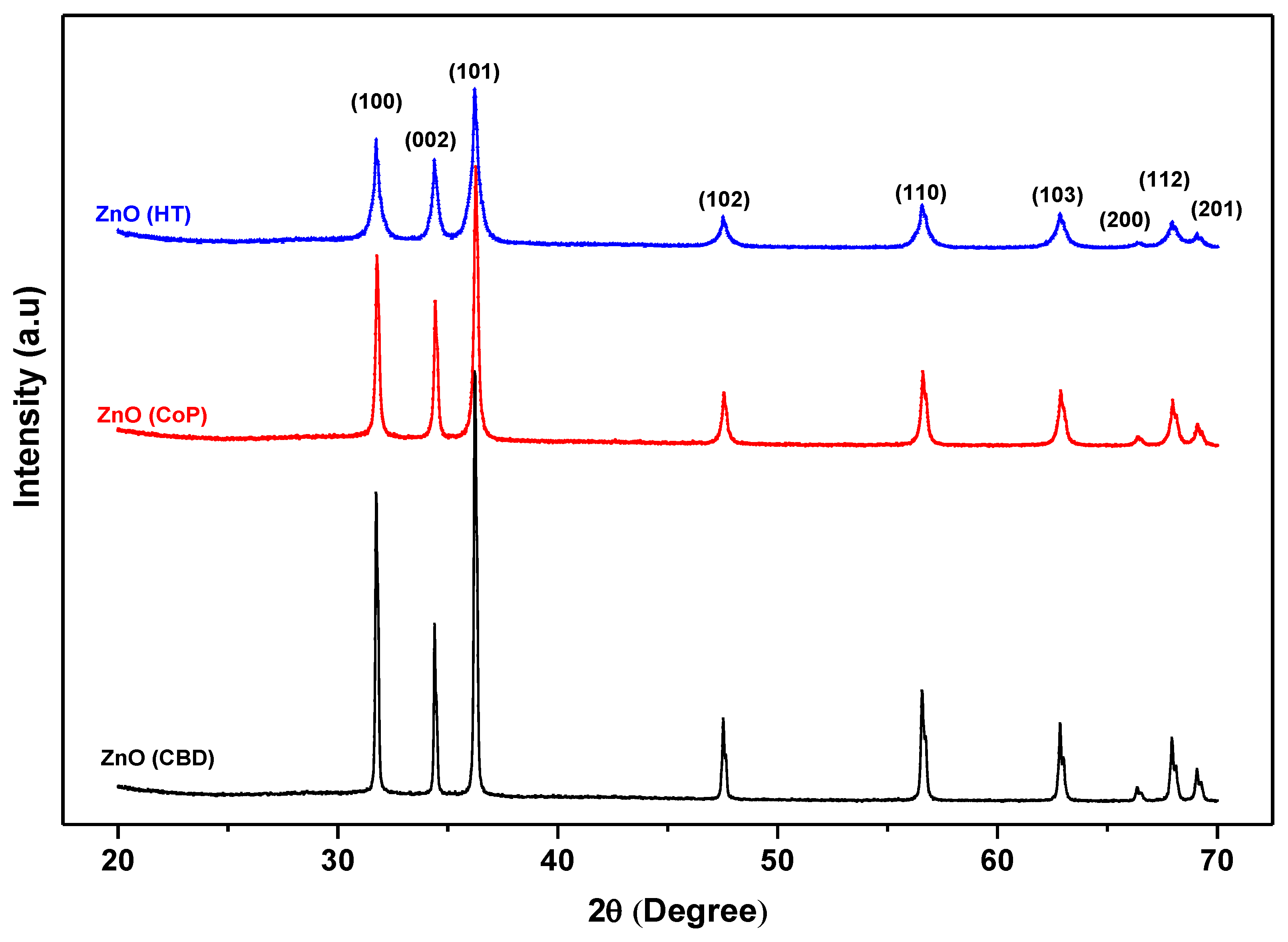
2.1. X-ray Diffraction (XRD) Analysis
2.1.1. XRD Analysis of ZnO Nanostructures
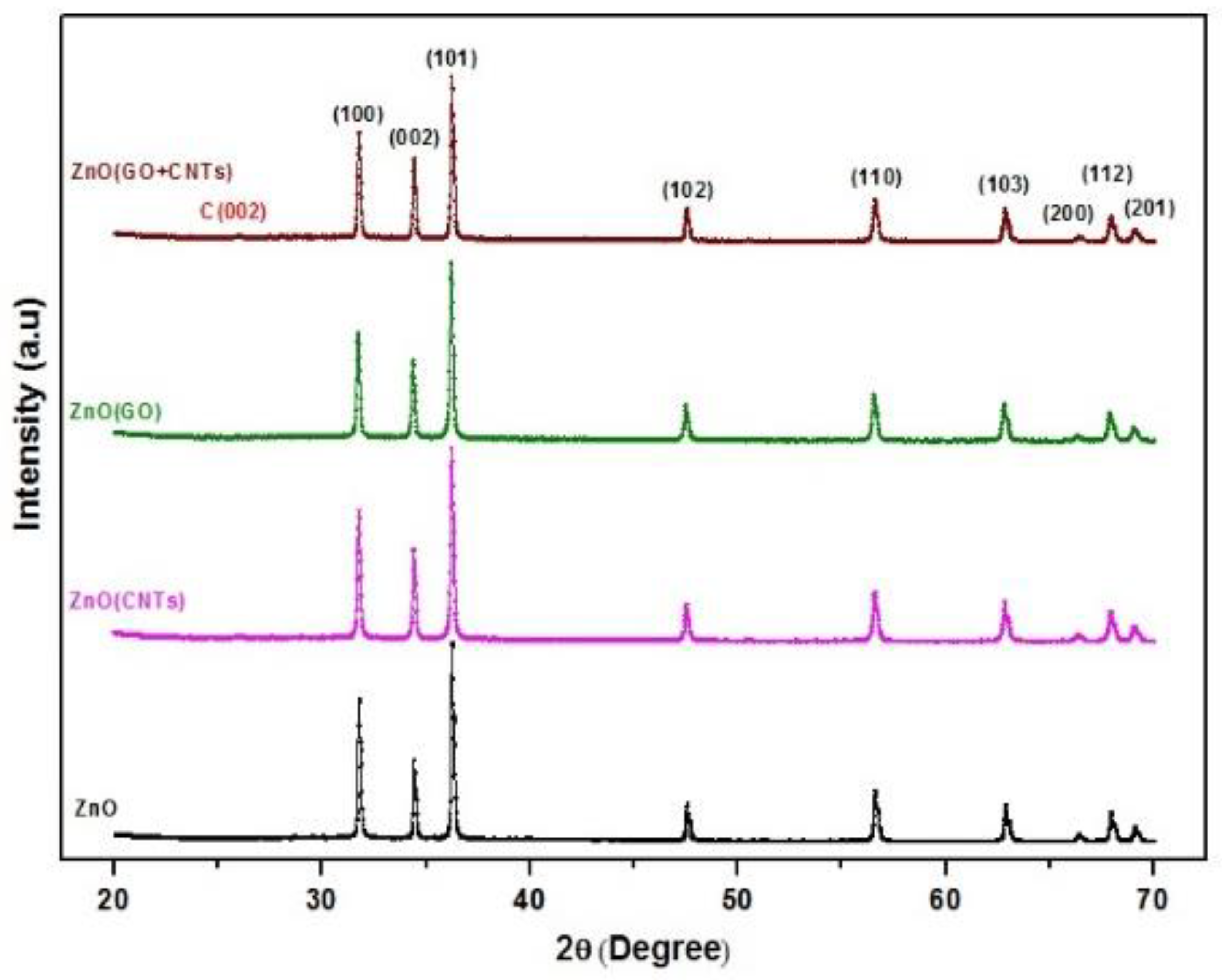
2.1.2. XRD Analysis of ZnO/CNTs/GO Nanocomposites
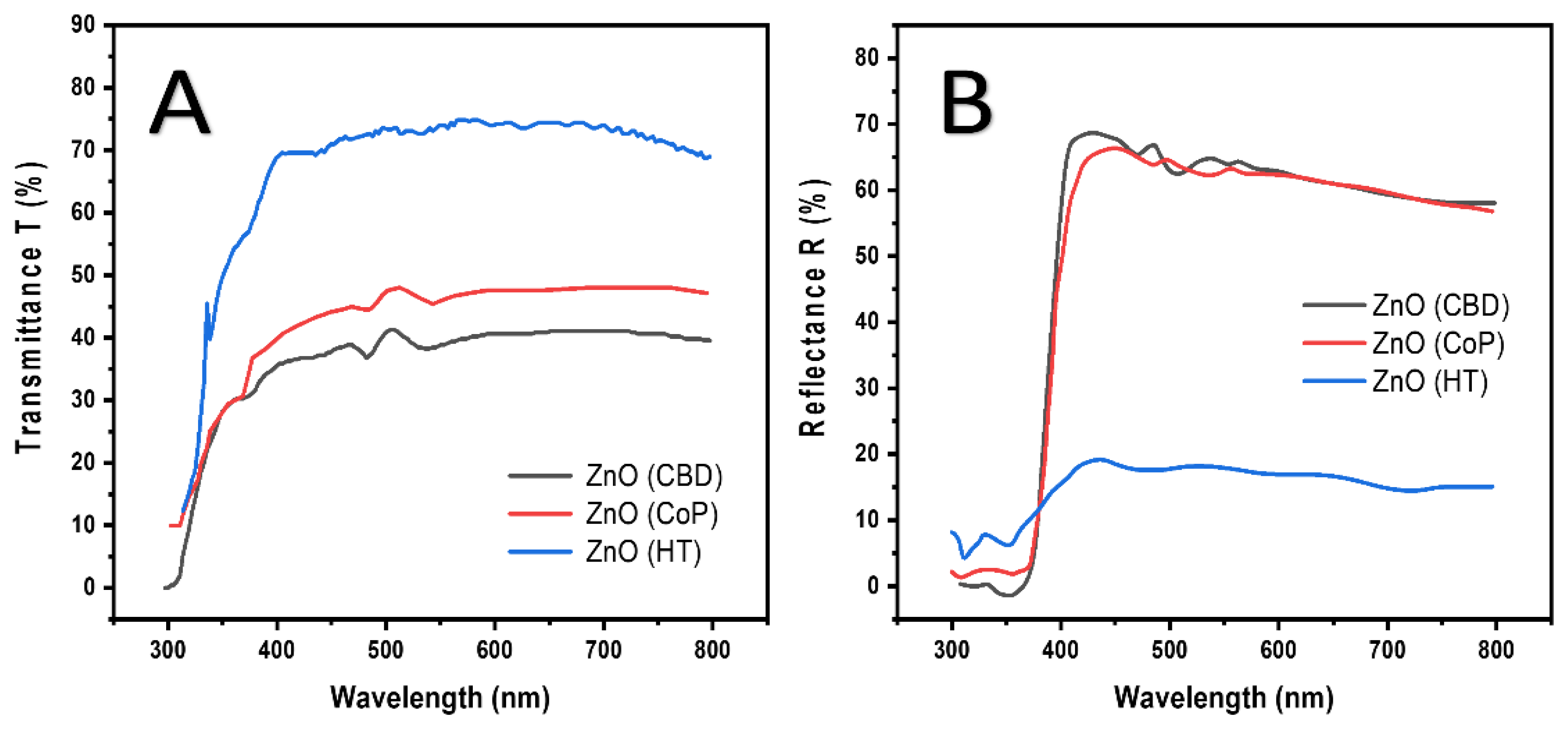
2.2. Optical Analysis
2.2.1. Optical Analysis of ZnO Nanostructures
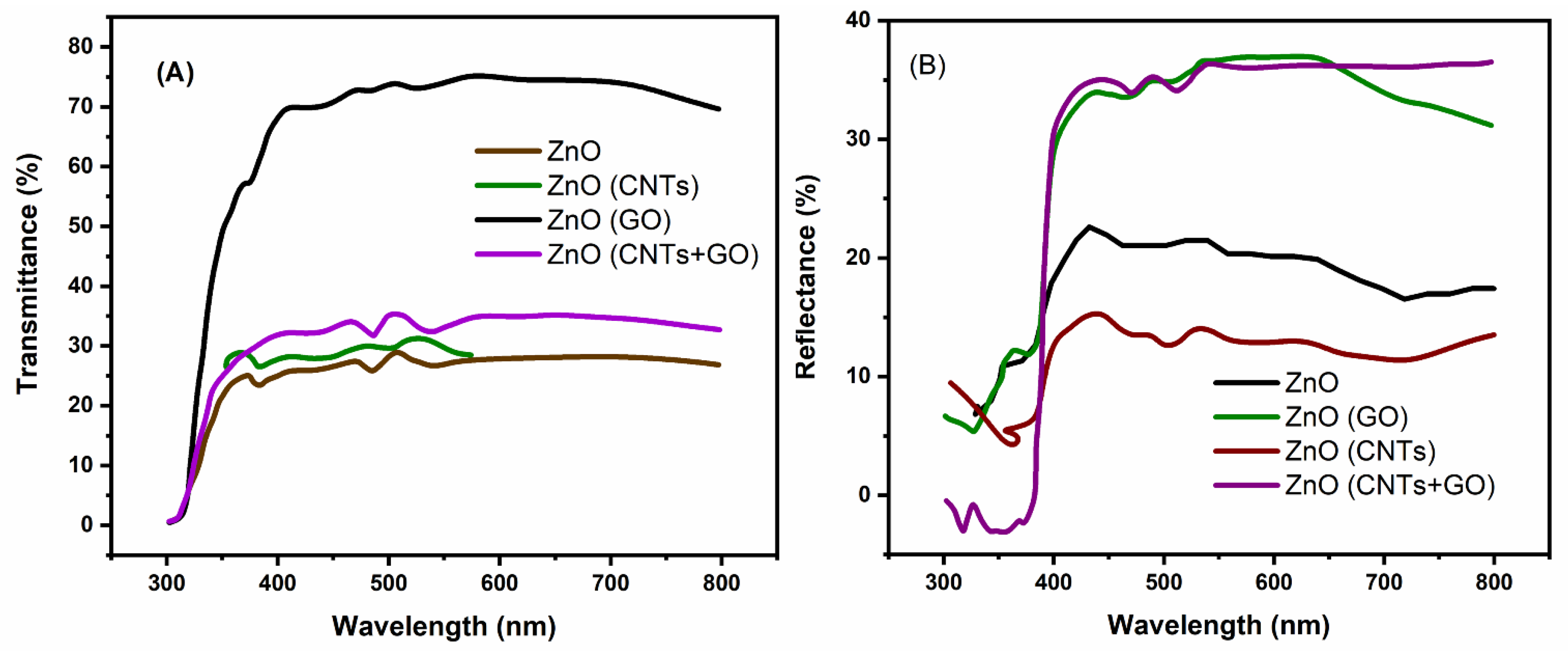
2.2.2. Optical Analysis of ZnO/CNTs/GO Nanocomposites
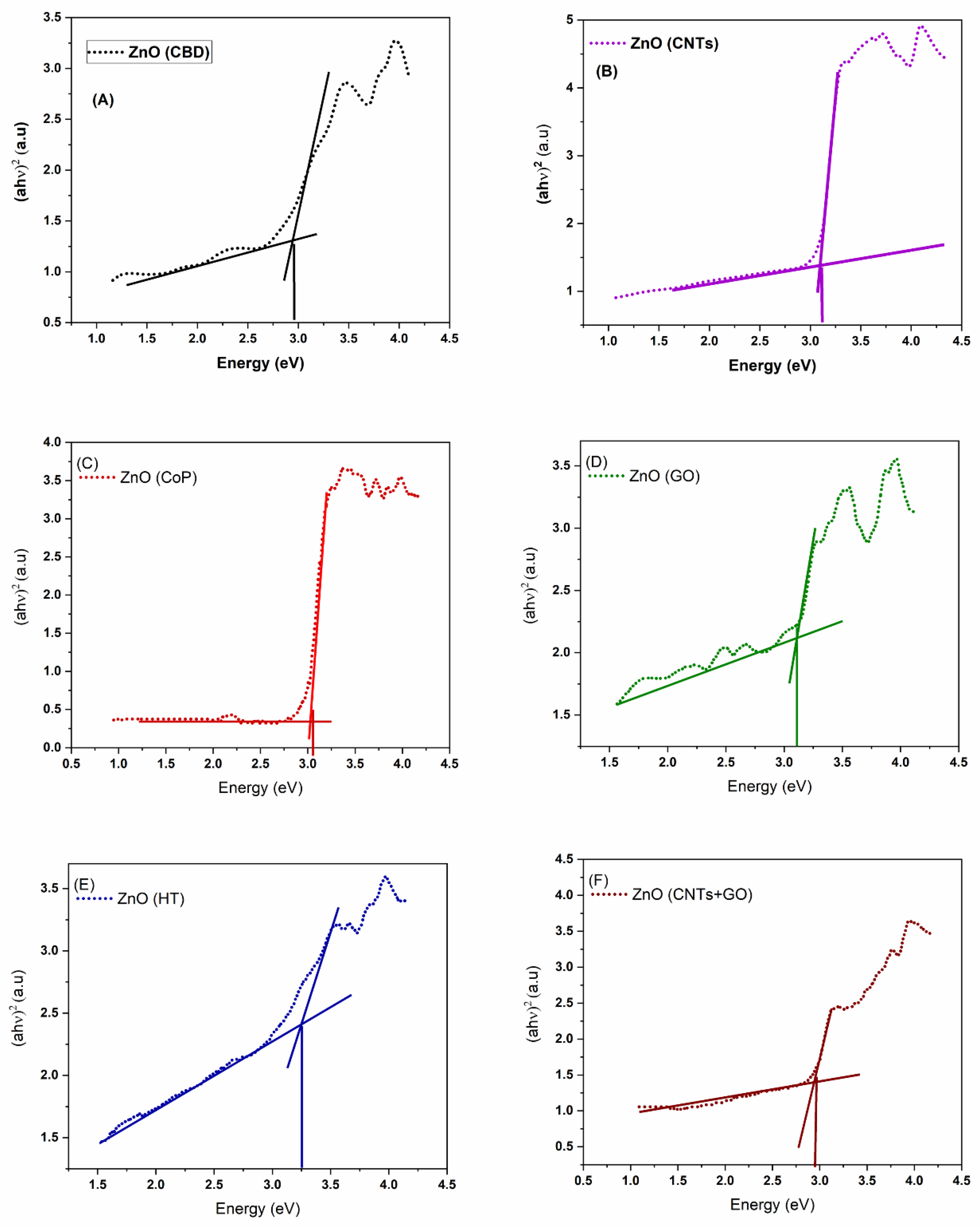
2.3. Band Gap Calculations
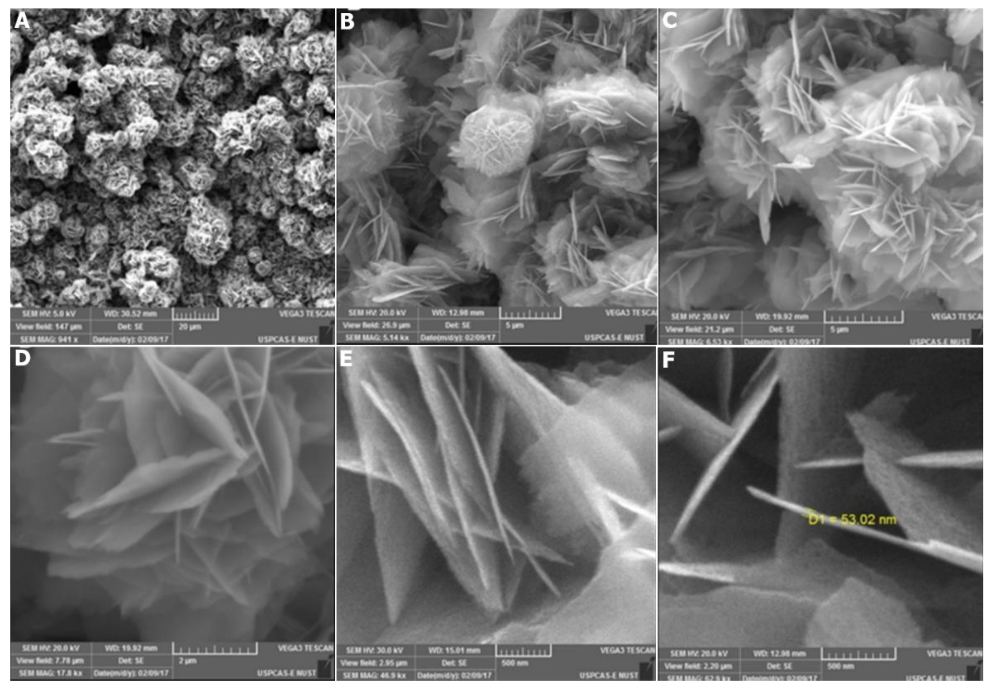
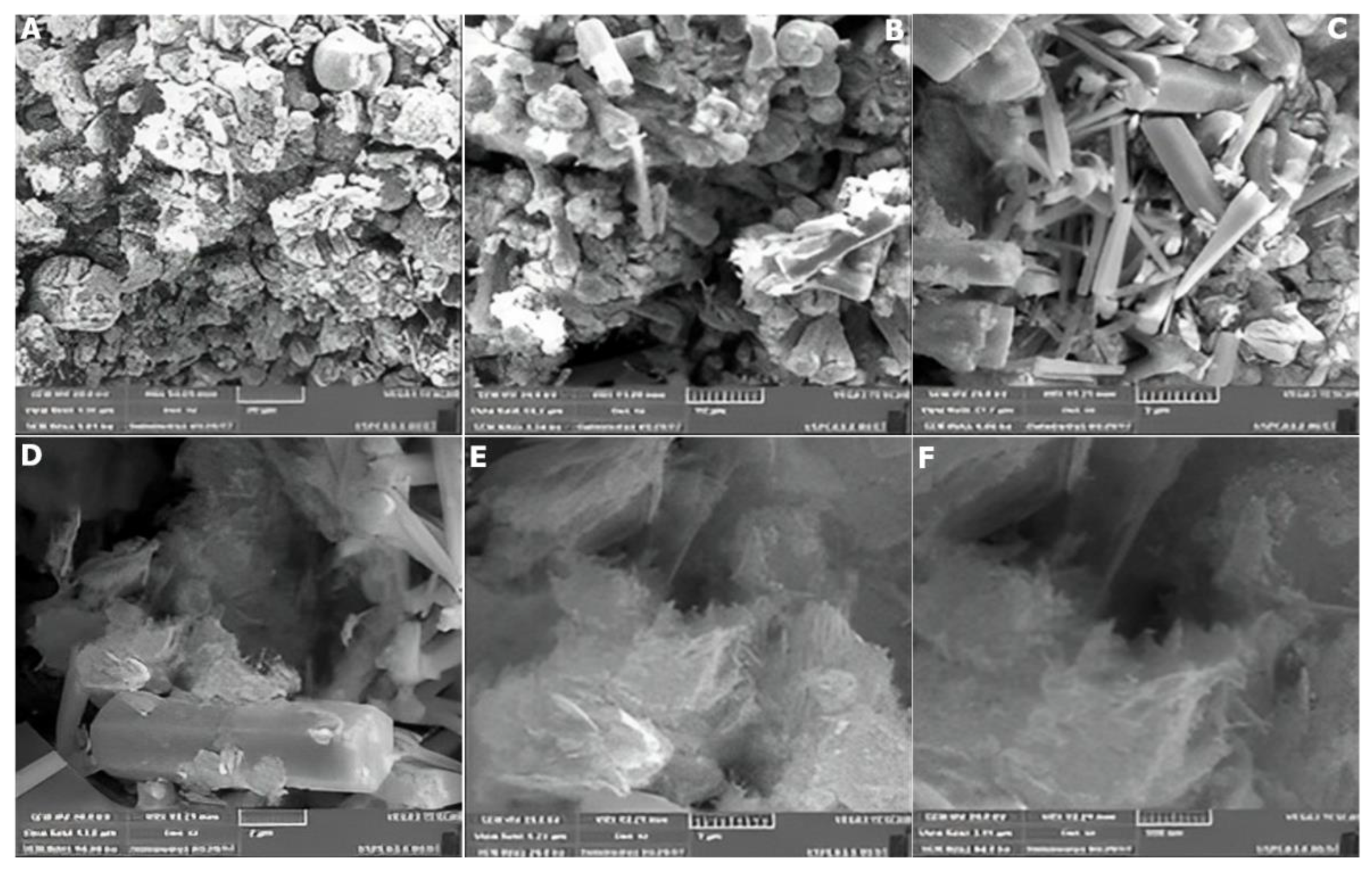
2.4. Morphology of ZnO Nanostructures
2.4.1. Morphology of ZnO Nanostructures Grown via the Hydrothermal Method
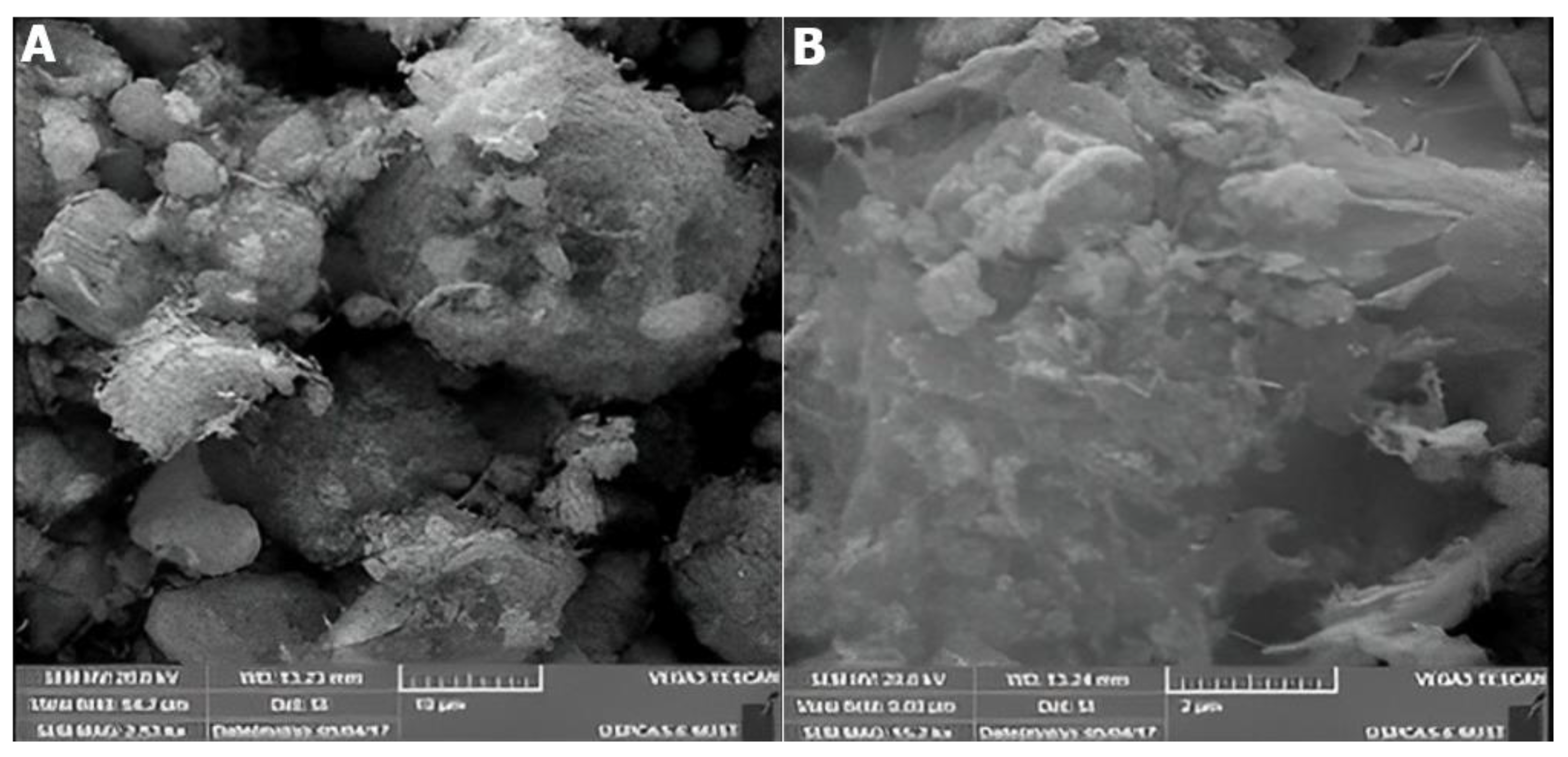
2.4.2. Morphology of ZnO Nanostructures Grown by Co-Precipitation Method
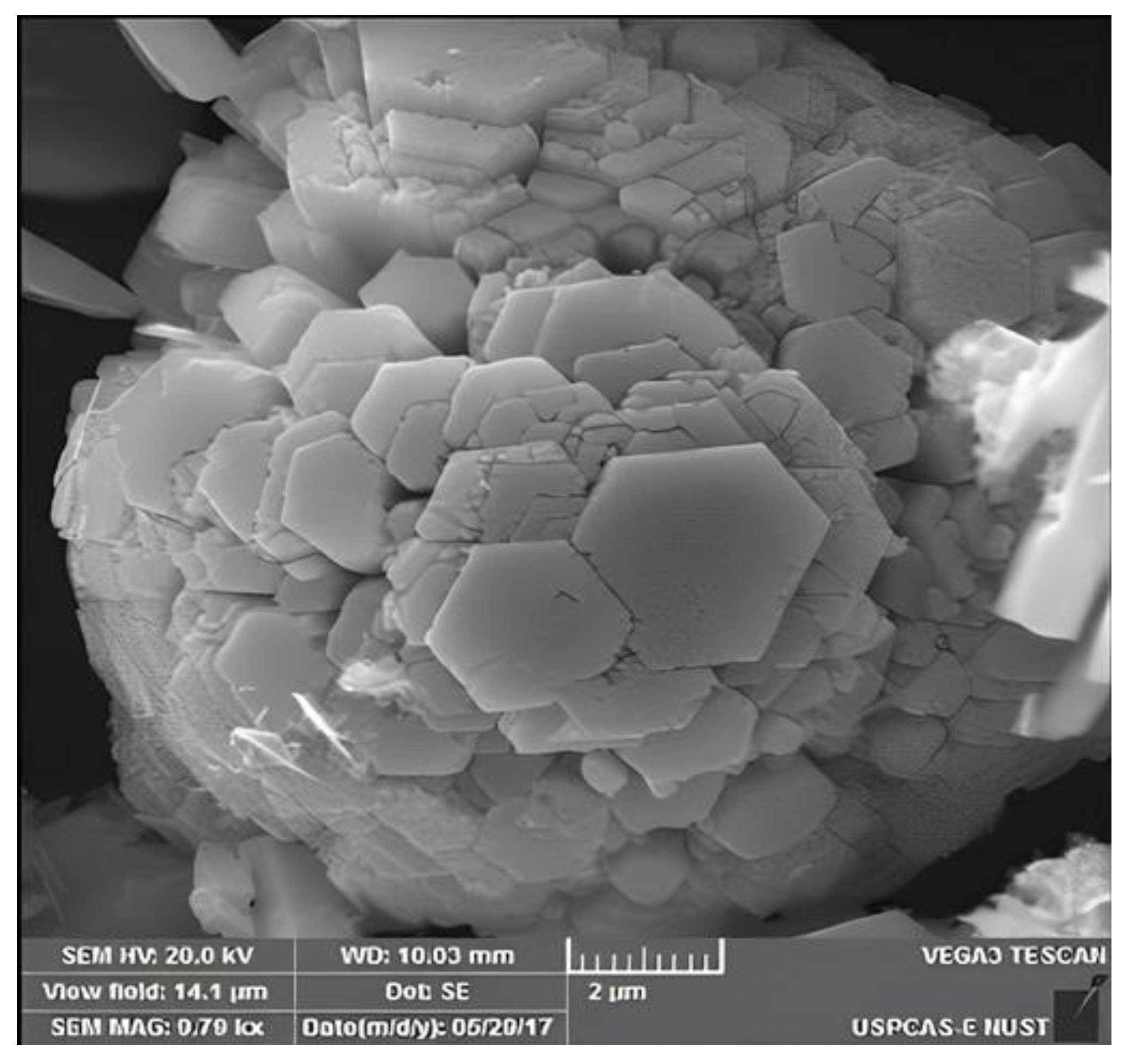
2.4.3. Morphology of ZnO Nanostructures Grown by Chemical Bath Deposition Method
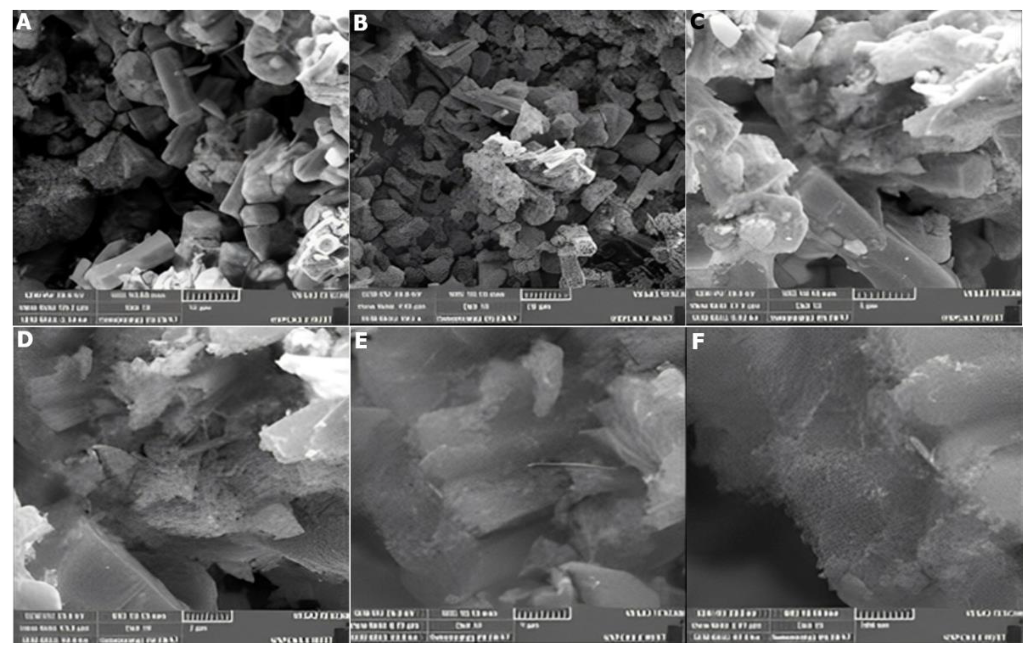
2.5. Morphology of ZnO/Carbon Nanocomposites Grown via the CBD Method
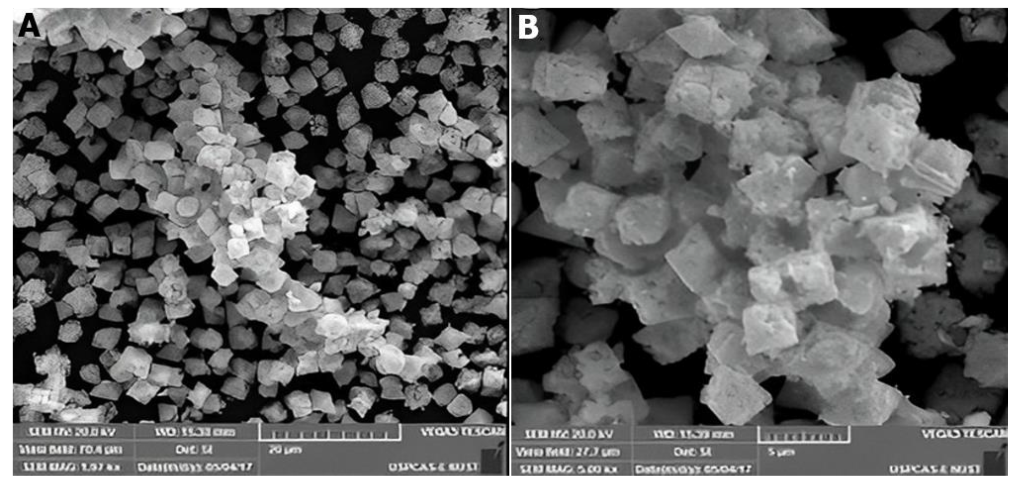
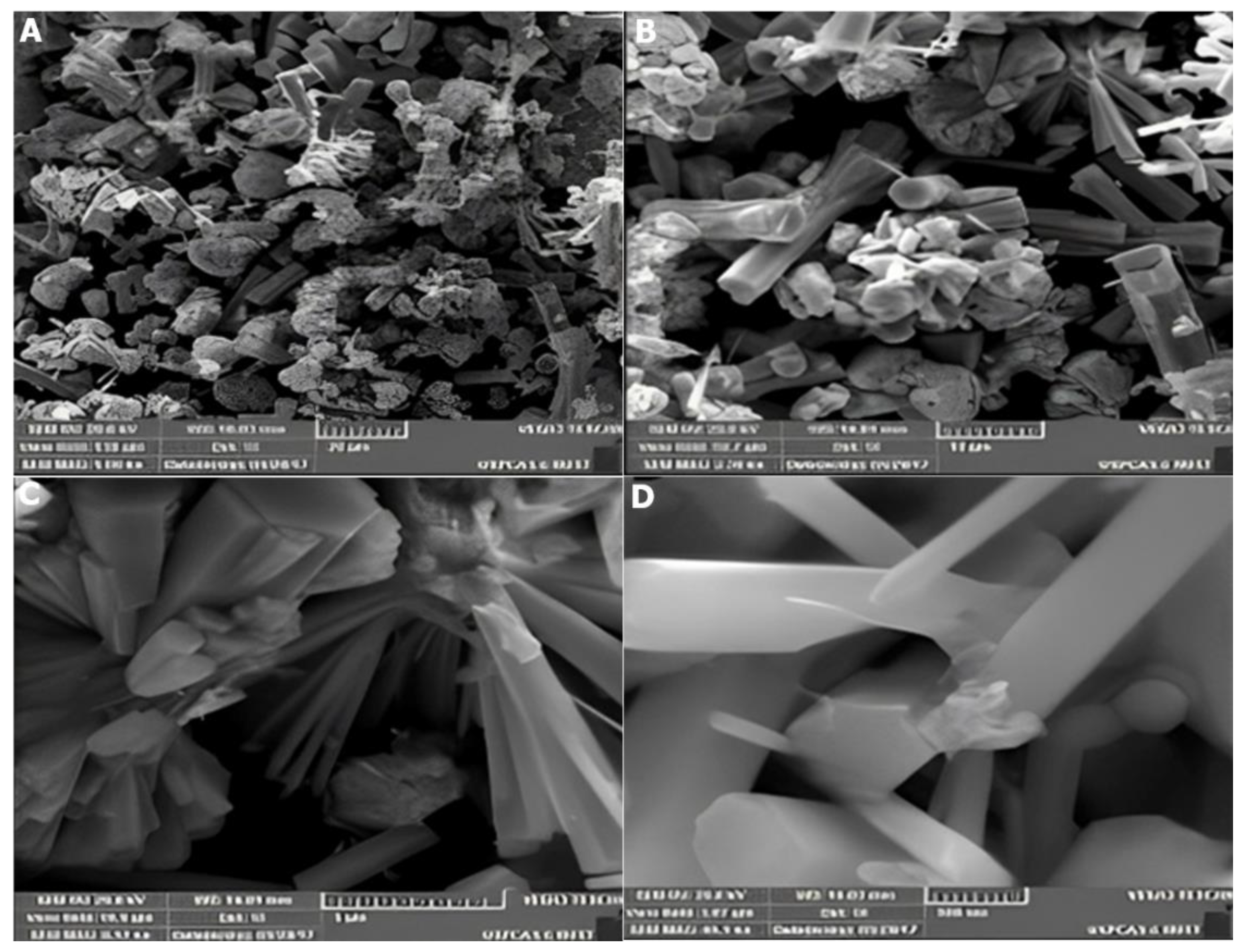
2.5.1. Morphology of ZnO/CNTs Nanocomposites
2.5.2. Morphology of ZnO/Graphene Oxide Nanocomposites
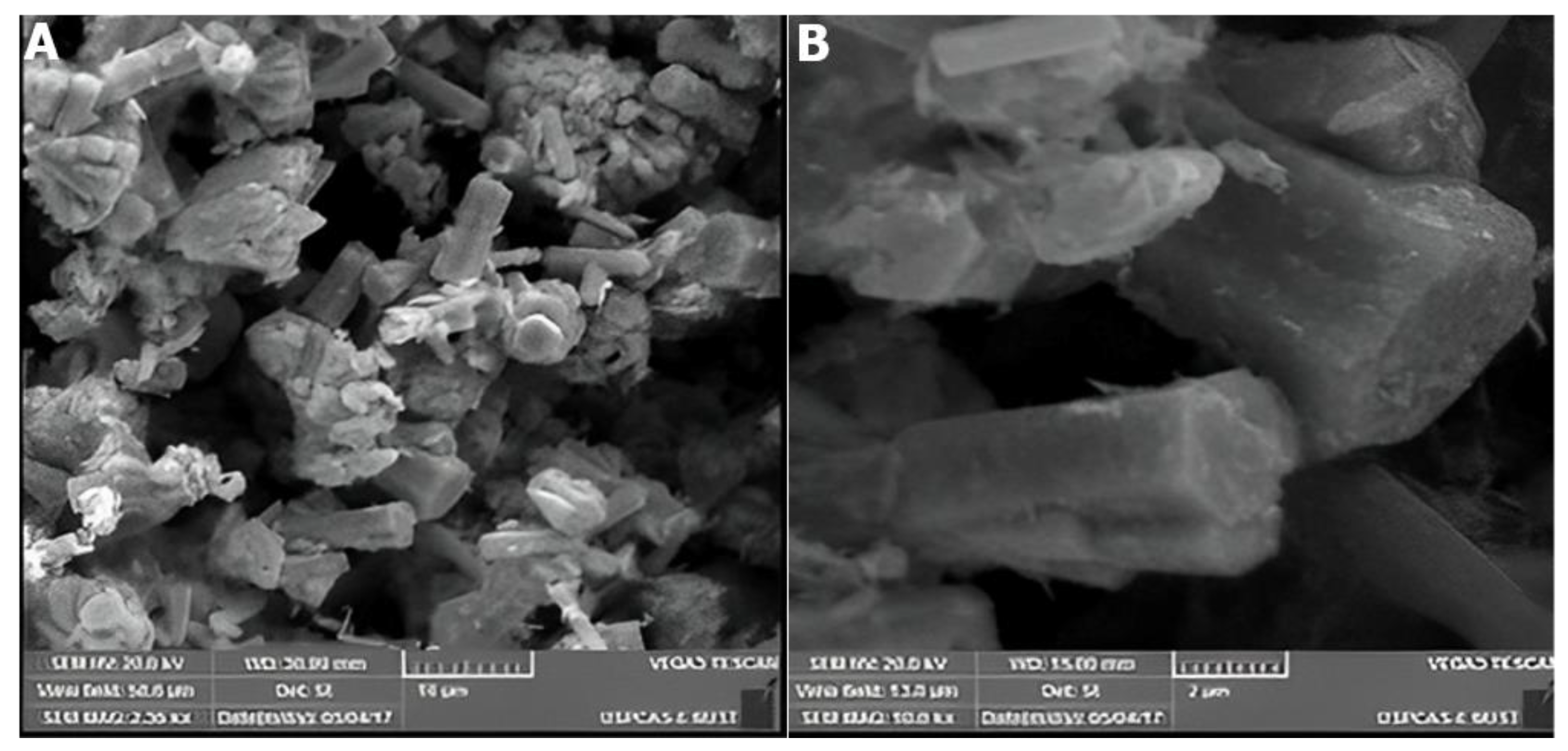
2.5.3. Morphology of ZnO/CNTs/GO Nanocomposites
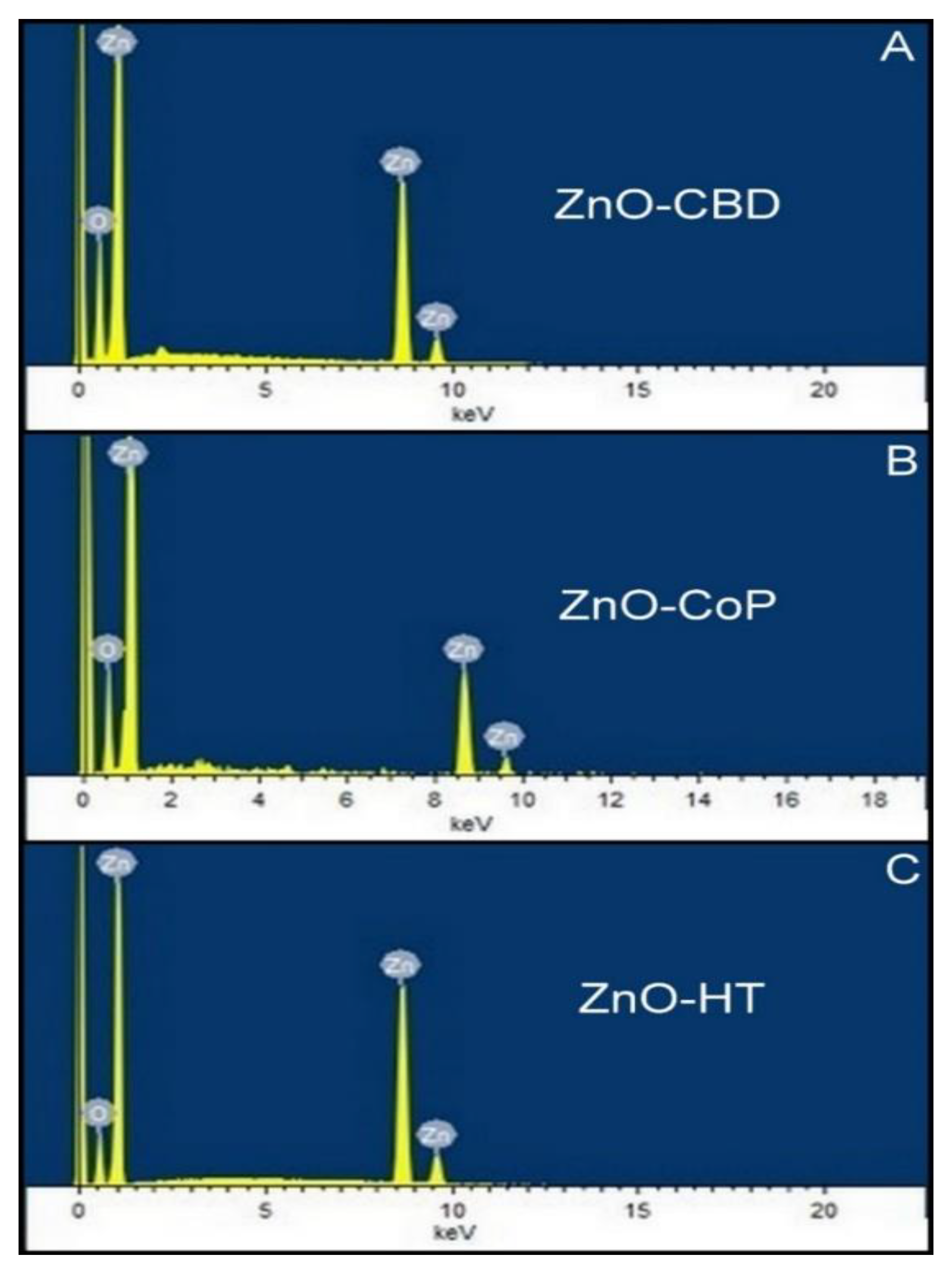
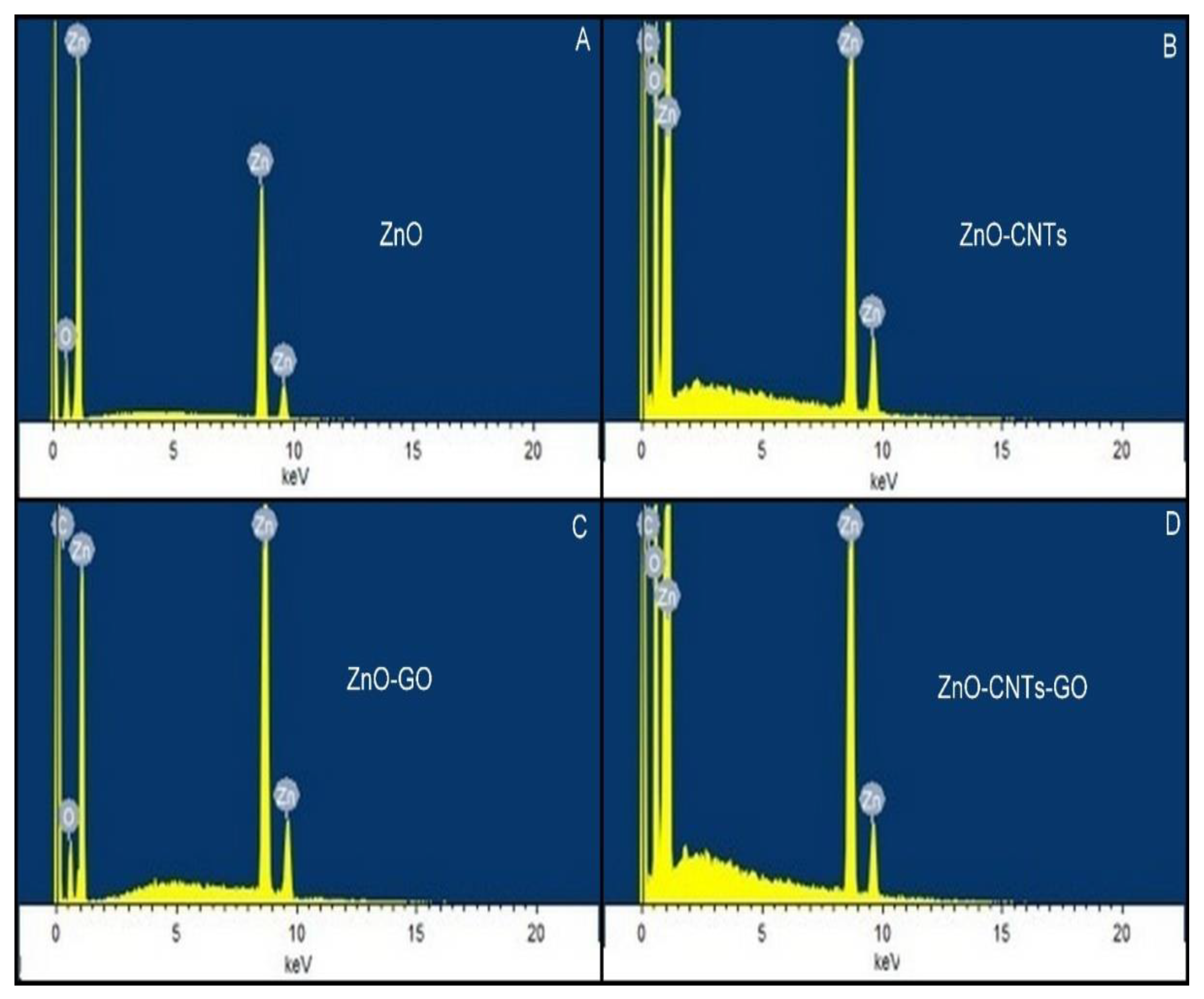
2.6. Energy Dispersive X-ray Spectroscopic (EDX) Analysis
2.6.1. EDX Analysis of ZnO Nanostructures
2.6.2. EDX Analysis of ZnO/CNTs/GO Nanocomposites
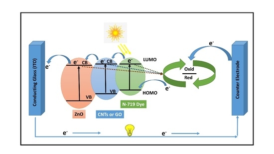
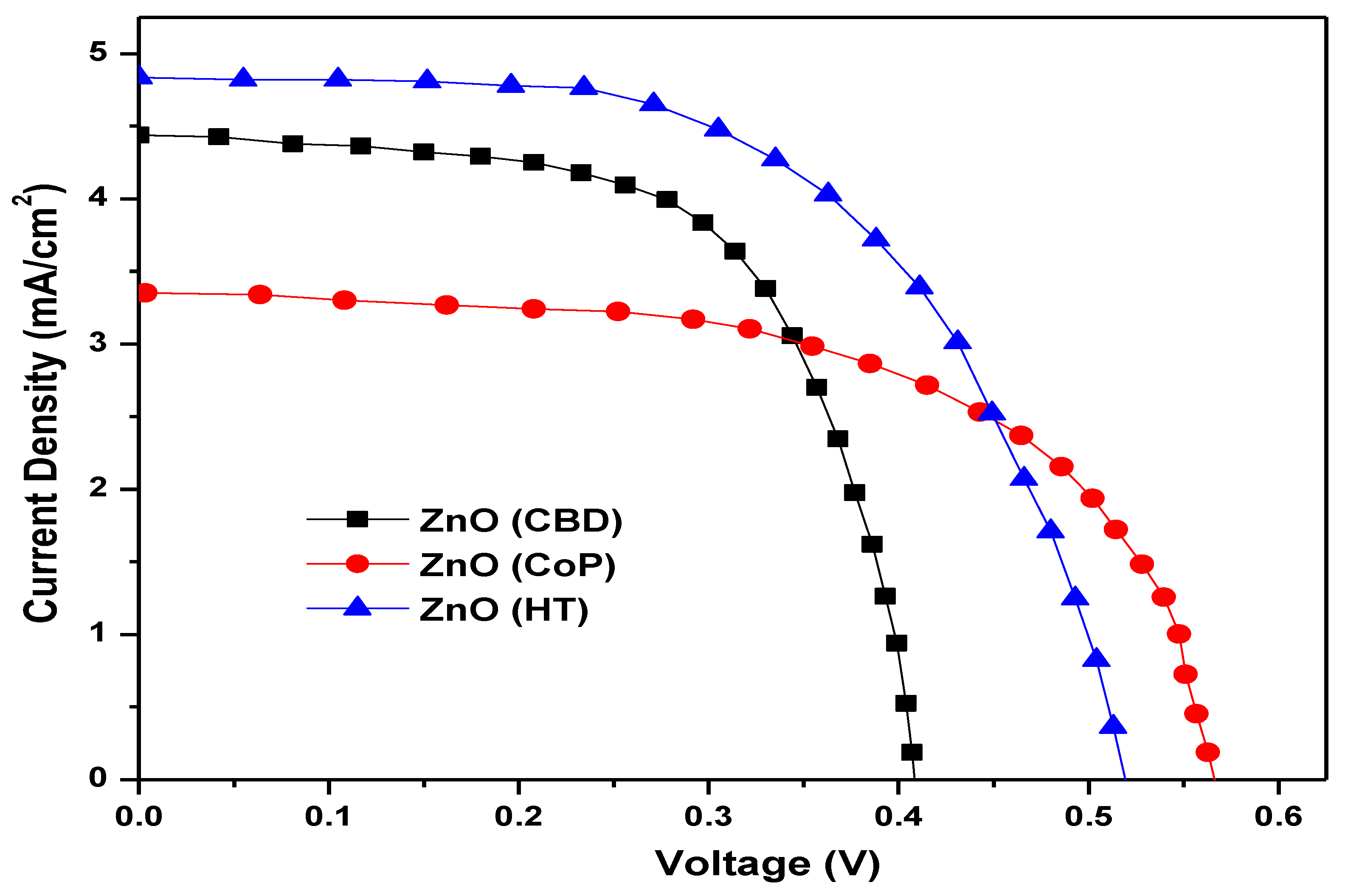
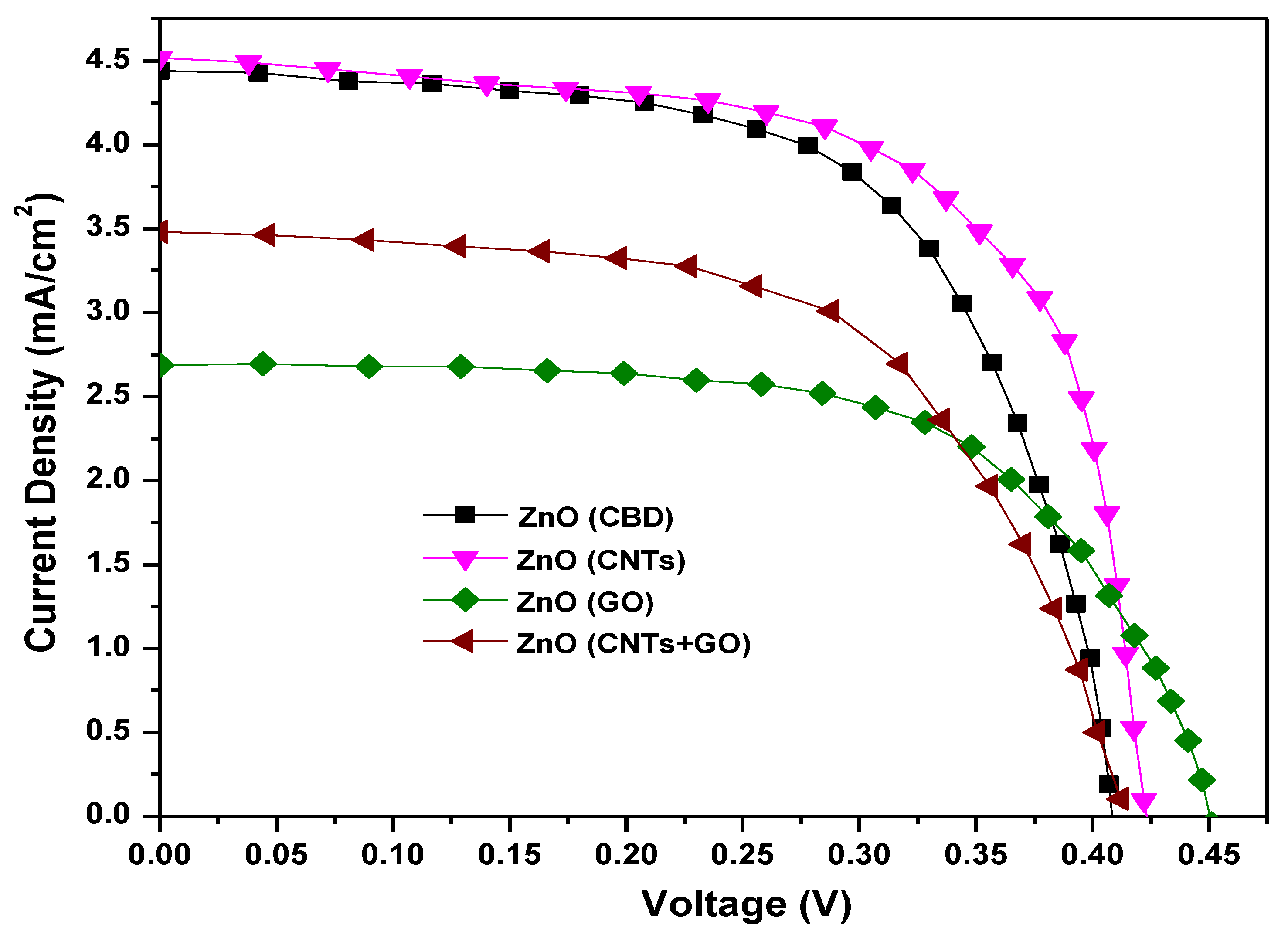
2.7. Current-Density Voltage Analysis of ZnO Based Dye Sensitized Solar Cells
3. Experimental
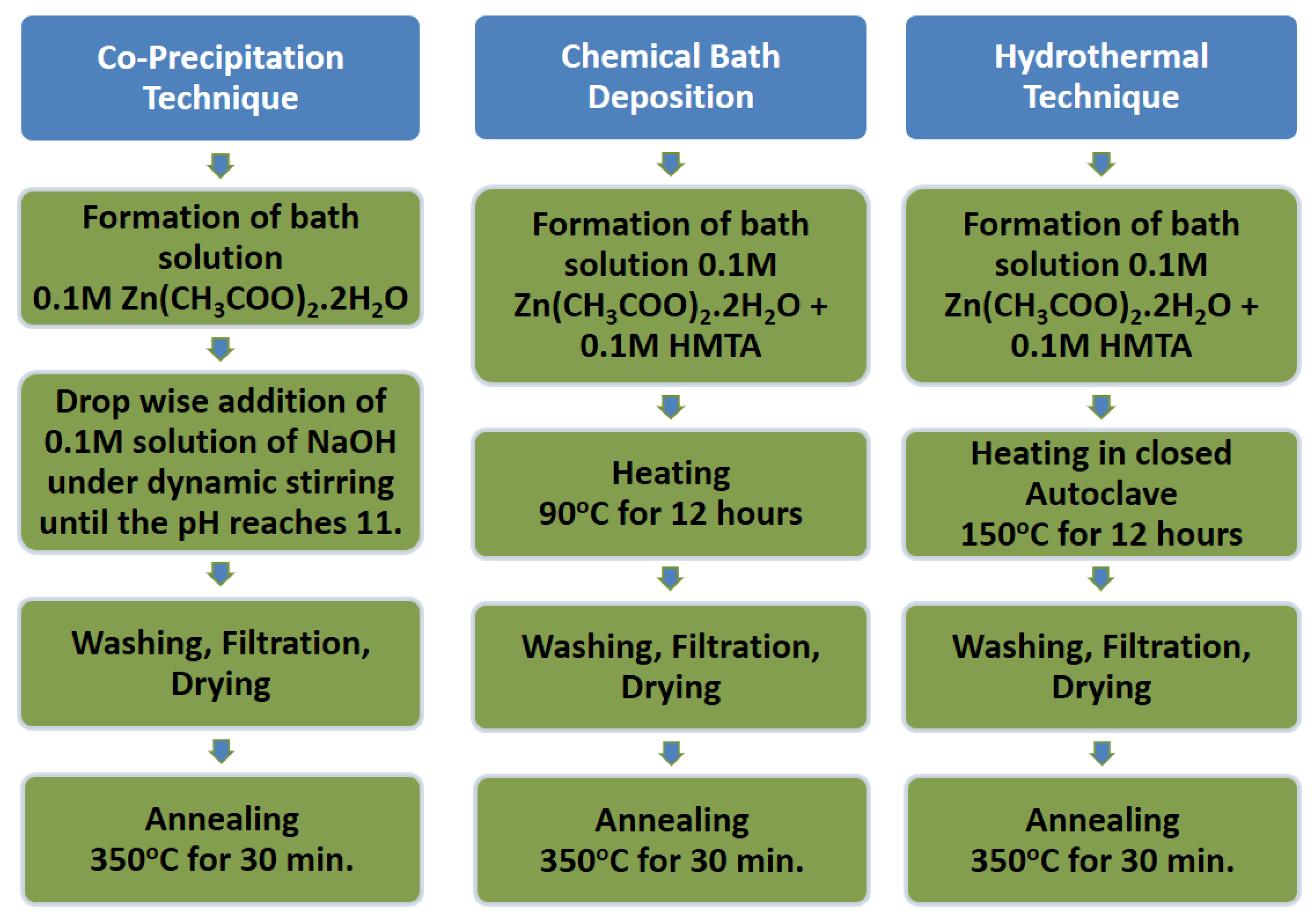
3.1. Materials and Synthesis Methods
3.2. Film Fabrication
3.3. Cell Fabrication
3.4. Characterization
4. Conclusions
Author Contributions
Funding
Acknowledgments
Conflicts of Interest
References
- Lee, T.H.; Sue, H.J.; Cheng, X. Solid-state dye-sensitized solar cells based on ZnO nanoparticle and nanorod array hybrid photoanodes. Nanoscale Res. Lett. 2011, 6, 517. [Google Scholar] [CrossRef] [PubMed] [Green Version]
- Barber, G.D.; Hoertz, P.G.; Lee, S.-H.A.; Abrams, N.M.; Mikulca, J.; Mallouk, T.E.; Liska, P.; Zakeeruddin, S.M.; Gratzel, M.; Ho-Baillie, A.; et al. Utilization of Direct and Diffuse Sunlight in a Dye-Sensitized Solar Cell—Silicon Photovoltaic Hybrid Concentrator System. J. Phys. Chem. Lett. 2011, 2, 581–585. [Google Scholar] [CrossRef]
- Klaus, J.; Isabella, O.; Smets, A.H.M.; Swaaij., R.A.C.M.M.; Zeman, M. Solar Energy Fundamentals, Technology, and Systems; Delft University of Technology: Delft, The Netherlands, 2014. [Google Scholar]
- O’Regan, B.; Gratzel, M. A low-cost, high-efficiency solar cell based on dye-sensitized colloidal TiO2 films. Nature 1991, 353, 737–740. [Google Scholar] [CrossRef]
- Grätzel, M. Dye-sensitized solar cells. J. Photochem. Photobiol. C Photochem. Rev. 2003, 4, 145–153. [Google Scholar] [CrossRef]
- Al, N.; Hussain, A.; Ahmed, R.; Wang, M.K.; Zhao, C.; Haq, B.U.; Fu, Y.Q. Advances in nanostructured thin film materials for solar cell applications. Renew. Sustain. Energy Rev. 2016, 59, 726–737. [Google Scholar] [CrossRef]
- Albero, J.; Atienzar, P.; Corma, A.; Garcia, H. Efficiency Records in Mesoscopic Dye-Sensitized Solar Cells. Chem. Rec. 2015, 15, 803–828. [Google Scholar] [CrossRef] [PubMed]
- Liu, X.; Fang, J.; Liu, Y.; Lin, T. Progress in nanostructured photoanodes for dye-sensitized solar cells. Front. Mater. Sci. 2016, 10, 225–237. [Google Scholar] [CrossRef]
- Memarian, N.; Concina, I.; Braga, A.; Rozati, S.M.; Vomiero, A.; Sberveglieri, G. Hierarchically Assembled ZnO Nanocrystallites for High-Efficiency Dye-Sensitized Solar Cells. Angew. Chem. Int. Ed. 2011, 50, 12321–12325. [Google Scholar] [CrossRef]
- Martinson, A.B.F.; Elam, J.W.; Hupp, J.T.; Pellin, M.J. ZnO Nanotube Based Dye-Sensitized Solar Cells. Nano Lett. 2007, 7, 2183–2187. [Google Scholar] [CrossRef]
- Martinson, A.B.F.; McGarrah, J.E.; Parpia, M.O.K.; Hupp, J.T. Dynamics of charge transport and recombination in ZnO nanorod array dye-sensitized solar cells. Phys. Chem. Chem. Phys. 2006, 8, 4655–4659. [Google Scholar] [CrossRef]
- Qiu, Y.; Yang, S. ZnO Nanotetrapods: Controlled Vapor-Phase Synthesis and Application for Humidity Sensing. Adv. Funct. Mater. 2007, 17, 1345–1352. [Google Scholar] [CrossRef]
- Zhang, W.; Wang, P.; Fei, X.; Xiu, Y.; Jia, G. Growth Mechanism and Morphologies Tuning of ZnO Nanostructures. Int. J. Electrochem. Sci. 2015, 10, 4688–4695. [Google Scholar]
- Zhang, Q.; Dandeneau, C.S.; Zhou, X.; Cao, G. ZnO Nanostructures for Dye-Sensitized Solar Cells. Adv. Mater. 2009, 21, 4087–4108. [Google Scholar] [CrossRef]
- Wang, Z.L. Zinc oxide nanostructures: Growth, properties and applications. J. Phys. Condens. Matter 2004, 16, R829–R858. [Google Scholar] [CrossRef]
- Tyona, M.D.; Osuji, R.U.; Ezema, F.I. A review of zinc oxide photoanode films for dye-sensitized solar cells based on zinc oxide nanostructures. Adv. Nano Res. 2013, 1, 43–58. [Google Scholar] [CrossRef] [Green Version]
- Yun, Y.S.; Park, J.Y.; Oh, H.; Kim, J.J.; Kim, S.S. Electrical transport properties of size-tuned ZnO nanorods. J. Mater. Res. 2006, 21, 132–136. [Google Scholar] [CrossRef]
- Yi, G.C.; Wang, C.; Park, W.I. ZnO nanorods: Synthesis, characterization and applications. Semicond. Sci. Technol. 2005, 20, S22–S34. [Google Scholar] [CrossRef]
- Kong, X.Y.; Wang, Z.L. Spontaneous Polarization-Induced Nanohelixes, Nanosprings, and Nanorings of Piezoelectric Nanobelts. Nano Lett. 2003, 3, 1625–1631. [Google Scholar] [CrossRef] [Green Version]
- Kong, X.Y.; Ding, Y.; Yang, R.; Wang, Z.L. Single-Crystal Nanorings Formedby Epitaxial Self-Coiling of Polar Nanobelts. Science 2004, 303, 1348–1351. [Google Scholar] [CrossRef] [Green Version]
- Wang, J.S.; Yang, C.S.; Chen, P.I.; Su, C.F.; Chen, W.J.; Chiu, K.C.; Chou, W.C. Catalyst-free highly vertically aligned ZnO nanoneedle arrays grown by plasma-assisted molecular beam epitaxy. Appl. Phys. A 2009, 97, 553–557. [Google Scholar] [CrossRef]
- Wahab, R.; Ansari, S.G.; Kim, Y.S.; Seo, H.K.; Shin, H.S. Room temperature synthesis of needle-shaped ZnO nanorods via sonochemical method. Appl. Surf. Sci. 2007, 253, 7622–7626. [Google Scholar] [CrossRef]
- Satoh, Y.; Ohshio, S.; Saitoh, H. Photoluminescence spectroscopy of highly oriented Y2O3: Tb crystalline whiskers. Sci. Technol. Adv. Mater. 2016, 6, 215–218. [Google Scholar] [CrossRef] [Green Version]
- Hu, J.Q.; Bando, Y. Growth and optical properties of single-crystal tubular ZnO whiskers. Appl. Phys. Lett. 2003, 82, 1401–1403. [Google Scholar] [CrossRef]
- Gao, P.X.; Wang, Z.L. Mesoporous Polyhedral Cages and Shells Formed by Textured Self-Assembly of ZnO Nanocrystals. J. Am. Chem. Soc. 2003, 125, 11299–11305. [Google Scholar] [CrossRef] [PubMed]
- Ding, G.Q.; Shen, W.Z.; Zheng, M.J.; Fan, D.H. Synthesis of ordered large-scale ZnO nanopore arrays. Appl. Phys. Lett. 2006, 88, 103106. [Google Scholar] [CrossRef] [Green Version]
- Wan, Q.; Wang, T.H.; Zhao, J.C. Enhanced photocatalytic activity of ZnO nanotetrapods. Appl. Phys. Lett. 2005, 87, 083105. [Google Scholar] [CrossRef]
- Gao, P.X.; Wang, Z.L. Nanopropeller arrays of zinc oxide. Appl. Phys. Lett. 2004, 84, 2883–2885. [Google Scholar] [CrossRef] [Green Version]
- Yang, P.; Yan, H.; Mao, S.; Russo, R.; Johnson, J.; Saykally, R.; Morris, N.; Pham, J.; He, R.; Choi, H.J. Controlled Growth of ZnO Nanowires and Their Optical Properties. Adv. Funct. Mater. 2002, 12, 323–331. [Google Scholar] [CrossRef]
- Wang, Z.L. Novel Zinc Oxide Nanostructures Discovery by Electron Microscopy. J. Phys. Conf. Ser. 2006, 26, 1–6. [Google Scholar] [CrossRef] [Green Version]
- Xu, C.X.; Sun, X.W. Field emission from zinc oxide nanopins. Appl. Phys. Lett. 2003, 83, 3806–3808. [Google Scholar] [CrossRef]
- Lao, J.Y.; Haung, J.Y.; Ren, Z.F. ZnO Nanobridges and Nanonails. Nano Lett. 2003, 3, 235–238. [Google Scholar] [CrossRef]
- Lao, C.S.; Shi, L.C.; Gao, P.X.; Sen, Y.R.; Yue, Z.; Ying, D.; Wang, Z.L. Formation of double-side teethed nanocombs of ZnO and self-catalysis of Zn-terminated polar surface. Chem. Phys. Lett. 2006, 417, 358–362. [Google Scholar] [CrossRef]
- Yang, Z.; Xu, T.; Ito, Y.; Welp, U.; Kwok, W.K. Enhanced Electron Transport in Dye-Sensitized Solar Cells UsingShort ZnO Nanotips on A Rough Metal Anode. J. Phys. Chem. C 2009, 113, 20521–20526. [Google Scholar] [CrossRef]
- Xu, C.X.; Xu, C.X.; Sun, X.W.; Dong, Z.L.; Yu, M.B. Zinc oxide nanodisk. Appl. Phys. Lett. 2004, 85, 3878–3880. [Google Scholar] [CrossRef]
- Hu, J.Q.; Li, Q.; Meng, X.M.; Lee, C.S.; Lee, S.T. Thermal Reduction Route to the Fabrication of Coaxial Zn/ZnO Nanocables and ZnO Nanotubes. Chem. Mater. 2003, 15, 305–308. [Google Scholar] [CrossRef]
- Hu, J.Q.; Bando, Y.; Zhan, J.H.; Li, Y.B.; Sekiguchi, T. Two-dimensional micrometer-sized single-crystalline ZnO thin nanosheets. Appl. Phys. Lett. 2003, 83, 4414. [Google Scholar] [CrossRef]
- Jiang, C.Y.; Sun, X.W.; Lo, G.Q.; Kwong, D.L. Improved dye-sensitized solar cells with a ZnO-nanoflower photoanode. Appl. Phys. Lett. 2007, 90, 263501. [Google Scholar] [CrossRef]
- Abdullah, H.; Ariyanto, N.P.; Shaari, S.; Yuliarto, B.; Junaidi, S. Study of porous nanoflake ZnO for dye-sensitized solar cell application. Am. J. Eng. Appl. Sci. 2009, 2, 236–240. [Google Scholar]
- Radzimska, A.K.; Jesionowski, T. Zinc Oxide-From Synthesis to Application: A Review. Materials 2014, 7, 2833–2881. [Google Scholar] [CrossRef] [Green Version]
- Wu, C.-T.; Liao, W.-P.; Wu, J.-J. Three-dimensional ZnO nanodendrite/nanoparticle composite solar cells. J. Mater. Chem. 2011, 21, 2871–2876. [Google Scholar] [CrossRef]
- Chang, W.-C.; Cheng, Y.Y.; Yu, W.C.; Yao, Y.C.; Lee, C.H.; Ko, H.H. Enhancing performance of ZnO dye-sensitized solar cells by incorporation of multiwalled carbon nanotubes. Nanoscale Res. Lett. 2012, 7, 166. [Google Scholar] [CrossRef] [PubMed] [Green Version]
- Chindaduang, A.; Duangkaew, P.; Pratontep, S.; Tumcharern, G. Effects of Multi-walled Carbon Nanotube Incorporation in ZnO Photoelectrode on the Efficiency of Dye-Sensitized Solar Cells. NU Sci. J. 2009, 6, 28–35. [Google Scholar]
- Chindaduang, A.; Duangkaew, P.; Pratontep, S.; Tumcharern, G. Structural, Optical and Photovoltaic Properties of ZnO-MWCNTs Electrodes. J. Microsc. Soc. Thail. 2009, 23, 115–118. [Google Scholar]
- Dai, L.; Chang, D.W.; Baek, J.B.; Lu, W. Carbon nanomaterials for advanced energy conversion and storage. Small 2012, 8, 1130–1166. [Google Scholar] [CrossRef] [PubMed]
- Zhu, H.; Wei, J.; Wang, K.; Wu, A. Applications of carbon materials in photovoltaic solar cells. Sol. Energy Mater. Sol. Cells 2009, 93, 1461–1470. [Google Scholar] [CrossRef]
- Ghai, P.; Kesarwani, A.; Kansal, S. Carbon Nanotubes in Photovoltaics. Int. Adv. Res. J. Sci. Eng. Technol. 2015, 2, 125–128. [Google Scholar]
- Yen, C.Y.; Lin, Y.F.; Liao, S.H.; Weng, C.C.; Huang, C.C.; Hsiao, Y.H.; Ma, C.C.M.; Chang, M.C.; Shao, H.; Tsai, M.C.; et al. Preparation and properties of a carbon nanotube-based nanocomposite photoanode for dye-sensitized solar cells. Nanotechnology 2008, 19, 375305. [Google Scholar] [CrossRef]
- Ramar, A.; Soundappan, T.; Chen, S.M.; Rajkumar, M.; Ramiah, S. Incorporation of Multi-Walled Carbon Nanotubes in ZnO for Dye Sensitized Solar Cells. Int. J. Electrochem. Sci. 2012, 7, 11734–11744. [Google Scholar]
- Saito, M.; Fujihara, S. Fabrication and photovoltaic properties of dye-sensitized ZnO thick films by a facile doctor-blade printing method using nanocrystalline pastes. J. Ceram. Soc. Japan. 2009, 117, 823–827. [Google Scholar] [CrossRef] [Green Version]
- Wu, J.J.; Chen, G.R.; Yang, H.H.; Ku, C.H.; Lai, J.Y. Effects of dye adsorption on the electron transport properties in ZnO-nanowire dye-sensitized solar cells. Appl. Phys. Lett. 2007, 90, 213109. [Google Scholar] [CrossRef]
- Keis, K.; Jan Lindgren, J.; Lindquist, S.E.; Hagfeldt, A. Studies of the Adsorption Process of Ru Complexes in Nanoporous ZnO Electrodes. Langmuir 2000, 16, 4688–4694. [Google Scholar] [CrossRef]
- Lamberti, A.; Sacco, A.; Bianco, S.; Giuri, E.; Quaglio, M.; Chiodoni, A.; Tresso, E. Microfluidic sealing and housing system for innovative dye-sensitized solar cell architecture. Microelectron. Eng. 2011, 88, 2308–2310. [Google Scholar] [CrossRef]


| Samples | Peak Width (FWHM) | Peak Position (2θ) | Crystallite Size (nm) |
|---|---|---|---|
| ZnO (CBD) | 0.17 | 36.2 | ~51.37 |
| ZnO (CoP) | 0.24 | 36.2 | ~36.39 |
| ZnO (HT) | 0.50 | 36.2 | ~17.47 |
| ZnO (CNTs) | 0.18 | 36.2 | ~48.51 |
| ZnO(GO) | 0.19 | 36.2 | ~45.96 |
| ZnO (CNTs + GO) | 0.18 | 36.2 | ~48.51 |
| Samples | Band Gap Values Using F(R) Spectra | Band Gap Values Using T and R Spectra | ||
|---|---|---|---|---|
| Band Gap (eV) | Error (eV) | Band Gap (eV) | Error (eV) | |
| ZnO (CBD) | 3.15 | ±0.05 | 3.20 | ±0.08 |
| ZnO (CoP) | 3.20 | ±0.05 | 3.20 | ±0.08 |
| ZnO (HT) | 3.21 | ±0.05 | 3.21 | ±0.08 |
| ZnO/CNTs | 3.20 | ±0.05 | 3.19 | ±0.08 |
| ZnO/GO | 3.19 | ±0.05 | 3.18 | ±0.08 |
| ZnO/CNTs/GO | 3.18 | ±0.05 | 3.19 | ±0.08 |
| Samples | VOC (V) | JSC (mA/cm2) | Vmp (V) | Jmp (mA/cm2) | FF | η (%) |
|---|---|---|---|---|---|---|
| ZnO (HT) | 0.513 | 4.89 | 0.363 | 4.02 | 0.59 | 1.99 |
| ZnO (CoP) | 0.568 | 3.34 | 0.415 | 2.17 | 0.59 | 1.50 |
| ZnO (CBD) | 0.407 | 4.42 | 0.314 | 3.63 | 0.63 | 1.52 |
| ZnO (CNTs) | 0.422 | 4.49 | 0.322 | 3.85 | 0.65 | 1.66 |
| ZnO (GO) | 0.451 | 2.67 | 0.328 | 2.34 | 0.64 | 1.02 |
| ZnO (CNTs + GO) | 0.412 | 3.45 | 0.317 | 2.74 | 0.61 | 1.16 |
Publisher’s Note: MDPI stays neutral with regard to jurisdictional claims in published maps and institutional affiliations. |
© 2022 by the authors. Licensee MDPI, Basel, Switzerland. This article is an open access article distributed under the terms and conditions of the Creative Commons Attribution (CC BY) license (https://creativecommons.org/licenses/by/4.0/).
Share and Cite
Gulab, H.; Fatima, N.; Shahzad, N.; Shahzad, M.I.; Siddique, M.; Hussain, M.; Humayun, M. Fabrication of Carbon/Zinc Oxide Nanocomposites as Highly Efficient Catalytic Materials for Application in Dye-Sensitized Solar Cells. Catalysts 2022, 12, 1354. https://doi.org/10.3390/catal12111354
Gulab H, Fatima N, Shahzad N, Shahzad MI, Siddique M, Hussain M, Humayun M. Fabrication of Carbon/Zinc Oxide Nanocomposites as Highly Efficient Catalytic Materials for Application in Dye-Sensitized Solar Cells. Catalysts. 2022; 12(11):1354. https://doi.org/10.3390/catal12111354
Chicago/Turabian StyleGulab, Hussain, Nusrat Fatima, Nadia Shahzad, Muhammad Imran Shahzad, Mohsin Siddique, Muhammad Hussain, and Muhammad Humayun. 2022. "Fabrication of Carbon/Zinc Oxide Nanocomposites as Highly Efficient Catalytic Materials for Application in Dye-Sensitized Solar Cells" Catalysts 12, no. 11: 1354. https://doi.org/10.3390/catal12111354