Article

Nanoscale Assembly of BiVO4/CdS/CoOx Core–Shell Heterojunction for Enhanced Photoelectrochemical Water Splitting

1
Regional Centre of Advanced Technologies and Materials, Czech Advanced Technology and Research Institute, Palacky University Olomouc, Křížkovského 511/8, 779 00 Olomouc, Czech Republic
2
HEKA Elektronik GmbH, Wiesenstrasse 55, 67466 Lambrecht, Germany
3
CEET, Nanotechnology Centre, Centre of Energy and Environmental Technologies, VŠB−Technical University of Ostrava, 17. Listopadu 2172/15, 708 00 Ostrava-Poruba, Czech Republic
4
Department of Materials Science and Engineering, University of Erlangen-Nuremberg, Martensstrasse 7, 91058 Erlangen, Germany
5
Institute of Fundamental and Frontier Sciences, University of Electronic Science and Technology of China, Chengdu 610054, China
*
Authors to whom correspondence should be addressed.
Authors with equal contribution.
Catalysts 2021, 11(6), 682; https://doi.org/10.3390/catal11060682
Submission received: 3 May 2021 / Revised: 21 May 2021 / Accepted: 24 May 2021 / Published: 28 May 2021

Abstract

:
Porous BiVO4 electrodes were conformally decorated with CdS via a chemical bath deposition process. The highest photocurrent at 1.1 V vs. RHE was achieved for a BiVO4/CdS composite (4.54 mA cm−2), compared with CdS (1.19 mA cm−2) and bare BiVO4 (2.1 mA cm−2), under AM 1.5G illumination. This improvement in the photoefficiency can be ascribed to both the enhanced optical absorption properties and the charge separation due to the heterojunction formation between BiVO4 and CdS. Furthermore, the BiVO4/CdS photoanode was protected with a CoOx layer to substantially increase the photostability of the material. The new BiVO4/CdS/CoOx nanostructure exhibited a highly stable photocurrent density of ~5 mA cm−2. The capability to produce O2 was locally investigated by scanning photoelectrochemical microscope, which showed a good agreement between photocurrent and O2 reduction current maps. This work develops an efficient route to improve the photo-electrochemical performance of BiVO4 and its long-term stability.

Graphical Abstract

1. Introduction

In the recent past, the development of efficient energy conversion/storage devices has received a great deal of attention from the community of scientific and technological researchers. The dramatically increased demand of our society for accessible energy sources and the related concerns for the environment further impelled such attempts [1,2]. In this context, the design and development of cost-competitive materials capable of producing fuels and electricity directly from the energy harvested from sunlight offer a desirable approach to fulfilling the need for clean and sustainable energy [1,3,4]. Photoactive semiconductors (e.g., TiO2, WO3, or ZnO) are widely used materials for the conversion of solar light into storable and transportable chemical energy such as dihydrogen (H2) via the process of photoelectrochemical splitting of water (PEC-WS) where they serve as photoanodes [5,6]. The advantages of these metal oxides lie in their general abundance, relatively easy processability, and remarkable chemical as well as PEC stability even in harsh electrolyte environments. On the other hand, the main drawback that significantly limits their practical utilization for a large-scale industrial production of H2 is their wide bandgap (e.g., 3.0–3.2 eV for TiO2, 2.7 eV for WO3, and 3.1–3.3 eV for ZnO), which is translated into poor absorption of the solar spectrum, hence the low PEC-WS efficiency [6,7]. In contrast, bismuth vanadate (BiVO4) has a significantly narrower bandgap energy, around 2.4–2.5 eV, and simultaneously shows a good stability and enables low-cost production [8,9]. The application of BiVO4 for solar water oxidation was first reported by Kudo et al. in 1998 [10]. Since then, photoanodes based on n-type BiVO4 have been continuously and extensively studied. Several methods have been reported to prepare BiVO4 thin films on a conducting glass substrate (commonly fluorine-doped SnO2 layer on glass support, called FTO glass) including electrodeposition [11], spray deposition [12], sol–gel coating [13], reactive sputtering [14], pulsed laser deposition [15,16], metal-organic decomposition method [17], and chemical bath deposition [18]. However, pristine BiVO4 bears a few disadvantages that are particularly related to the poor dynamics of photogenerated charge carriers (electron–hole pairs—EHPs), which involve low intrinsic electrical conductivity, short diffusion length of photo-charges, and a slow oxygen evolution reaction rate [18,19]. These features cause a high rate of EHPs recombination leading to a severely reduced photocurrent density than the theoretically calculated value of 7.5 mA cm−2 under AM 1.5G light illumination, which corresponds to a solar-to-hydrogen (STH) efficiency of 9.2% [20]. Approaches to overcoming these drawbacks are challenging and typically include morphology tuning [21], tuning surface electronegativity [22], doping by various foreign elements [23], forming various heterostructures [24], and surface decoration of co-catalysts [19,25,26,27,28,29]. Besides, to maximally boost the overall PEC-WS performance, these strategies are often combined with various complex hierarchical nanostructured photoanodes [30]. The improvement of photoelectrode’s performance is based on the capability to combine these strategies [31]. For example, the combination of low bandgap chalcogenide materials with wide bandgap metal oxide materials has been widely adopted to enhance (i) light absorption and (ii) the charge separation across the interface of two materials, thus improving the overall photocurrent [32,33]. In this framework, the fabrication of hierarchical core–shell heterojunctions was proven to be effective in enhancing the photocurrent, facilitated by the photoactive chalcogenide shell that possesses well-straddled band positions in such a way that the photogenerated electron can flow easily to the core metal oxide [33]. Cadmium sulfide (CdS) is a well-known and established photoactive chalcogenide with a bandgap energy of 2.42 eV [34] and a higher conduction band (CB) minimum than that of BiVO4. Therefore, the electrons can flow from the CB of CdS to the CB of BiVO4, which facilitates the charge separation [35]. The BiVO4/CdS heterostructure has already shown potential for photocatalytic fine-chemical synthesis, photocatalytic contaminant decomposition, and photocatalytic H2 generation [36,37,38,39,40]. However, CdS suffers from severe PEC instability, which significantly limits its applicability [41]. To avoid this, CoOx can be loaded on the surface of CdS to improve the PEC performance and stability [42].
In this work, we employed a chemical bath deposition method to fabricate a BiVO4 nanostructured film uniformly coated by CdS nanoparticles. The well-controlled hierarchical assembly of BiVO4/CdS offered an improved surface and demonstrated a superior PEC performance upon solar light irradiation, yet with limited PEC stability. The subsequent conformal deposition of an ultrathin layer of the CoOx overlayer produced a further improvement in the PEC response and outstanding PEC stability showing no decrease in the overall photocurrent even after 2 h. Moreover, the PEC response was qualitatively correlated to the O2 production at different wavelengths thanks to scanning photoelectrochemical microscopy (SPECM) measurements. In particular, the photocurrent, O2 detection, and topography mappings were simultaneously acquired by SPECM in the same conditions as that of the macroscopic PEC measurements. This local investigation shows the consistency between the photocurrent and the O2 production from the photocatalyst at each tested wavelength. SPECM brings a spatially resolved study of the local properties of photoelectrocatalysts. Thus, it allows a detailed investigation and understanding of the photocatalysts and PEC mechanisms [43].

2. Results and Discussion

2.1. Fabrication and Characterization of BiVO4-Based Photoanodes

The BiVO4/CdS/CoOx photoanodes were successfully engineered following the fabrication process presented in Figure 1. The prepared nanostructures were thoroughly characterized after each step of the assembly process. The obtained results are discussed in the following sections correlating their physical features to the PEC activity.
Figure 2a shows the XRD patterns of bare BiVO4 photoanode with characteristic diffraction peaks, which correspond to the (110), (121), (040), (200), (002), (211), (051), (132), (042), (202) and (161) reflections of monoclinic scheelite BiVO4 [9] (JCPDS 14-0688). The CdS layer is indexed to the hexagonal structure [44] (JCPDS 41-1049) with corresponding crystal planes of (002), (101), (102), (100) and (103). The diffraction peaks of both components are observed in the final BiVO4/CdS composite without any other impurities. The other diffraction peaks belong to SnO2 due to the FTO substrate. The XRD pattern of the BiVO4/CdS/CoOx final assembly shows the same diffraction peaks observed for BiVO4/CdS. No diffraction peak belonging to CoOx is observed, as the deposited layer exhibits amorphous phase and/or very low thickness.
The impact on the optical properties from this BiVO4/CdS/CoOx synthesis was investigated by UV–VIS diffuse reflectance spectroscopy (DRS), as shown in Figure 2b. The absorption edge of BiVO4 is located at 510 nm, while CdS exhibits a red shift in comparison with bare BiVO4. The addition of CdS on BiVO4 shifts the absorption edge to higher wavelengths (~570 nm), as shown on the BiVO4/CdS DRS spectrum, demonstrating an improvement in the light harvesting properties for BiVO4/CdS photoanodes. Moreover, the added CoOx layer on the composite material increases this absorption edge shift toward the red wavelengths close to 800 nm, probably due to the modification of the CdS surface, consequently, enabling intragap state transitions.
The microstructure of these samples was determined by scanning electron microscope (SEM) and high-resolution transmission electron microscope (HR-TEM) investigations. Thanks to the SEM images, the BiOI layer was observed as very thin 2D plate-like nanosheets vertically attached to the FTO substrate (Figure 3a). After the chemical and thermal treatments, the nanosheets were converted to a column-like morphology formed by rounded particles of BiVO4, as shown in Figure 3b [45]. Figure 3c shows the morphology of a successfully synthesized BiVO4/CdS heterostructure, highlighting that CdS was uniformly deposited onto the BiVO4 surface. To characterize the structure and the crystalline quality of such composite, HR-TEM and energy-dispersive X-ray spectroscopy (EDS) analyses were conducted. The EDS elemental mapping confirmed that CdS was homogeneously deposited on the surface of BiVO4 ((Figure 3e–h), while CoOx formed a homogeneous shell on the top CdS layer (Figure 3i–k), a desired characteristic for metal oxides serving as co-catalysts [46,47]. The inter-planar spacing of ~0.298 nm (102), 0.309 nm (101), 0.314 nm (101), 0.349 nm (100), and 0.353 (100) with corresponding CdS planes in brackets is clearly observed in Figure 3m,n [44]. This agrees well with the grazing incidence X-ray diffraction (GIXRD) results and confirms the formation of the BiVO4/CdS/CoOx structure (Figure 1).
To verify the elemental composition and chemical state of the photoanode, X-ray photoelectron spectroscopy (XPS) analysis was conducted. Figure 4a shows the high-resolution (HR) region of Bi 4f, where the two main peaks with binding energies of 159.25 and 164.45 eV can be attributed to Bi 4f7/2 and Bi 4f5/2, respectively [9]. In Figure 4b, the dominant peak at 516.7 eV can be ascribed to V 2p3/2. The binding energy peak of 529.85 eV corresponds to the lattice oxygen in BiVO4, while the peak at 531.45 eV can be assigned to the non-lattice or adsorbed oxygen (Figure 4c), indicating adsorbed oxygen species, e.g., hydroxyl groups or water, on the surface of BiVO4 photoanodes [9]. The peaks positioned at binding energies of 405.3 and 412.1 eV in Cd 3d spectrum (Figure 4d) can be indexed to Cd 3d5/2 and Cd 3d3/2, respectively. Two main peaks of S 2p at 161.3 and 162.5 eV, which are characteristic of S 2p3/2 and S 2p1/2, can be ascribed to S2− ions in CdS bonding (Figure 4e) [40]. Furthermore, as shown in the survey spectrum of BiVO4/CdS (Figure S2), no relevant peak is observed from Bi or V because of the thick CdS shell surrounding BiVO4, which agrees with HR-TEM elemental mapping images (Figure 3). The O 1s peaks for BiVO4/CdS, shown in Figure 4f, correspond to two components at 531.2 and 532.4 eV, assigned to adsorbed oxygen species and water, respectively. This result agrees with the fact that the CdS shell conformally covers the BiVO4, and, thus, the O 1s peak corresponding to the BiVO4 lattice is not detected. This may suggest the formation of O-defects on the CdS shell, i.e., partial oxidation of CdS upon air exposure and PEC test. Figure 4g shows the high-resolution XPS spectrum in the Co region, remarking the presence of two main Co species (Co2+ and Co3+) and one satellite: the peaks corresponding to Co3+ signals were found at 779.85 and 794.85 eV, while those related to Co2+ were at 782.25 and 797.05 eV. The presence of both Co2+ and Co3+ ions (and the absence of nitrogen in the XPS survey spectrum) confirms the successful deposition of a Co oxide (we call it CoOx, but it might contain Co2O3, Co3O4, or a mixture of them) at the surface of the photoanodes [9,44]. Furthermore, the O 1s spectrum of BiVO4/CdS/CoOx in Figure 4h shows three peaks. The binding energies of 529.8, 531.2, and 532.5 eV correspond to Co–O binding, non-lattice O and adsorbed O from water/moisture, respectively [44]. As presented in the BiVO4/CdS/CoOx survey in Figure 4i, Cd and S peaks are observed, while Bi and V are not. This suggests that the CoOx coating is thinner than the detection range of XPS. This corresponds to the observation made by HR-TEM (presented in Figure 3d–k) and XRD (presented in Figure 2a).
The elemental composition from the final photoanode structure corresponds to the last step of the synthetic route presented in Figure 1. The XPS spectra coupled with the HR-TEM elemental mapping (presented in Figure 3d–k) and the XRD spectrum of the final material (green curve in the Figure 2a) demonstrate the successful synthesis of the BiVO4/CdS/CoOx composite.

2.2. Photoelectrochemical Water Splitting Investigation

To confirm the use of this final material as a photoanode, the linear sweep voltammetry (LSV) curves were measured. These curves are compared in Figure 5a. The photocurrent densities in the presence of hole scavenger (i.e., Na2SO3) generated on bare BiVO4 and CdS at 1.1 V vs. RHE (i.e., reversible hydrogen electrode) are 2.1 and 1.9 mA cm−2, respectively. In the case of BiVO4/CoOx, a current density of 3.36 mA cm−2 was observed at the same potential. Furthermore, a maximum current density of 4.54 mA cm−2 was obtained for the BiVO4/CdS heterostructure, which is more than two times higher than that of blank counterparts. Ultimately, the final material BiVO4/CdS/CoOx showed the best current density of 4.82 mA cm−2 at 1.1 V vs. RHE. The remarkably improved photocurrent of BiVO4/CdS and BiVO4/CoOx is assigned to the better photo-generated electrons and holes separation efficiency due to the quenching of interfacial recombination. The deposition of CoOx on BiVO4 does not improve the onset potential as it would be expected from a good co-catalyst, but it enhances the charge separation [27], resulting in an increased plateau photocurrent. A similar process occurs once the heterojunction formation between BiVO4 and CdS is carried out. In this case, it enables the transfer of the photo-generated electrons from the CB of CdS to the one of BiVO4 and a concomitant hole transfer from the BiVO4 VB to the one of CdS [35]. This is in accordance with the observed current densities before and after 0.8 V vs. RHE. Moreover, the enhanced photoefficiency can be attributed to the extended optical absorption due to the CdS counterpart of the bilayer system, which was observed in Figure 2b. From the BiVO4/CdS/CoOx LSV shape, two contributions are observed: the enhanced light harvesting and charge separation due to the BiVO4/CdS heterojunction formation. To further investigate the effect of CoOx layer, we also performed LSV measurements without the hole scavenger. LSV curves of all investigated photoanodes with and without hole scavenger are reported in Figure S3. Pristine BiVO4 photoanodes show very similar performance in both conditions. For the case of BiVO4/CdS, instead, the LSV curves recorded in the presence of hole scavenger are higher after 1 V vs. RHE, suggesting that at high potential, the hole extraction is optimized by the presence of Na2SO3. When we consider the photoanodes bearing the CoOx layer (BiVO4/CoOx and BiVO4/CdS/CoOx), a clear improvement of photocurrent is observed within the whole range of applied potential in the presence of hole scavenger. This finding provides a clear indication that the CoOx mainly serves as a hole storage layer.
To verify that the extended light absorption is translated in the PEC activity at longer wavelengths, incident photon-to-current conversion efficiency (IPCE) measurements were conducted. The results are shown in Figure 5b. The photo response of the pristine BiVO4 is observed to be from 300 to 550 nm of the incident light and shows the IPCE value of 60% between 300 and 350 nm and then gradually decreasing, thus reaching the minimum at 600 nm. The deposition of CdS onto BiVO4 improved the overall IPCE response up to 80% in the 300–500 nm region, while reaching a maximum of 90% between 500 and 600 nm. Notably, the final assembly including the BiVO4/CdS/CoOx composite reached a stable IPCE response of 90–93% over the overall range of 300–600 nm, while it also presented a slight shift in the response edge above 600 nm. These results are in good agreement with the UV–VIS absorption spectra (see Figure 2b) and confirm the extended visible-light harvesting ability of the designed nano-assembled heterostructure, where each component provides enhanced properties to the photoanode. Despite the fact that such a BiVO4/CdS photoanode shows an extensive PEC performance, the CdS, however, suffers from a low photostability due to photocorrosion [35].
To overcome this issue, the BiVO4/CdS photoanode was additionally coated by a CoOx overlayer, which serves as a protective layer to stabilize the CdS PEC behavior [44]. The PEC stability of the BiVO4/CdS/CoOx photoanode is shown in Figure 5c. The BiVO4/CdS/CoOx heterostructure showed a stable current density under continuous illumination over 2 h. This proves that the CoOx layer has the ability to hinder the photocorrosion effect. Moreover, this also enhances the photoactivity of the material, as shown by the LSV, IPCE, and chronoamperometry presented by green curves in Figure 5a–c, respectively.

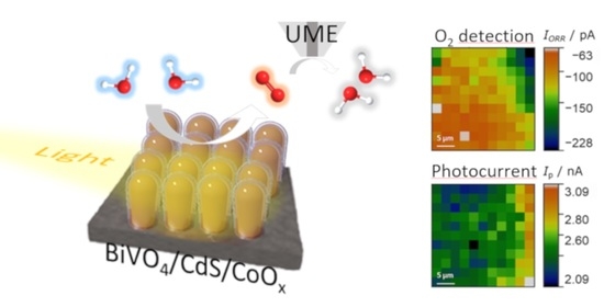
2.3. Scanning Photoelectrochemical Microscope Measurements

To investigate the local PEC activity of the designed photoanodes, SPECM measurements were carried out to locally detect the photocurrent and the O2 production from the reaction occurring at the sample. The SPECM setup is presented in Figure 6a. Acquisitions were made in a mode similar to the substrate generation—tip collection mode [48] (localized substrate photogeneration in our case) with synchronized light pulses, as presented in Figure 6b. This allows to measure the photocurrent from the sample and the oxygen reduction reaction (ORR) current at the microelectrode at each point of the scan. The currents during the last 10% of each light pulse were averaged, and the current values were transformed into a map at each wavelength and each position of the xy stage. The illumination time was chosen to reach a steady-state current during the averaged current calculation. A single measurement corresponding to one position of the xy stage is depicted in Figure 6c.
First, a large photocurrent map was recorded with an illumination spot of 100 µm at a wavelength of 340 nm (Figure 7a), and a high activity region was selected for further investigations.
The black cross indicates the spot for the subsequent SPECM experiments. The scans were performed in a constant-distance mode by shear-force sensing in a hopping mode.
Thanks to this constant-distance mode, the sample topography is obtained (see Figure 7b). This certifies the same probe-substrate distance at each matrix point and also corrects any contribution from the parallax between the probe and the substrate. A matrix scan allowed the subsequent detection of the photocurrent in the sample for two different wavelengths (340 and 387 nm, Figure 7c,d, respectively) and, simultaneously, the detection of the molecular O2 evolving from the substrate (i.e., the photoanode) by means of the ORR current recorded at the Pt microelectrode (Figure 7e,f, respectively). The microelectrode is biased to −0.6 V vs. Ag/AgCl to detect oxygen using the ORR. The maps show that high current areas in the photocurrent map are matched by low current areas in the ORR at the microelectrode (due to negative reduction current), indicating more active sites. Therefore, the higher photocurrent results in a higher local concentration of oxygen. Moreover, the maps at 387 nm show a slightly higher photocurrent and oxygen production compared to the ones at 340 nm. This is in agreement with the IPCE measurement on BiVO4/CdS/CoOx presented in Figure 5b. The overall shape of the photocurrent and ORR current maps for both wavelengths is equivalent.
This supposes no differences between both wavelengths in the local photoactivity of the photoanode. Photocurrent and ORR current maps were performed on BiVO4, BiVO4/CdS, and BiVO4/CoOx (see Figures S4–S6) nanostructured photoanodes. The same correlation of photocurrents and ORR currents was observed also for the BiVO4/CdS/CoOx sample.
Generally, some activity inhomogeneities are noticeable in the large photocurrent maps as well as in the small area scans. However, the roughness of the substrate is smaller than 1 µm in the investigated area (as shown Figure 7b), and the shear-force mode used during the investigation keeps the same probe-substrate distance all along. Thus, these current disparities are probably due to local composition inhomogeneities instead of topographical distribution. Furthermore, the topographical map presented in Figure 7b shows that thicker part of the scanned area corresponds to the highest activities measured in the photocurrent and ORR maps. This also suggests the presence of local inhomogeneities due to the local quantity of material or an incomplete surface modification from synthesis processes on the micro- or nanoscale.
As shown in the literature, SPECM allows to identify such local disparities [43]. This will be the focus of future works with quantitative studies using the same measurement method thoroughly explained in Figure S7.

2.4. Electrochemical Impedance Spectroscopy and Intensity Modulated Photocurrent Spectroscopy Measurements

Electrochemical impedance spectroscopy (EIS) was employed to examine the charge transport characteristics and photogenerated electron–hole separation efficiency. As depicted in Figure 8a, all plots show semicircles that are fitted by an appropriate 2-RC circuit (inset of Figure 8a) [33]. The fitted parameters are presented in Table 1.
A decrease in the charge transport resistance (RSC) and the charge transfer resistance (Rct) is observed upon formation of the composite of BiVO4 with CdS and CoOx. The RSC decreased by 45% for BiVO4/CdS. The same trend of RSC is further seen upon CoOx coating, which is about 60.3% in comparison with the pristine BiVO4. The decrease in RSC strongly supports that the enhanced electron–hole pair separation across the interfaces of BiVO4/CdS and CoOx is due to the built-in electric field upon heterojunction formation [33].
Furthermore, the hole transfer ability to the electrolyte, i.e., the catalytic properties of the photoanodes, is represented by Rct, and a significant change in the hole transfer ability upon CdS (decreased by ~60.6%) and CoOx (decreased by ~69.2%) coating compared to pristine BiVO4 is also observed. This emphasizes the efficient role of CdS and CoOx to improve the hole transfer ability across the photoanode/electrolyte interface [33]. This observation is also supported by the capacitance of the photoanode/electrolyte interface (CPE2). The CPE2 obtained for BiVO4/CdS/CoOx composite is approximately two times higher than the bare BiVO4, which strongly suggests the hole storage ability of the CoOx layer. Moreover, the hole storage ability of the CoOx layer improves the photostability of the material by limiting the photocorrosion process at the CdS shell [49]. Thus, this enhances the hole transfer rate across the photoanode/electrolyte interface via an efficient charge transfer across the multiple junctions of the composite photoanode system [33]. Hence, the BiVO4/CdS composite and its further modification with CoOx are effective to improve the charge transport/transfer characteristics compared to bare BiVO4 photoanode, thus improving the photocurrent while enabling better PEC stability.
To further characterize the electron transport properties, the intensity modulated photocurrent spectroscopy (IMPS) measurements were performed (Figure 8b). IMPS is a useful non-destructive technique for the determination of photogenerated charge carrier transit time (τd). The obtained τd for BiVO4/CdS and BiVO4/CdS/CoOx is 0.189 and 0.159 ms, respectively. These values are 15 and 18 times lower than those for bare BiVO4 (2.85 ms). This suggests a lower recombination probability of photogenerated electron–hole pairs for BiVO4/CdS and BiVO4/CdS/CoOx than bare BiVO4. Those values also demonstrate that the charge carriers reach the back contact of BiVO4/CdS and BiVO4/CdS/CoOx more readily without any significant recombination in comparison with pristine BiVO4. The observed faster transit time is mainly attributed to the efficient charge separation of the electron–hole pairs facilitated by the electric field developed across the interfaces of BiVO4/CdS and also BiVO4/CdS/CoOx. These results are in good agreement with the charge transport resistance values (RSC) obtained from the EIS measurements. The IMPS results further emphasize the significance of heterojunction and thus, the subsequent improvement in the charge transport/transfer characteristics as well as enhanced performance of BiVO4 composite photoanodes.

3. Experimental

3.1. Materials

All chemicals and solvents were purchased in the highest purity from Sigma Aldrich (Prague, Czech Republic) and used as received. The purity of each chemical is specified below in the description of experimental procedures.

3.2. BiVO4 Photoanodes Preparation

The BiVO4 photoanodes were prepared via a two-step synthetic procedure. First, BiOI films were synthesized by electrodeposition, and they served as a precursor to form BiVO4 electrodes. The plating solution was an aqueous solution of 400 mM potassium iodide (KI (>99%)) and 40 mM bismuth nitrate pentahydrate (Bi (NO3)3·5H2O (99.99%)). The pH of the solution was adjusted to 1.8 by adding nitric acid (HNO3 (70%)). Then, the ethanol solution containing 46 mM p-benzoquinone (>98%) was slowly added. The final pH of the mixed solution was adjusted to 3.4 by adding HNO3. The potentiostatic deposition was performed in a typical three-electrode electrochemical cell. The mechanism and condition for BiOI electrodeposition by the reduction of p-benzoquinone to hydroquinone were reported previously [49]. Herein, a fluorine-doped tin oxide glass substrate (hereafter FTO) was the working electrode (WE), platinum wire was the counter electrode (CE), and Ag/AgCl (3 M KCl) served as the reference electrode (RE). A continuous potential of −0.2 V vs. Ag/AgCl was applied for about 360 s. Then, the substrate was cleaned with distilled water and dried with an air stream.
Second, the BiOI film was converted to BiVO4 by chemical and thermal treatments. The surface of BiOI was covered by drop-casting 150 µL of a dimethyl sulfoxide (>99.9%) solution containing 200 mM of vanadyl acetylacetonate (VO (acac)2 (98%)). Then, the film was annealed in air at 450 °C for 2 h (5 °C/min). The obtained BiVO4 electrode was soaked in 1 M sodium hydroxide (NaOH (>99.98%)) for 30 min under stirring in order to remove the excess of V2O5. Finally, the resulting electrode was thoroughly rinsed with distilled water and dried with an air stream.

3.3. Preparation of BiVO4/CdS and BiVO4/CdS/CoOx Heterostructures

For the deposition of the CdS film, 2 mM cadmium nitrate (Cd(NO3)2 (99.99%)) and 10 mM thiourea (>99%) solutions were prepared. Then, the aqueous ammonia (25 wt. %, >99.98%) was added which was used as a complexing agent. The CdS film was then deposited by dipping the FTO glass into the precursor solution at 85 °C for 90 min. The substrate was then rinsed with distilled water and dried with an air stream.
Finally, the CoOx co-catalyst was electrodeposited on the top of BiVO4/CdS from an aqueous solution containing 0.1 M of cobalt nitrate hexahydrate (Co(NO3)2·6H2O (98%)), adjusted at pH = 7, by applying a potential of −0.2 V vs. Ag/AgCl for 240 s. Then, the sample was rinsed with distilled water and air dried.

3.4. Photoelectrochemical Measurements

The PEC experiments were carried out in an electrochemical cell with a typical three-electrode arrangement. Such prepared photoanodes served as the WE, the Ag/AgCl in 3 M KCl was used as the RE, and the Pt wire was used as the CE. The photoanodes were illuminated by a 150 W xenon lamp coupled with AM 1.5 G filter with the standard power intensity of 1 sun (i.e., 100 mW cm−2). A 0.1 M sodium sulfite (Na2SO3 (98%)) or sodium sulfate (Na2SO4 (>99%)) potassium buffer solution served as the electrolyte. The Gamry Series G 300 Potentiostat was used for PEC measurements. The PEC behavior of the prepared electrodes was investigated by means of LSV measurements and IPCE. Each type of photoanode was fabricated and tested at least three times, and the representative curves are reported.
Applied potentials were converted to the RHE by the following equation:
E R H E = E A g / A g C l + E A g / A g C l 0 + 0.059 × p H .
In our case, E A g / A g C l 0 = 0.1976 V at 25 °C was the standard potential of Ag/AgCl reference electrode.
The latter was measured with a 300 W xenon lamp coupling with an aligned monochromator Oriel TLS−300 X (Newport, Irvine, CA, USA). The IPCE was calculated according to the following equation:
I P C E = J S C P i n × 1240 λ × 100 % ,
where Jsc is photocurrent density (mA cm−2) measured at 0.6 V vs. RHE under single wavelength (λ) and Pin is the irradiance intensity (mW cm−2) of the monochromatic light.
EIS of the samples was measured by applying a bias and in a frequency ranging from 0.05 Hz to 1 MHz under simulated sunlight conditions.
IMPS measurements were performed using a Zahner PP 211 CIMPS setup (ZAHNER-elektrik GmbH, Kronach, Germany) with a light diode (λ = 510 nm) in a frequency range of 0.1 Hz to 105 Hz with a fixed light intensity of 100 mW cm−2. A sinusoidal perturbation of ~10% of the steady-state illumination was used for the superimposition. The time taken by the charge carrier to reach the back contact of the photoanode, called transit time (τd), can be estimated from the equation:
τ d = 1 2 π f m i n   ( I M P S ) ,
where fmin represents the minimum frequency value of the IMPS plot.

3.5. Scanning Photoelectrochemical Microscopy Measurements

SPECM experiments were conducted using an ELP 3 SPECM-FL (HEKA Elektronik GmbH, Lambrecht, Germany), a PG 618 USB bipotentiostat (HEKA Elektronik GmbH, Lambrecht, Germany), and a Lambda DG−4 illumination system (Sutter Instrument, Novato, CA, USA) with bandpass filters for 340 and 387 nm (Thorlabs GmbH, Bergkirchen, Germany). This technique was already proved as a powerful tool to locally investigate PEC reactions [48,50].
The experiments were performed in 0.1 M Na2SO3 in phosphate buffer (pH 7). A Pt microelectrode (r = 5 µm, HEKA Elektronik GmbH, Lambrecht, Germany) was employed as WE2, the sample was electrically connected as WE1, an Ag/AgCl wire was used as RE, and a Pt wire served as counter electrode, CE. The sample was biased to +0.2 V vs. Ag/AgCl. A potential of −0.6 V vs. Ag/AgCl was applied to the Pt microelectrode. The light beam (r = 2.5 µm) and the microelectrode were aligned (See Figure S1), and the sample was scanned on the xy stage. Shear-force sensing was employed for constant-distance scans. Therefore, the microelectrode was approached to and retracted from the surface by 5 µm under shear-force control. A topography map was extracted from the z-piezo value at the end point of the shear-force controlled approach. The experiments were conducted in a matrix scan.

3.6. Physical Characterization

The surface morphology images were captured by a SEM Hitachi SU6600 with an accelerating voltage of 15 kV. Elemental mapping was obtained using a HR-TEM TITAN operating at 80 kV. EDS measurements were done with an acquisition time of 20 min. UV–VIS diffuse reflectance absorption spectra were collected on a FLS980 fluorescence spectrometer (Edinburgh Instruments, Livingston, United Kingdom) equipped with an integrating sphere with its inner face coated with BENFLEC. The standard BENFLEC plate was used as reflectance standard. GIXRD patterns of the samples were collected using an empyrean diffractometer (PANalytical) equipped with a focusing X-ray mirror for Co radiation, 3-axis cradle, a multichannel detector PIXcel3D (1D mode), and Co-Kα radiation (40 kV, 30 mA, λ = 0.1789 nm). The measurement range used was 2θ = 15°–80°, along with a step size of 0.052° and variable incidence angle of ω = 4°, 2°, and 1°. XPS measurements were conducted using a PHI VersaProbe II (Physical Electronics, Chanhassen, MN, USA) spectrometer with Al Kα source (15 kV, 50 W). The spectra were measured in vacuum at room temperature and were evaluated with MultiPak (ULVAC-PHI, Inc., Kanagawa, Japan) software.

4. Conclusions

In summary, we demonstrated a facile approach to fabricate BiVO4/CdS/CoOx nano-assembly heterojunctions. We achieved an efficient tri-component PEC system by a simple electrochemical and thermal treatment and chemical bath deposition techniques. The BiVO4/CdS heterostructure demonstrated a significant shift in the band edge, which facilitated effective visible light absorption. In addition, to improve the stability of BiVO4/CdS core–shell structure, we coated it with a CoOx overlayer. The resultant BiVO4/CdS/CoOx multi-component system yielded a significant higher photocurrent (4.93 mA cm−2 at 1.1 V vs. RHE) in comparison with pristine CdS (1.19 mA cm−2 at 1.1 V vs. RHE) and BiVO4 (2.1 mA cm−2 at 1.1 V vs. RHE). The CoOx layer enhanced the stability of the material by limiting the photocorrosion of the CdS shell. The photocurrent was locally compared with the O2 production thanks to the SPECM technique. This showed a similar trend in every measurement between the photocurrent and the O2 production and confirmed that the water oxidation reaction occurred at the sample. The local studies showed photocurrent/O2 detection inhomogeneities suggesting that even for such a photoactive material, there is room for improvement. We carried out electrochemical EIS and IMPS measurements to demonstrate the charge transport/transfer ability of such a multi-component system to enhance the photocurrent and efficiency in water oxidation. Overall, it was shown that the precise design of core–shell multi-component PEC systems including diverse light absorbers and protective overlayer is an effective strategy to achieve highly performing photoanodes with superior PEC stability.

Supplementary Materials

The following are available online at https://www.mdpi.com/article/10.3390/catal11060682/s1, Figure S1: Optical image with the inverse microscope of the alignment of microelectrode and illumination spot. rspot = 2.5 µm, rT = 5 µm and RG = 5.7., Figure S2: XPS survey of BiVO4/CdS photoanode., Figure S3: LSV scans under AM 1.5G illumination with (Na2SO3) and without (Na2SO4) hole scavenger for bare BiVO4, BiVO4/CdS, BiVO4/CoOx and BiVO4/CdS/CoOx photoanodes., Figure S4: Photocurrent (a) and ORR current maps at the microelectrode (b) at 340 nm on a 50 × 50 µm² matrix map at bare BiVO4., Figure S5: Photocurrent (a) and ORR current maps at the microelectrode (b) at 340 nm on a 100 × 75 µm² matrix map at BiVO4/CdS photoanode., Figure S6: Photocurrent (a) and ORR current maps at the microelectrode (b) at 340 nm on a 100 × 50 µm² matrix map at BiVO4/CoOx photoanode., Figure S7. Example of a simultaneous measurement at one point of the matrix, showing the photocurrent at the substrate (sample) and the ORR current at the probe (microelectrode) upon illumination of the sample for 340 and 387 nm with a 2 s delay between the on/off light switch. The light delay is decided to obtain a steady-state at the baseline and signal acquisition parts (green and red areas, respectively). The baseline is subtracted to the signal acquired to obtain the photoactivity induced during the measurement both at the substrate (from the measured photocurrent) and the probe (from the ORR measured current).

Author Contributions

H.K.: conceptualization, data curation, and investigation, writing—original draft. O.H.: formal analysis, software, writing—original draft, writing—review and editing, and visualization. R.Y.: data curation, methodology, and validation. M.H.: data curation and investigation. C.H.: methodology and validation. R.Z.: validation and resources. P.S.: validation and funding acquisition. A.N.: validation, resources, writing—review and editing, and supervision. Š.K.: conceptualization and supervision. All authors have read and agreed to the published version of the manuscript.

Funding

This research was funded by the Operational Programme Research, Development and Education—European Regional Development Fund, project no. CZ.02.1.01/0.0/0.0/15_003/0000416 of the Ministry of Education, Youth and Sports of the Czech Republic.

Conflicts of Interest

The authors declare that they have no known competing financial interests or personal relationships that could have appeared to influence the work reported in this paper.

References

  1. Hisatomi, T.; Kubota, J.; Domen, K. Recent advances in semiconductors for photocatalytic and photoelectrochemical water splitting. Chem. Soc. Rev. 2014, 43, 7520–7535. [Google Scholar] [CrossRef]
  2. Gibson, T.L.; Kelly, N.A. Optimization of solar powered hydrogen production using photovoltaic electrolysis devices. Int. J. Hydrogen Energy 2008, 33, 5931–5940. [Google Scholar] [CrossRef]
  3. Chen, X.; Shen, S.; Guo, L.; Mao, S.S. Semiconductor-based photocatalytic hydrogen generation. Chem. Rev. 2010, 110, 6503–6570. [Google Scholar] [CrossRef]
  4. Walter, M.G.; Warren, E.L.; McKone, J.R.; Boettcher, S.W.; Mi, Q.; Santori, E.A.; Lewis, N.S. Solar water splitting cells. Chem. Rev. 2010, 110, 6446–6473. [Google Scholar] [CrossRef]
  5. Hoffmann, M.R.; Martin, S.T.; Choi, W.; Bahnemann, D.W. Environmental applications of semiconductor photocatalysis. Chem. Rev. 1995, 95, 69–96. [Google Scholar] [CrossRef]
  6. Sivula, K.; van de Krol, R. Semiconducting materials for photoelectrochemical energy conversion. Nat. Rev. Mater. 2016, 1, 1–16. [Google Scholar] [CrossRef]
  7. Ros, C.; Andreu, T.; Morante, J.R. Photoelectrochemical water splitting: A road from stable metal oxides to protected thin film solar cells. J. Mater. Chem. A. 2020, 8, 10625–10669. [Google Scholar] [CrossRef]
  8. Kim, J.H.; Lee, J.S. BiVO4-Based Heterostructured photocatalysts for solar water splitting: A review. Energy Environ. Focus 2014, 3, 339–353. [Google Scholar] [CrossRef]
  9. Yalavarthi, R.; Zbořil, R.; Schmuki, P.; Naldoni, A.; Kment, Š. Elucidating the role of surface states of BiVO4 with Mo doping and a CoOOH co-catalyst for photoelectrochemical water splitting. J. Power Sources 2021, 483, 229080. [Google Scholar] [CrossRef]
  10. Kudo, A.; Ueda, K.; Kato, H.; Mikami, I. Photocatalytic O2 evolution under visible light irradiation on BiVO4 in aqueous AgNO3 solution. Catal. Lett. 1998, 53, 229–230. [Google Scholar] [CrossRef]
  11. Kim, J.H.; Jang, J.-W.; Jo, Y.H.; Abdi, F.F.; Lee, Y.H.; van de Krol, R.; Lee, J.S. Hetero-type dual photoanodes for unbiased solar water splitting with extended light harvesting. Nat. Commun. 2016, 7, 13380. [Google Scholar] [CrossRef] [Green Version]
  12. Liang, Y.; Tsubota, T.; Mooij, L.P.A.; van de Krol, R. Highly improved quantum efficiencies for thin film BiVO4 photoanodes. J. Phys. Chem. C 2011, 115, 17594–17598. [Google Scholar] [CrossRef]
  13. Friedrich, D.; Kressman, S.; Strub, H.; Artero, V.; Laberty-Robert, C.; Hillard, S. Solar-water-splitting BiVO4 thin-film photoanodes prepared by using a sol–gel dip-coating technique. ChemPhotoChem 2017, 1, 273–280. [Google Scholar] [CrossRef]
  14. Chen, L.; Alarcón-Lladó, E.; Hettick, M.; Sharp, I.D.; Lin, Y.; Javey, A.; Ager, J.W. Reactive sputtering of bismuth vanadate photoanodes for solar water splitting. J. Phys. Chem. C 2013, 117, 21635–21642. [Google Scholar] [CrossRef] [Green Version]
  15. Murcia-López, S.; Fàbrega, C.; Monllor-Satoca, D.; Hernández-Alonso, M.D.; Penelas-Pérez, G.; Morata, A.; Morante, J.R.; Andreu, T. Tailoring multilayered BiVO4 photoanodes by pulsed laser deposition for water splitting. ACS Appl. Mater. Inter. 2016, 8, 4076–4085. [Google Scholar] [CrossRef] [PubMed]
  16. Kölbach, M.; Harbauer, K.; Ellmer, K. Elucidating the pulsed laser deposition process of BiVO4 photoelectrodes for solar water splitting. J. Phys. Chem. C 2020, 124, 4438–4447. [Google Scholar] [CrossRef]
  17. Sayama, K.; Nomura, A.; Arai, T.; Sugita, T.; Abe, R.; Yanagida, M.; Oi, T.; Iwasaki, Y.; Abe, Y.; Sugihara, H. Photoelectrochemical decomposition of water into H2 and O2 on porous BiVO4 thin-film electrodes under visible light and significant effect of Ag ion treatment. J. Phys. Chem. B 2006, 110, 11352–11360. [Google Scholar] [CrossRef] [PubMed]
  18. Luo, H.; Mueller, A.H.; McCleskey, T.M.; Burrell, A.K.; Bauer, E.; Jia, Q.X. Structural and photoelectrochemical properties of BiVO4 thin-films. J. Phys. Chem. C 2008, 112, 6099–6102. [Google Scholar] [CrossRef]
  19. Kim, T.W.; Choi, K.-S. Nanoporous BiVO4 photoanodes with dual-layer oxygen evolution catalysts for solar water splitting. Science 2014, 343, 990–994. [Google Scholar] [CrossRef]
  20. Park, Y.; McDonald, K.J.; Choi, K.-S. Progress in bismuth vanadate photoanodes for use in solar water oxidation. Chem. Soc. Rev. 2013, 42, 2321–2337. [Google Scholar] [CrossRef]
  21. Li, R.; Zhang, F.; Wang, D.; Yang, J.; Li, M.; Zhu, J.; Zhou, X.; Han, H.; Li, C. Spatial separation of photogenerated electrons and holes among {010} and {110} crystal facets of BiVO4. Nat. Commun. 2013, 4, 1432. [Google Scholar] [CrossRef] [Green Version]
  22. Zhang, B.; Chou, L.; Bi, Y. Tuning surface electronegativity of BiVO4 photoanodes toward highperformance water splitting. Appl. Catal. B Environ. 2020, 262, 118267. [Google Scholar] [CrossRef]
  23. Seabold, J.A.; Zhu, K.; Neale, N.R. Efficient solar photoelectrolysis by nanoporous Mo:BiVO4 through controlled electron transport. Phys. Chem. Chem. Phys. 2013, 16, 1121–1131. [Google Scholar] [CrossRef]
  24. Jua, S.; Seokb, H.-J.; Juna, J.; Huha, D.; Sona, S.; Kima, K.; Kima, W.; Baeka, S.; Kimb, H.-K.; Leea, H. Fully blossomed WO3/BiVO4 structure obtained via active facet engineering of patterned FTO for highly efficient water splitting. Appl. Catal. B Environ. 2020, 263, 118362. [Google Scholar] [CrossRef]
  25. She, H.; Yue, P.; Ma, X.; Huang, J.; Wang, L.; Wang, Q. Fabrication of BiVO4 photoanode cocatalyzed with NiCo-layered double hydroxide for enhanced photoactivity of water oxidation. Appl. Catal. B Environ. 2020, 263, 118280. [Google Scholar] [CrossRef]
  26. Zhou, S.; Chen, K.; Huang, J.; Wang, L.; Zhang, M.; Bai, B.; Liu, H.; Wang, Q. Preparation of heterometallic CoNi-MOFs-modified BiVO4: A steady photoanode for improved performance in photoelectrochemical water splitting. Appl. Catal. B Environ. 2020, 266, 118513. [Google Scholar] [CrossRef]
  27. Zhong, M.; Hisatomi, T.; Kuang, Y.; Zhao, J.; Liu, M.; Iwase, A.; Jia, Q.; Nishiyama, H.; Minegishi, T.; Nakabayashi, M.; et al. Surface modification of CoOx loaded BiVO4 photoanodes with ultrathin p-Type NiO layers for improved solar water oxidation. J. Am. Chem. Soc. 2015, 137, 5053–5060. [Google Scholar] [CrossRef] [PubMed]
  28. Sun, Q.; Cheng, T.; Liu, Z.; Qi, L. A cobalt silicate modified BiVO4 photoanode for efficient solar water oxidation. Appl. Catal. B-Environ. 2020, 277, 119189. [Google Scholar] [CrossRef]
  29. Zhong, D.K.; Choi, S.; Gamelin, D.R. Near-Complete Suppression of surface recombination in solar photoelectrolysis by “Co-Pi” catalyst-modified W:BiVO4. J. Am. Chem. Soc. 2011, 133, 18370–18377. [Google Scholar] [CrossRef]
  30. Shi, X.; Choi, I.Y.; Zhang, K.; Kwon, J.; Kim, D.Y.; Lee, J.K.; Oh, S.H.; Kim, J.K.; Park, J.H. Efficient photoelectrochemical hydrogen production from bismuth vanadate-decorated tungsten trioxide helix nanostructures. Nat. Commun. 2014, 5, 4775. [Google Scholar] [CrossRef] [PubMed] [Green Version]
  31. Kment, Š.; Sivula, K.; Naldoni, A.; Sarmah, S.P.; Kmentová, H.; Kulkarni, M.; Rambabu, Y.; Schmuki, P.; Zbořil, R. FeO-based nanostructures and nanohybrids for photoelectrochemical water splitting. Prog. Mater. Sci. 2020, 110, 100632. [Google Scholar] [CrossRef]
  32. Li, H.; Xia, Z.; Chen, J.; Lei, L.; Xing, J. Constructing ternary CdS/reduced graphene oxide/TiO2 nanotube arrays hybrids for enhanced visible-light-driven photoelectrochemical and photocatalytic activity. Appl. Catal. B Environ. 2015, 168–169, 105–113. [Google Scholar] [CrossRef]
  33. Rambabu, Y.; Dhua, S.; Jaiswal, M.; Roy, S.C. High photoelectrochemical performance of reduced graphene oxide wrapped, CdS functionalized, TiO2 multi-leg nanotubes. Nanotechnology 2020, 31, 275701. [Google Scholar] [CrossRef] [PubMed]
  34. Pareek, A.; Gopalakrishnan, A.; Borse, P.H. Efficiency and stability aspects of CdS photoanode for solar hydrogen generation technology. J. Phys. Conf. Ser. 2016, 755, 012006. [Google Scholar] [CrossRef]
  35. Kudo, A.; Miseki, Y. Heterogeneous photocatalyst materials for water splitting. Chem. Soc. Rev. 2008, 38, 253–278. [Google Scholar] [CrossRef]
  36. Han, B.; Liu, S.; Xu, Y.-J.; Tang, Z.-R. 1D CdS nanowire–2D BiVO4 nanosheet heterostructures toward photocatalytic selective fine-chemical synthesis. RSC Adv. 2015, 5, 16476–16483. [Google Scholar] [CrossRef]
  37. Ye, F.; Li, H.; Yu, H.; Chen, S.; Quan, X. Constructing BiVO4-Au@CdS photocatalyst with energic charge-carrier-separation capacity derived from facet induction and Z-scheme bridge for degradation of organic pollutants. Appl. Catal. B Environ. 2018, 227, 258–265. [Google Scholar] [CrossRef]
  38. Zhou, F.Q.; Fan, J.C.; Xu, Q.J.; Min, Y.L. BiVO4 nanowires decorated with CdS nanoparticles as Z-scheme photocatalyst with enhanced H2 generation. Appl. Catal. B Environ. 2017, 201, 77–83. [Google Scholar] [CrossRef]
  39. Wu, X.; Zhao, J.; Wang, L.; Han, M.; Zhang, M.; Wang, H.; Huang, H.; Liu, Y.; Kang, Z. Carbon dots as solid-state electron mediator for BiVO4/CDs/CdS Z-scheme photocatalyst working under visible light. Appl. Catal. B Environ. 2017, 206, 501–509. [Google Scholar] [CrossRef]
  40. Bao, S.; Wu, Q.; Chang, S.; Tian, B.; Zhang, J. Z-scheme CdS–Au–BiVO4 with enhanced photocatalytic activity for organic contaminant decomposition. Catal. Sci. Technol. 2017, 7, 124–132. [Google Scholar] [CrossRef]
  41. Meissner, D.; Memming, R.; Kastening, B.; Bahnemann, D. Fundamental problems of water splitting at cadmium sulfide. Chem. Phys. Lett. 1986, 127, 419–423. [Google Scholar] [CrossRef]
  42. Hou, J.; Wang, Z.; Yang, C.; Cheng, H.; Jiao, S.; Zhu, H. Cobalt-bilayer catalyst decorated Ta3N5 nanorod arrays as integrated electrodes for photoelectrochemical water oxidation. Energy Environ. Sci. 2013, 6, 3322–3330. [Google Scholar] [CrossRef]
  43. Yalavarthi, R.; Henrotte, O.; Minguzzi, A.; Ghigna, P.; Grave, D.A.; Naldoni, A. In situ characterizations of photoelectrochemical cells for solar fuels and chemicals. MRS Energy Sustain. 2020, 7. [Google Scholar] [CrossRef]
  44. Moniruddin, M.; Oppong, E.; Stewart, D.; McCleese, C.; Roy, A.; Warzywoda, J.; Nuraje, N. Designing CdS-based ternary heterostructures consisting of Co-metal and CoOx cocatalysts for photocatalytic H2 evolution under visible light. Inorg. Chem. 2019, 58, 12325–12333. [Google Scholar] [CrossRef]
  45. Jina, S.; Maa, X.; Pana, J.; Zhub, C.; Sajic, S.E.; Hua, J.; Xua, X.; Sunb, L.; Yinc, Z. Oxygen vacancies activating surface reactivity to favor charge separation and transfer in nanoporous BiVO4 photoanodes. Appl. Catal. B Environ. 2021, 281, 119477. [Google Scholar] [CrossRef]
  46. Liu, Y.; Ding, S.; Shi, Y.; Liu, X.; Wu, Z.; Jiang, Q.; Zhou, T.; Liu, N.; Hu, J. Construction of CdS/CoOx core-shell nanorods for efficient photocatalytic H2 evolution. Appl. Catal. B Environ. 2018, 234, 109–116. [Google Scholar] [CrossRef]
  47. Son, J.S.; Lee, J.-S.; Shevchenko, E.V.; Talapin, D.V. Magnet-in-the-semiconductor nanomaterials: High electron Mobility in all-inorganic arrays of FePt/CdSe and FePt/CdS core–shell heterostructures. J. Phys. Chem. Lett. 2013, 4, 1918–1923. [Google Scholar] [CrossRef]
  48. James, P.; Casillas, N.; Smyrl, W.H. Simultaneous scanning electrochemical and photoelectrochemical microscopy by use of a metallized optical fiber. J. Electrochem. Soc. 1996, 143, 3853. [Google Scholar] [CrossRef]
  49. Govindaraju, G.V.; Wheeler, G.P.; Lee, D.; Choi, K.-S. Methods for electrochemical synthesis and photoelectrochemical characterization for photoelectrodes. Chem. Mater. 2017, 29, 355–370. [Google Scholar] [CrossRef]
  50. Zhao, F.; Plumeré, N.; Nowaczyk, M.M.; Ruff, A.; Schuhmann, W.; Conzuelo, F. Interrogation of a PS1-Based Photocathode by Means of scanning photoelectrochemical microscopy. Small 2017, 13, 1604093. [Google Scholar] [CrossRef]
Figure 1. Schematic illustration of the fabrication process employed to prepare different photoanodes, namely, BiVO4, BiVO4/CdS, and BiVO4/CdS/CoOx.
Catalysts 11 00682 g001
Figure 2. (a) XRD patterns of FTO, BiVO4, CdS, BiVO4/CdS, and BiVO4/CdS/CoOx films. (b) Normalized UV–VIS diffuse reflectance spectra of BiVO4, CdS, BiVO4/CdS, and BiVO4/CdS/CoOx photoanodes.
Catalysts 11 00682 g002
Figure 3. SEM images of (a) BiOI, (b) BiVO4, and (c) BiVO4/CdS composites; (d) high-angle annular dark-field (HAADF) image, and (ek) EDS elemental mapping of Bi, V, Cd, Co, joined Bi-V-Co, and Bi-Co-Cd taken for the BiVO4/CdS/CoOx heterostructure; (l,m) HR-TEM images and (n) selected area electron diffraction pattern (SAED) of such a BiVO4/CdS/CoOx photoanode. The 200 nm scalebar is the same from the images d to k.
Catalysts 11 00682 g003
Figure 4. XPS spectra of the as-prepared photoanodes: (a) Bi 4f, (b) V 2p, (c) O 1s (from BiVO4), (d) Cd 3d, (e) S 2p, (f) O 1s (from BiVO4/CdS), (g) Co 2p, and (h) O 1s (from BiVO4/CdS/CoOx) and (i) survey of BiVO4/CdS/CoOx.
Catalysts 11 00682 g004
Figure 5. (a) LSV scans under AM 1.5G illumination of the bare BiVO4, bare CdS, BiVO4/CdS, BiVO4/CoOx, and BiVO4/CdS/CoOx photoanodes. (b) IPCE spectra of the BiVO4, BiVO4/CdS, and BiVO4/CdS/CoOx photoanodes. (c) Photostability test of the as-prepared BiVO4/CdS/CoOx photoanode by chronoamperometry at 1.1 V vs. RHE for 135 min under AM 1.5G illumination.
Catalysts 11 00682 g005
Figure 6. (a) Schematic presentation of the SPECM setup used for the SPECM measurements. (b) Schematic presentation of the substrate generation—tip collection mode in the case of water oxidation at a BiVO4/CdS/CoOx photoanode under illumination. (c) Schematic presentation of a simultaneous measurement at one point of the matrix, showing the photocurrent at the substrate (sample) and the ORR current at the probe (microelectrode) upon illumination of the sample for 340 and 387 nm with a 2 s delay between the on/off light switch.
Catalysts 11 00682 g006
Figure 7. (a) A large photocurrent map with an illumination (λ = 340 nm) spot size of r = 50 µm was obtained as an overview. Simultaneous measurements with a small spot illumination (r = 2.5 µm) were performed yielding images of the topography via shear force sensing (b), the photocurrent at the sample at 340 nm (c) and 387 nm (d) and ORR current at the microelectrode (rT = 5 µm) at 340 nm (e) and 387 nm (f).
Catalysts 11 00682 g007
Figure 8. (a) Nyquist plots of EIS measured under AM 1.5G at 100 mW cm−2 (symbols) and fitting curves (line) and (b) the intensity-modulated photocurrent spectroscopy plots of the normalized efficiency vs. log (frequency) of the as-prepared photoanodes.
Catalysts 11 00682 g008
Table 1. Electrical parameters extracted by fitting EIS data with the equivalent circuit shown in Figure 8a for BiVO4, BiVO4/CdS, and BiVO4/CdS/CoOx. Rs is the resistance of the solution, RSC is the resistance of the space charged layer (or to charge transport), and Rct is the resistance to charge transfer at the photoanode/electrolyte interface.
SampleRS (Ω)RSC (Ω)Rct (Ω)CPE2 (µF)
BiVO424.43 ± 1.2116 ± 14992 ± 1587.9 ± 0.8
BiVO4/CdS19.07 ± 1.664 ± 17390 ± 12170 ± 1.9
BiVO4/CdS/CoOx12.61 ± 0.746 ± 2305 ± 6203 ± 1.6
Publisher’s Note: MDPI stays neutral with regard to jurisdictional claims in published maps and institutional affiliations.

