1. Introduction
Electric vehicles, cloud technology, and artificial intelligence are emerging industries whose development is hindered by power requirements. In particular, electric vehicles are more efficient at converting power from their power plant to vehicular motion relative to conventional combustion-engine vehicles—where the conversion efficiency of an electric vehicle is determined both by the motor and the overall power conversion system. In addition, cloud technology will become increasingly important as remote work becomes the norm. Powerful servers and high-power systems are required to handle large volumes of data being transmitted in and out of the cloud. These developments necessitate the design of a compact, high-conversion-efficiency, and high-power system [
1].
DC/DC converters are either isolated or non-isolated depending on whether the converter has a transformer. Common non-isolated converters include the buck converter, boost converter, and buck-boost converter. These converters have simpler topologies and thus simpler circuitry; however, they cannot achieve high conversion efficiency when the step-down ratio is high due to the lack of a transformer and also cannot provide electrical isolation. Non-isolated DC/DC converters are more commonly found in buck-boost applications at the back end of isolated converters.
Common isolated converters include the flyback converter, half-bridge converter, and full-bridge converter. Isolated converters have transformers and therefore feature high step-down ratios and electrical isolation capability [
2,
3,
4,
5,
6,
7]. Flyback converters have simple structures and can be constructed with a few components; because these converters have only one power transistor, the voltage stress is rather high, and flyback converters are thus typically low-power converters. Half-bridge converters have one more power transistor than flyback converters and consequently lower voltage stress. Because the transformer inputs are half-wave signals, the operating current of the power transistor is higher than that of flyback converters. In applications with high input voltages and high power, choosing an appropriate power transistor is critical. Relative to half-bridge converters, full-bridge converters have two more power transistors, which reduce voltage stress, and use full-wave signals as transistor inputs, which further reduce the operating current of the power transistors while increasing control complexity. These converters are primarily used in high-voltage and high-power applications [
8,
9,
10].
The LLC resonant converter selected in this study can be employed in both half-bridge and full-bridge architectures and uses pulse frequency modulation to maintain the duty cycle of the transistor at approximately 50% by modulating the driving signal to modulate the power output. The LLC resonant converter also has the following features [
11,
12,
13]:
In any state, the primary-side power transistor of the converter remains in the ZVS state; in a fully loaded state, the secondary-side rectifier enters the zero current switching state;
When fully loaded, the switching frequency of the converter will be equal to the resonant frequency, improving its performance;
The cutoff switching current of the power transistor can be lowered by increasing , thus reducing switching loss;
and can be integrated or isolated. Integrating the two can effectively reduce the size of the converter and save on costs, whereas isolating the two enables the precise control of the resonant inductance value and enhances converter efficiency.
Table 1 presents the basic characteristics of an LLC resonant transformer when used in a half-bridge converter or a full-bridge converter.
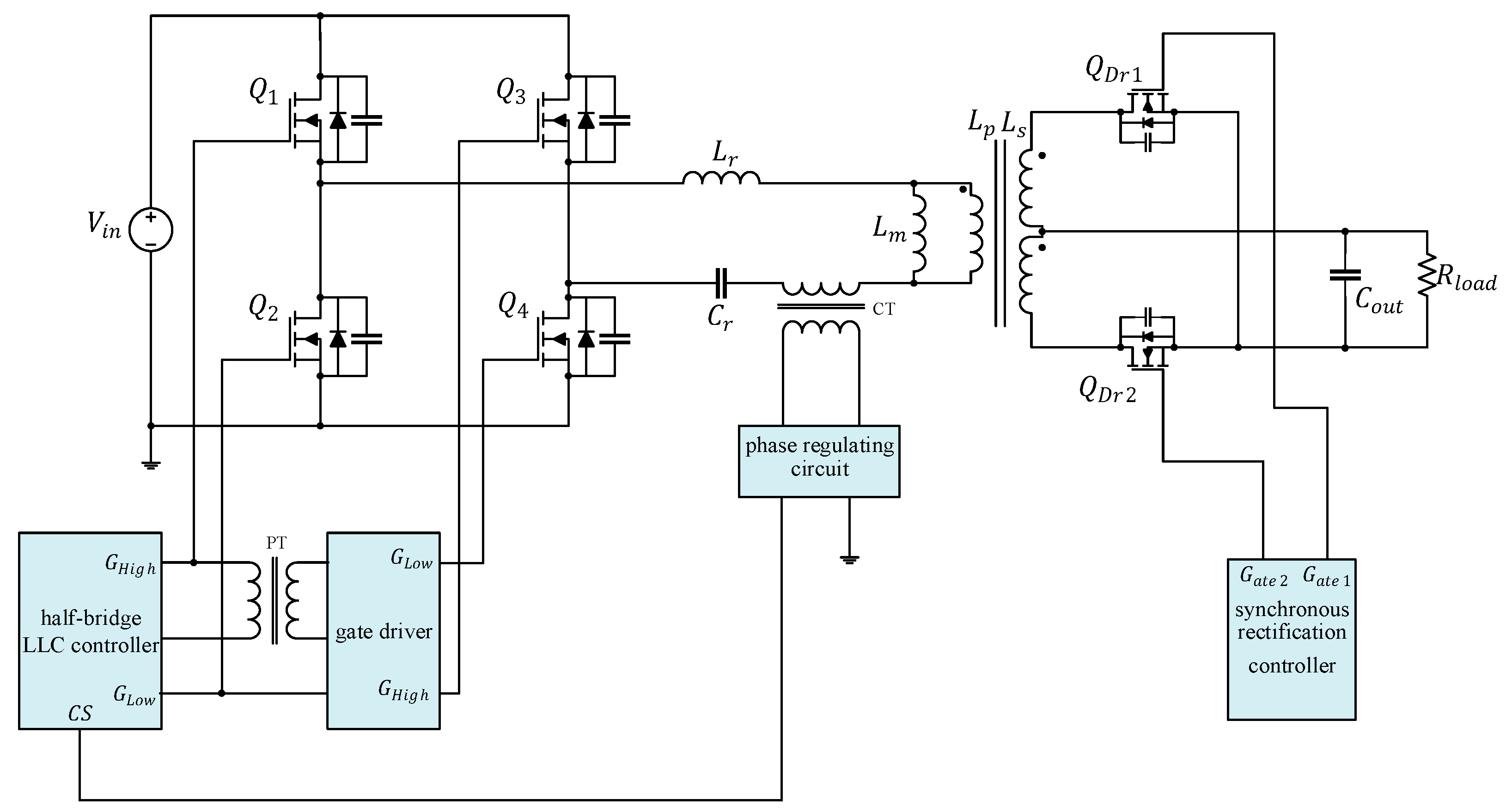
The full-bridge architecture is generally used in high-power and high-efficiency converters. However, given the lack of commercially available control chips for full-bridge LLC converters, in this paper, a full-bridge LLC resonant converter was fabricated using a half-bridge LLC resonant control chip. In order to maintain full-bridge power transistors in the ZVS states with a half-bridge LLC resonant control chip, the output parasitic capacitance of the first-arm power transistors was determined so that they can be added appropriately to improve the converter efficiency.
2. Operating Principles
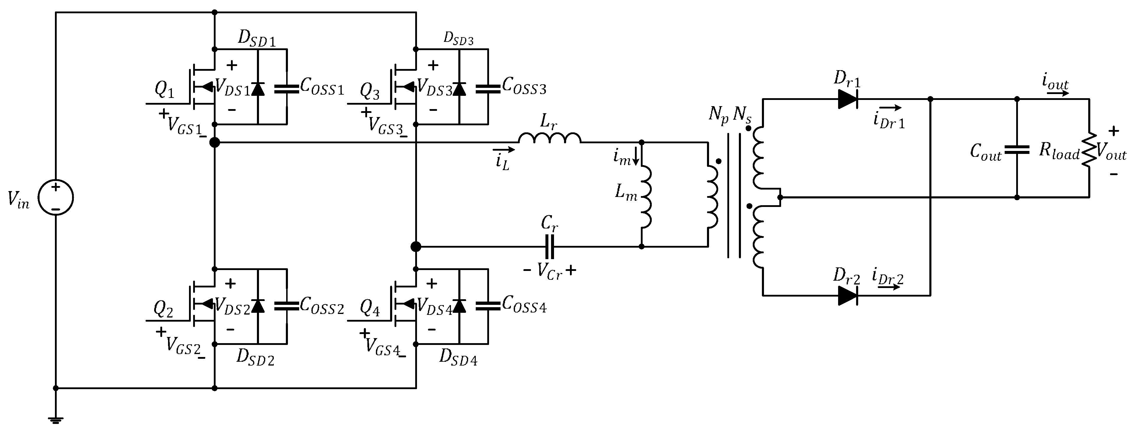
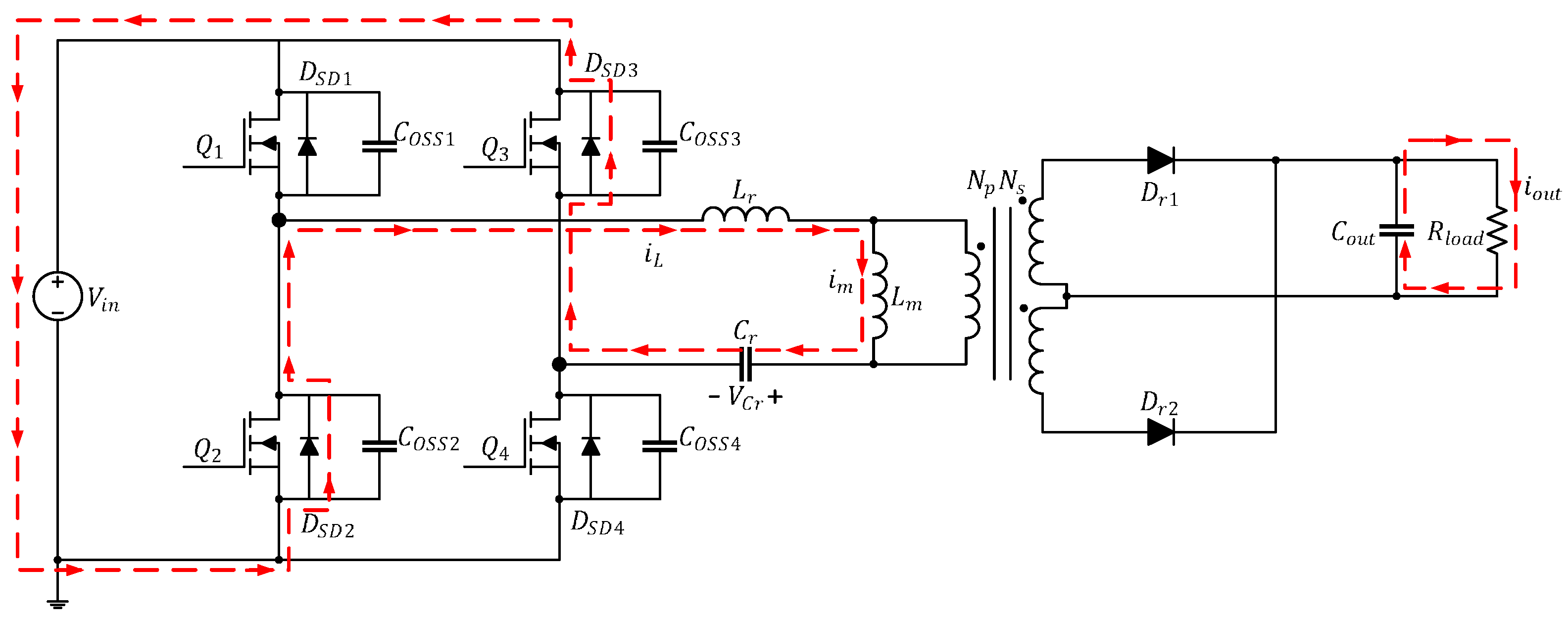
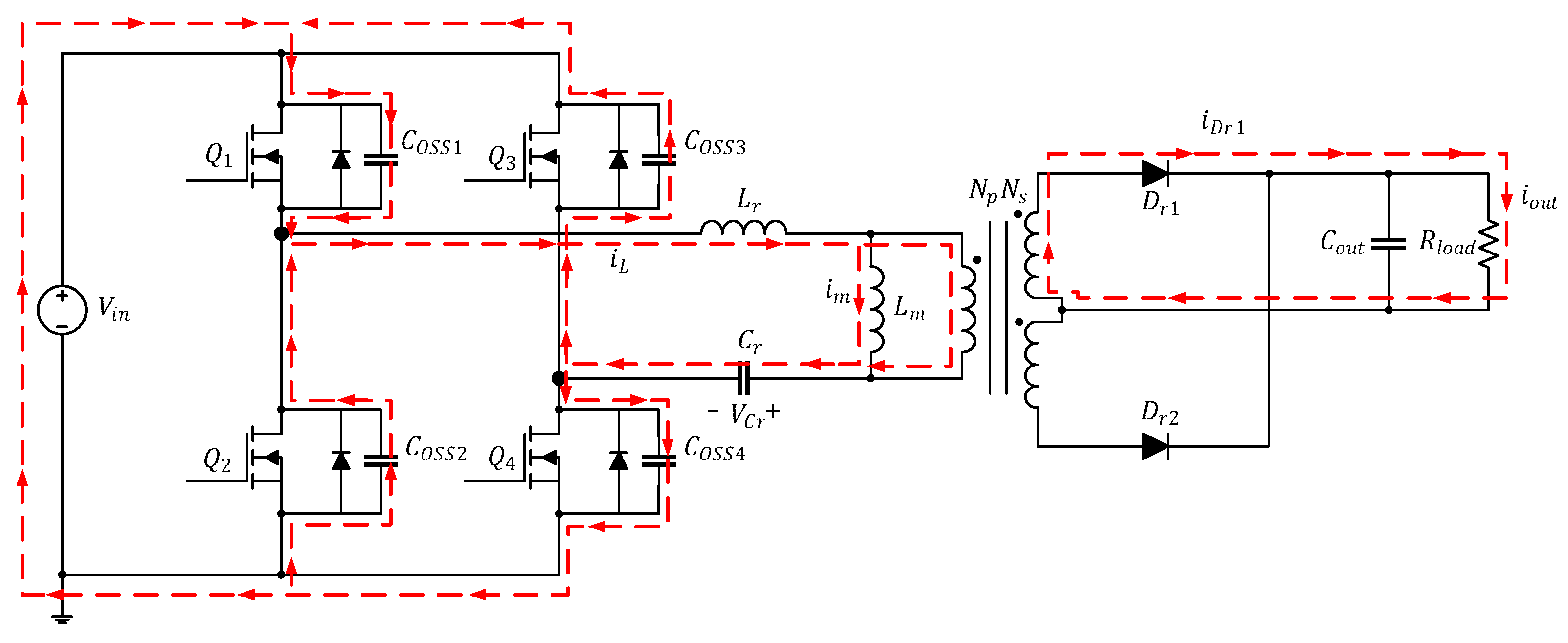
Figure 1 illustrates the circuitry of the full-bridge LLC resonant converter featured in this study. The parameters labeled in the diagram are presented in
Table 2. If the transformer in the converter were ideal, the primary side and secondary side would each form independent loops. The primary side is controlled by using the half-bridge LLC resonant control chip to drive the first-arm power transistors (
and
), then reversing the first-arm signal through the coupling transformer to drive the second-arm power transistors (
and
). The secondary side comprises a full-wave rectification circuit, which is equivalent to a diode (
and
) in circuit analysis.
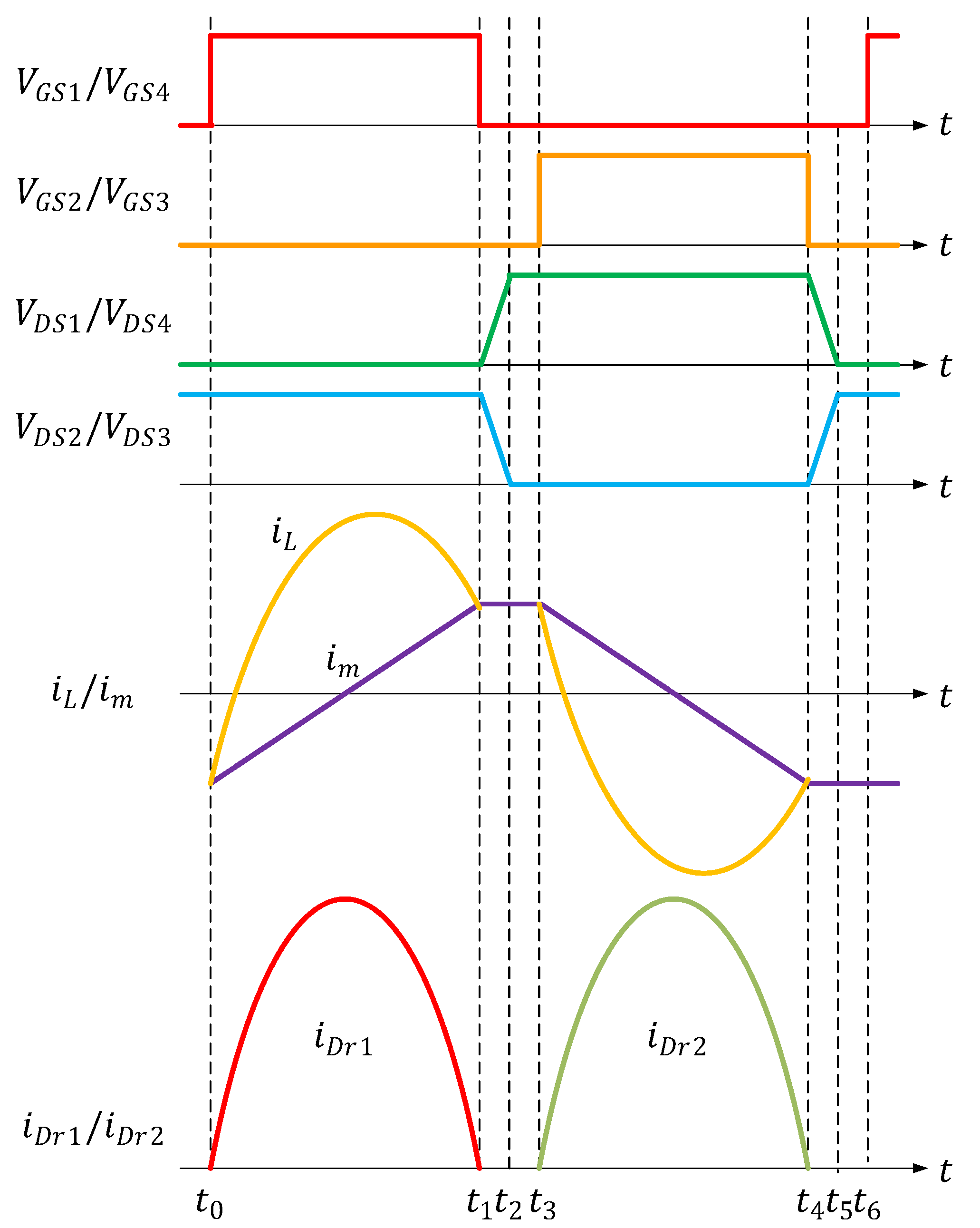
LLC resonant converters typically operate either in the inductive region or the resistive region, which are differentiated by the current mode of the converter.
Figure 2 is a waveform diagram of the LLC resonant converter operating in the resistive region [
14].
In
Figure 2, the circuitry of the full-bridge LLC resonant converter has six modes, designated
to
; the circuit operations are as follows [
15,
16,
17]:
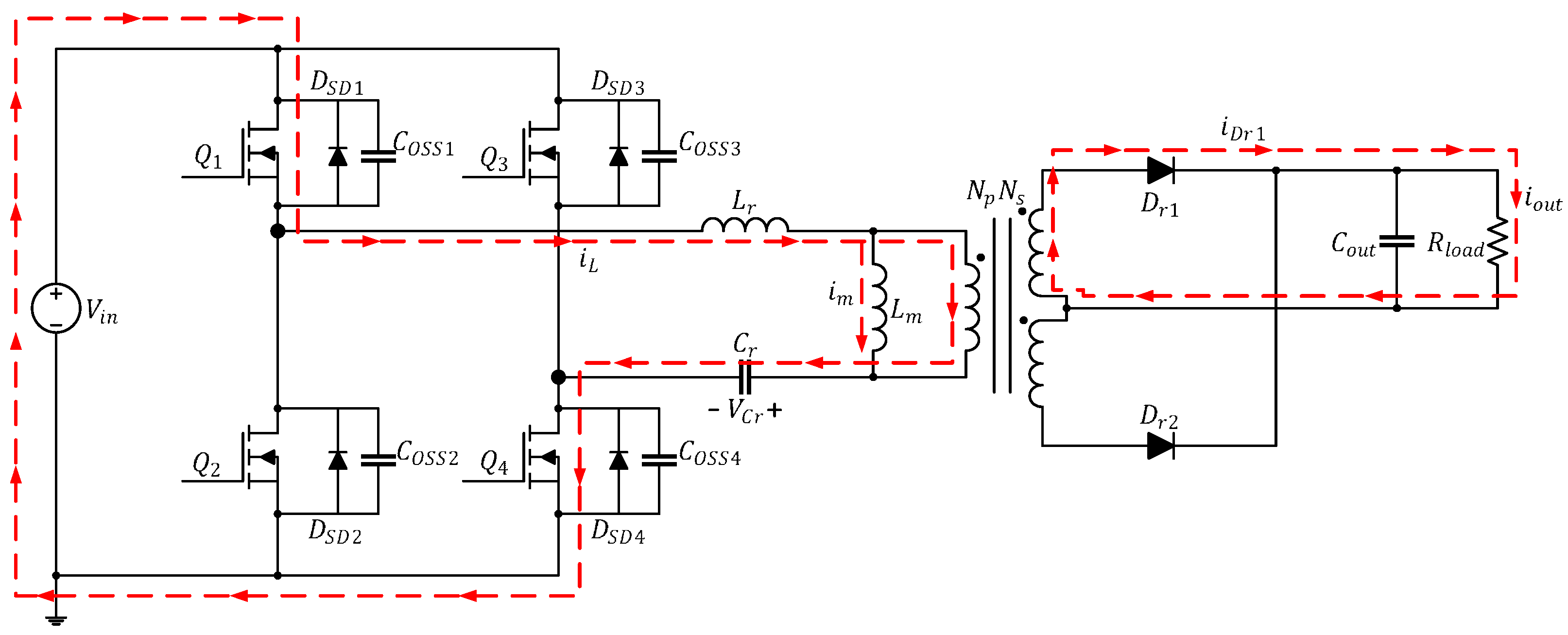
The current path in this mode is depicted in
Figure 3. At time
,
and
are turned on while
and
are cut off; in addition,
flows through
and
and increases positively in a sinusoidal manner while
increases linearly. At this time, because
, the primary side of the converter has a positive half-cycle voltage, and the energy is transmitted to the secondary side through the transformer.
is turned on and generates
to provide energy to
and
. In this mode,
is clamped by the output voltage to
and is not involved in the resonance; only
and
are involved.
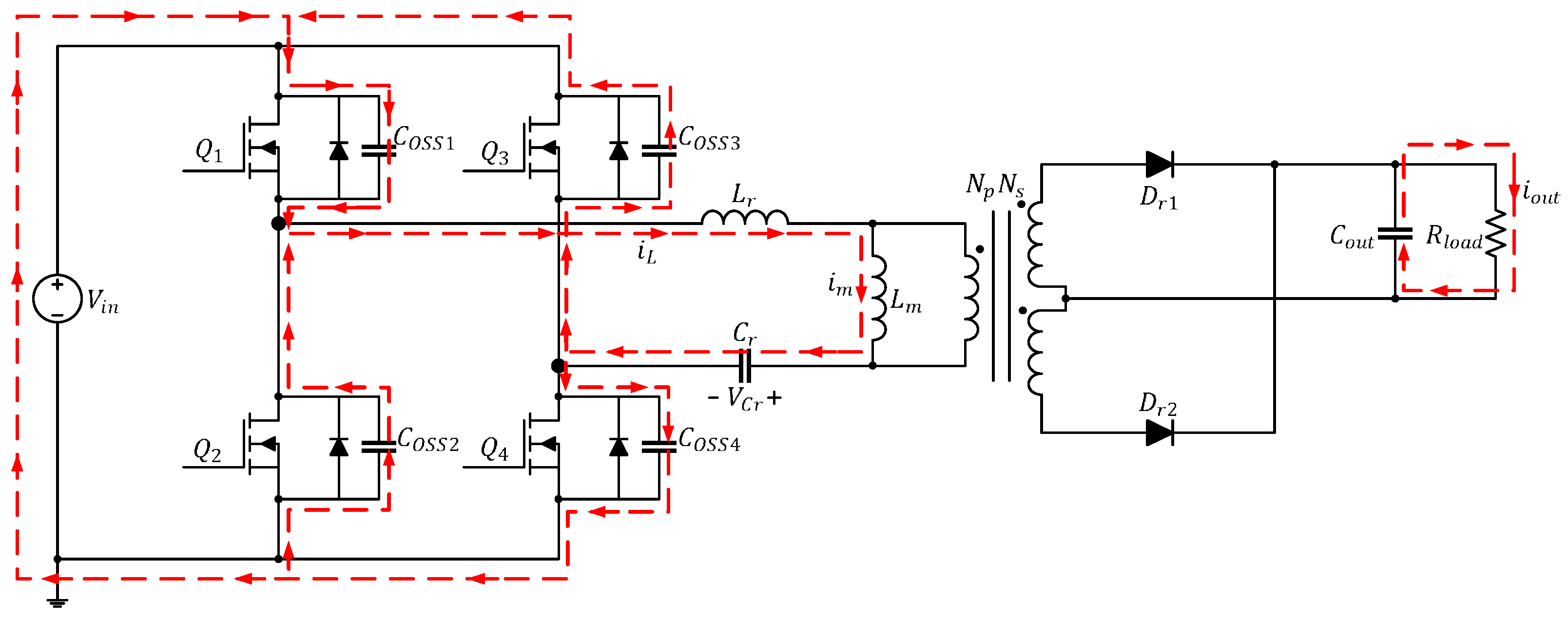
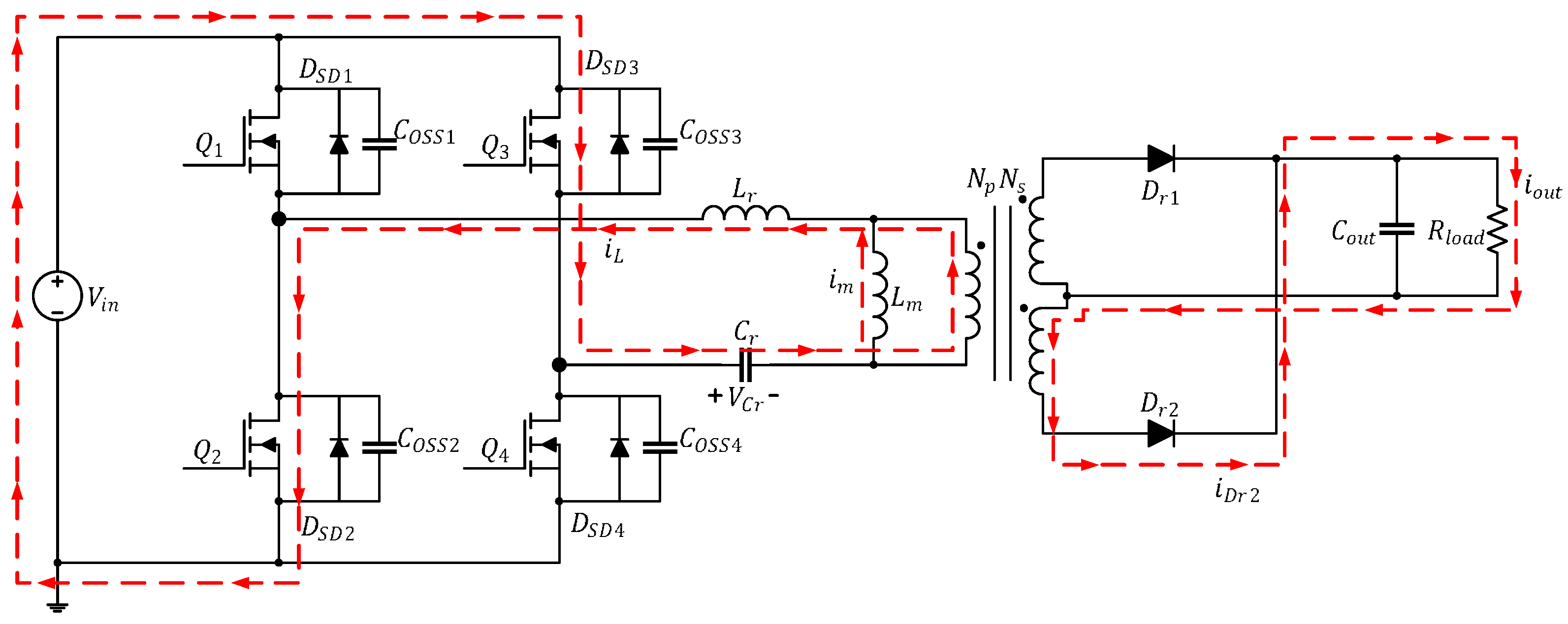
The current path in this mode is depicted in
Figure 4. During this interval, all four power transistors are cut off; because the inductor current cannot be cut off immediately,
and
remain equal, and their directions do not change. The converter makes use of this time interval to transfer energy from the output parasitic capacitor, charging
and
and discharging
and
. During this time, the transformer is not transferring energy, and, consequently,
on the secondary side drops to zero;
is supplied power by
.
is no longer clamped by the output voltage and becomes part of the resonance alongside
and
; at this time,
can be regarded as a fixed current coming from the source.
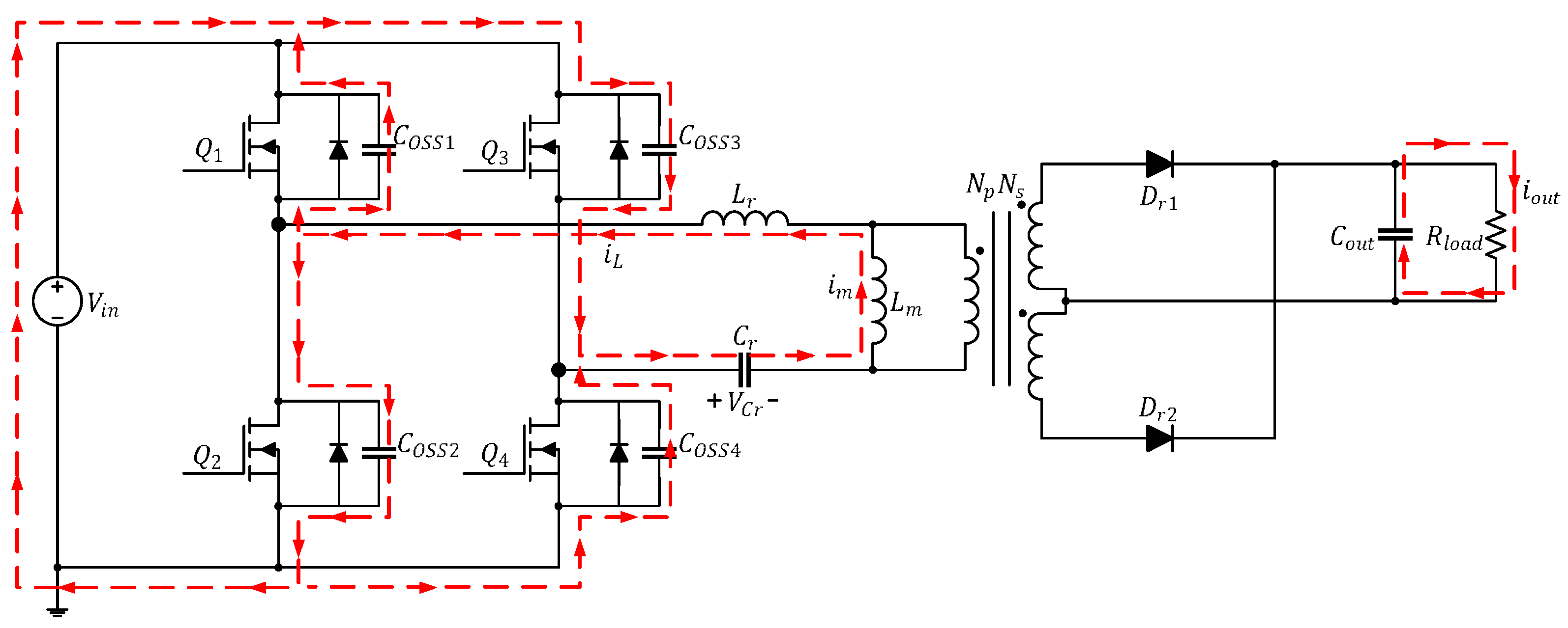
The current path in this mode is depicted in
Figure 5. During this interval, the four power transistors remain cut off. Again, because the inductor current cannot be cut off immediately,
and
remain equal, and their directions do not change. Furthermore, the charging and discharging output parasitic capacitors on the power transistor have been completed, and the remaining energy now flows through the body diode rather than the output parasitic capacitors as before; consequently, the current from the converter flows through
and
during this interval, and the transformer continues to have no energy to transfer.
is still supplied power by
.
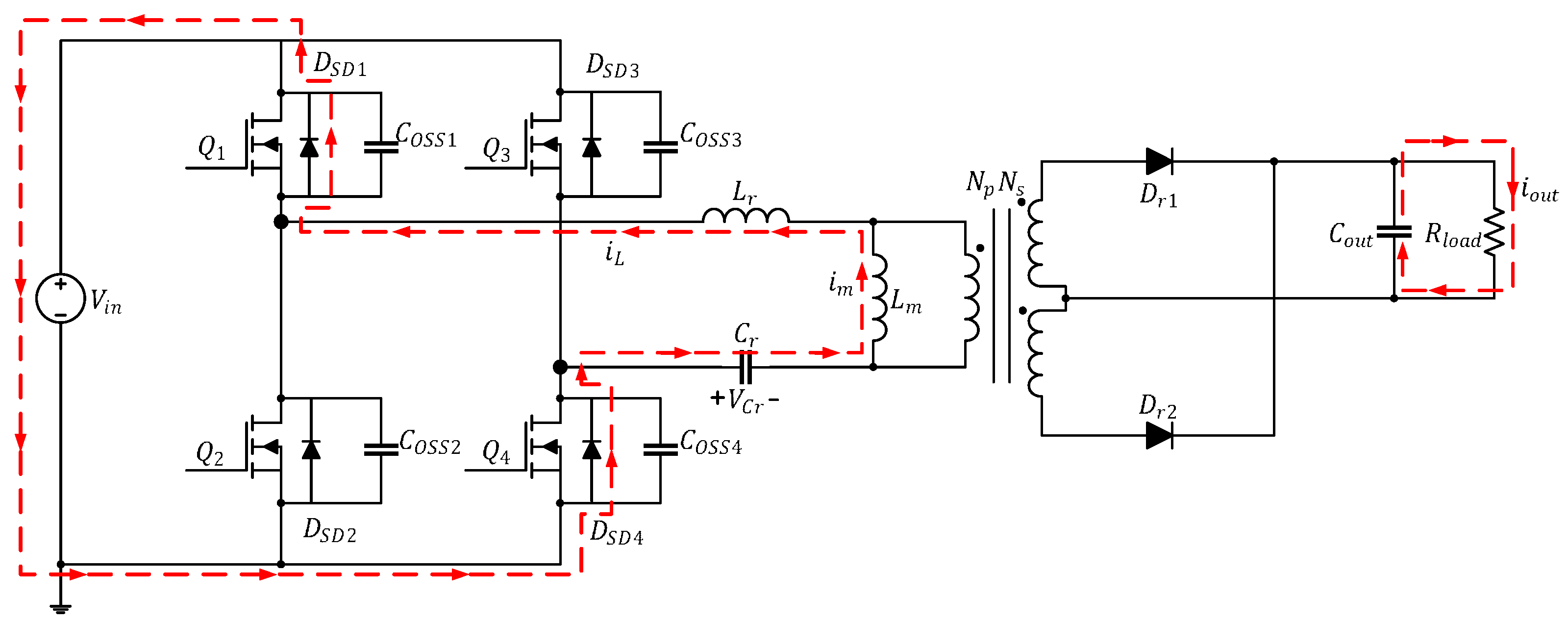
The current path in this mode is depicted in
Figure 6. At time
,
and
are turned on, and
and
are cut off;
passes through
and
and increases negatively in a sinusoidal manner, whereas
decreases linearly. At this time, because
, the primary side of the converter has a negative half-cycle voltage, and the energy is transmitted to the secondary side through the transformer.
is turned on and generates
to provide energy to
and
. In this mode,
is clamped by the output voltage to
and is not involved in the resonance; only
and
are involved.
The current path in this mode is depicted in
Figure 7. During this interval, the four power transistors are cut off; because the inductor current cannot be cut off immediately,
and
remain equal, and their directions do not change. Furthermore, the output parasitic capacitors of
and
are charged, and the output parasitic capacitors of
and
are discharged. During this time, the transformer is not transferring energy; consequently,
on the secondary side drops to zero, and
is supplied power by
.
is no longer clamped by the output voltage and becomes part of the resonance alongside
and
; at this time,
can be regarded as fixed current from the source.
The current path in this mode is depicted in
Figure 8. During this interval, the four power transistors remain cut off. Again, because the inductor current cannot be cut off immediately,
and
remain equal, and their directions do not change. Furthermore, the charging and discharging output parasitic capacitors on the power transistor have been completed, and the remaining energy now flows through the body diode rather than the output parasitic capacitors as before; consequently, the current from the converter flows through
and
during this interval, and the transformer continues to have no energy to transfer.
is still supplied power by
. At this point, the switching cycle is completed and starts again.
3. Effect of Output Parasitic Capacitor on Converter Efficiency
When the LLC resonant converter is under a full load range, the primary-side power transistor operates in the ZVS state. The converter resonates during the dead time to transfer the energy from
of the power transistor (
Figure 6). If the dead time is too short, the
energy cannot be fully transferred, resulting in switching loss. In addition, energy has time to flow through the body diode of the power transistor if the dead time is overly long, increasing the conduction loss of the diode. Hence, the overall efficiency of the converter is affected by the amount of dead time. In practice, the dead time only lasts up until the conversion of
energy is complete. Therefore, the half-bridge LLC resonant control chip employed in this paper adjusts the length of the dead time by detecting whether the
energy has been released. The time needed to release the
energy is determined by the current load, which means that each load has a corresponding
energy release time, which is the corresponding dead time.
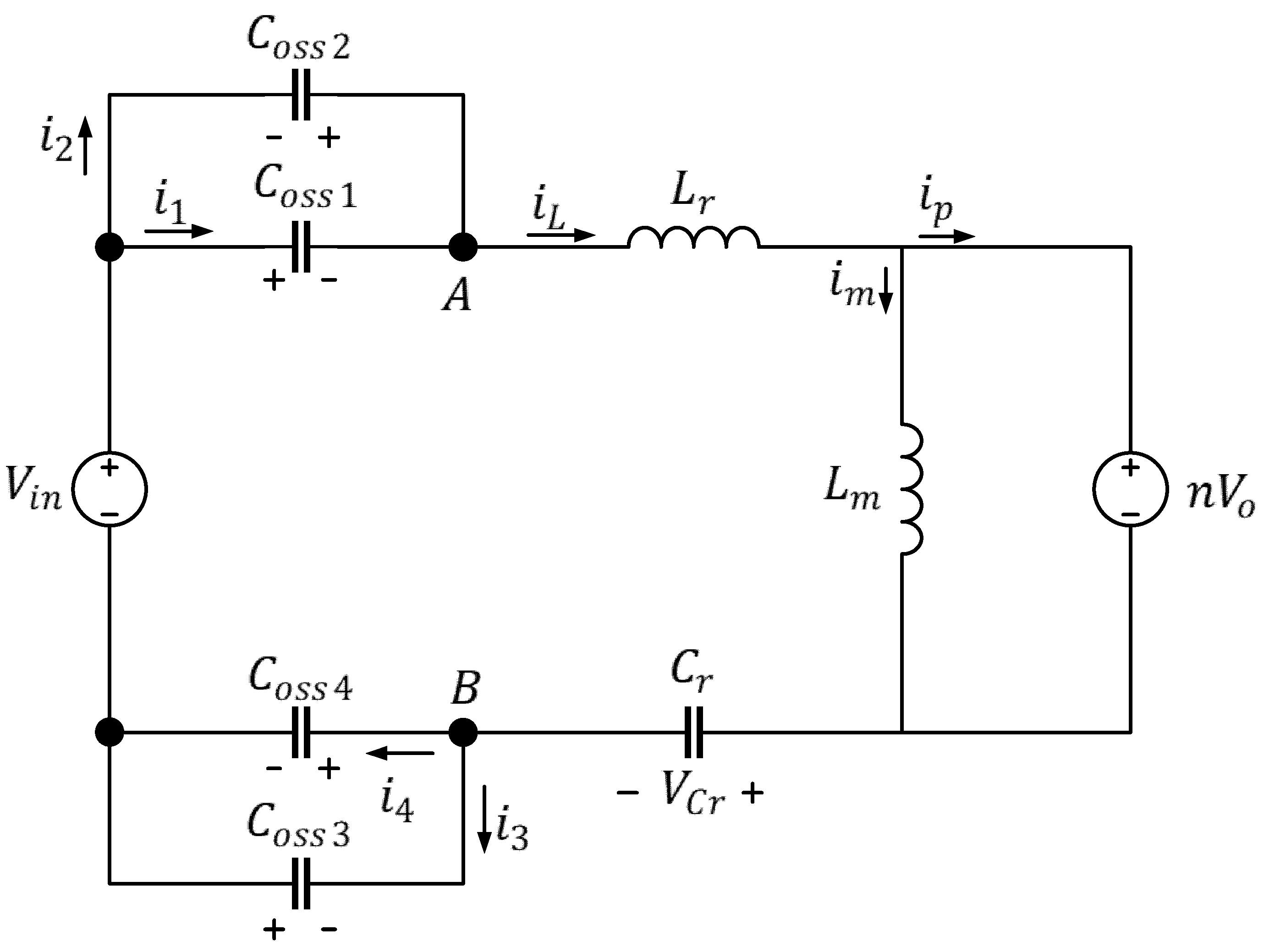
The amount of dead time affects the switching loss and conduction loss of a power transistor. When the system is under a heavy load, the power loss of the converter comes primarily from the iron loss and copper loss of the transformer, resulting in milder effects from switching loss and conduction loss of the power transistor. The effects of dead time under a light load were analyzed in this study. Light loads function in the inductive region, where the operating state is different from that in the resistive region—when the converter is in the resistive region, its current is in critical conduction mode, and, consequently, the transformer has no energy to transfer during the dead time. When the converter is in the inductive region, the current is in a continuous conduction mode, and the transformer continues to transfer energy during the dead time, as depicted in
Figure 9; the equivalent circuit is shown in
Figure 10.
Based on the direction of current, the converter stores energy in
and
and discharges energy from
and
; if the energy transferred in the loop is fixed, the following can be obtained:
Here,
and
are the resonant tank voltage and total charge, and
is a pair of output parasitic capacitors (either
and
or
and
);
is the dead time needed to reach ZVS. If the energy being transferred is fixed, in each state, only one pair of output parasitic capacitors is fully charged. According to
Figure 9, transferring the loop energy to
and
at this time results in the following:
If the input voltage of the resonant tank is
, then, according to
Figure 10,
In Equations (3) and (5), the time needed to reach ZVS in ideal conditions is as follows:
A greater value corresponds to a heavier load and a shorter time required to reach ZVS. Therefore, when = 0 A, the longest ZVS time of the converter is . In this study, the efficiency of the converter under light loads was adjusted, and when the load was 300 W, ideally, .
The primary-side power transistors of the LLC resonant converter can enter the ZVS state under any load. The first-arm power transistors are driven by a half-bridge LLC resonant controller chip, and the second-arm power transistors are driven by the coupling transformer loop; as such, the controller chip is unable to detect the state of the second-arm power transistors. Furthermore, the coupling transformer loop causes signal delays, leading to errors in the driving times of the first-arm and second-arm power transistors; consequently, the second arm is unable to enter the ZVS state.
All four power transistors can enter the ZVS state by adjusting the first-arm
and extending the converter dead time. If any pair of output parasitic capacitors have the same amount of energy, then
Here,
and
are the voltages of the
and
output parasitic capacitors, respectively, and
and
are the dead times needed by the first and second arms, respectively. According to Kirchhoff’s circuit laws, the sum of the potential differences across all components in the loop is zero. Therefore, in the loop,
, yielding
Due to the time differences between the first-arm and second-arm transistors, the second-arm power transistors were unable to discharge all of their energy during the dead time, indicating a need for more time. Hence,
, and by entering
into Equation (6), we obtain:
where
is the adjusted output parasitic capacitance of the first-arm power transistors.
Using Equation (13), we find the appropriate first-arm is , and, using Equation (14), we determine that the first-arm power transistors must be connected in parallel with an output capacitor of .
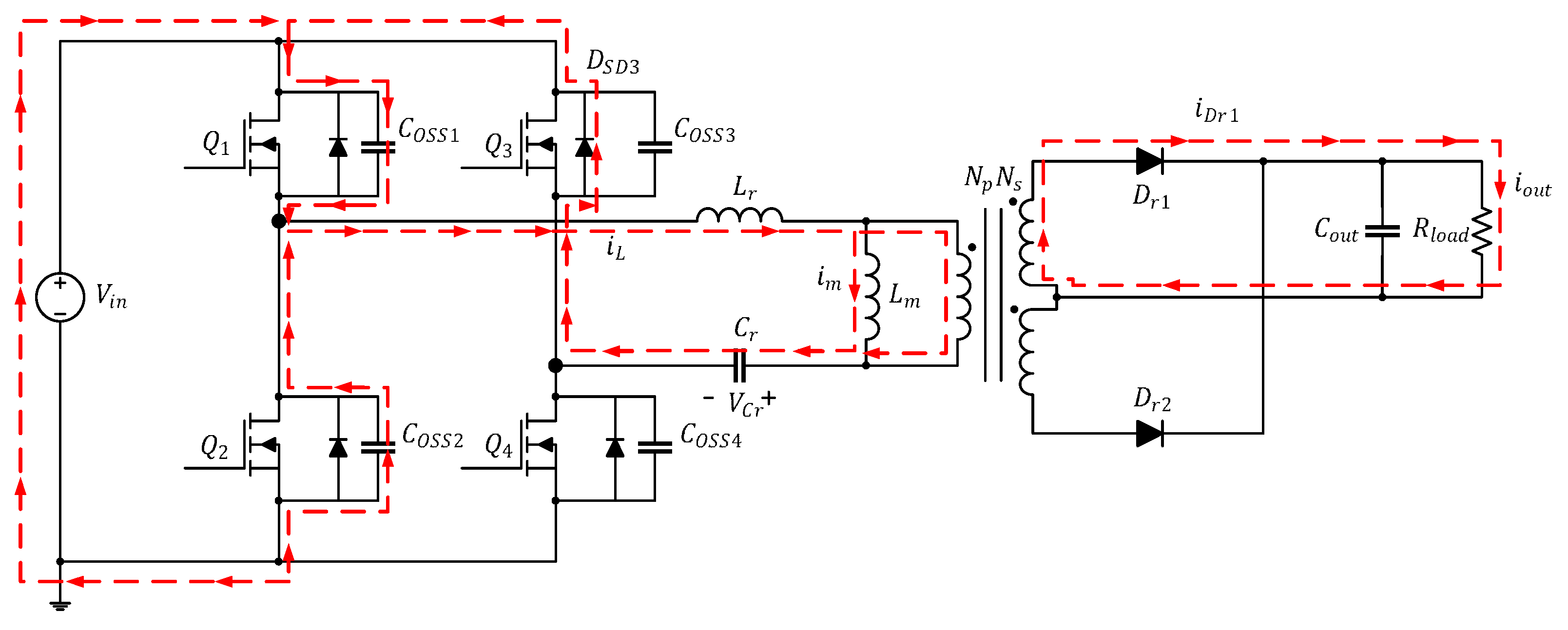
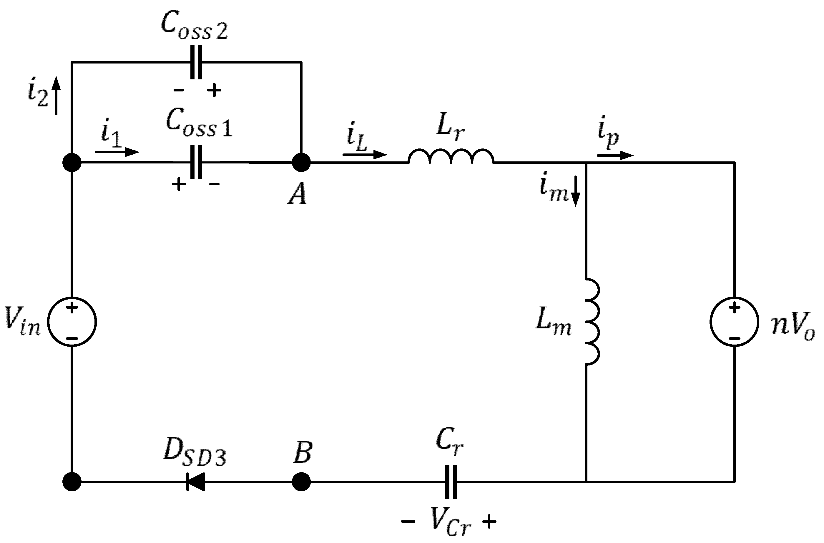
After the four primary-side power transistors have entered the ZVS state, if the first-arm
continues to be increased to extend the converter dead time, because the first-arm power transistors are monitored by the controller chip, the first arm remains in the ZVS state; however, the second-arm power transistors are not monitored, and, therefore, after the energy transfer is complete, the remaining energy of the second-arm
flows through the body diode of the power transistors, as illustrated in
Figure 11; see
Figure 12 for the equivalent circuit.
As illustrated in
Figure 12, an excessive
results in overly long dead times; the conduction loss increased by the second-arm power transistors is
where
: excessive time in the ZVS state
: optimal time in the ZVS state
Equation (14) indicates that when the dead time exceeds , for each additional , the conduction loss by the body diode increases by .
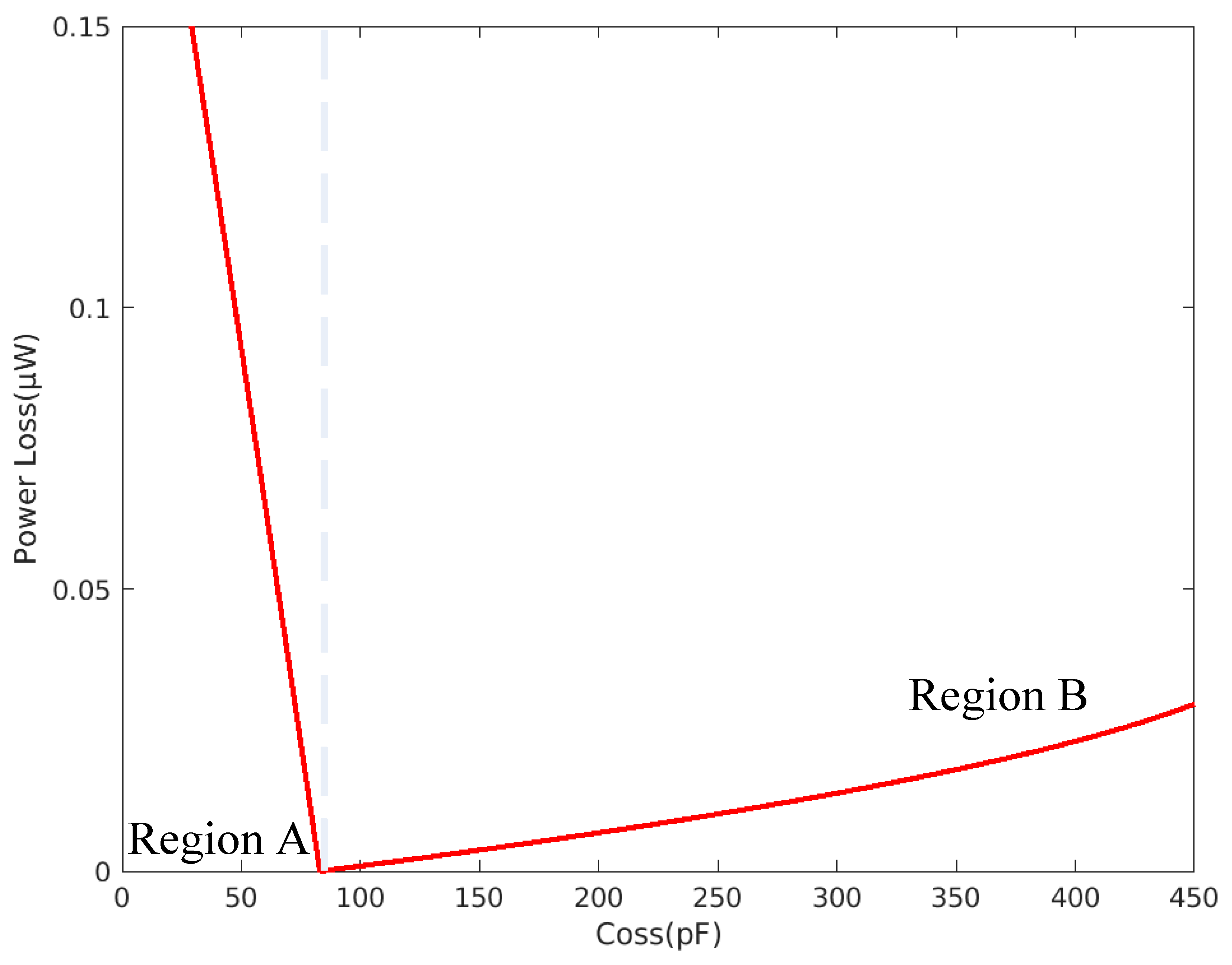
The relationships between
and the switching loss and conduction loss of the primary-side power transistors of the full-bridge LLC resonant converter can be derived from the aforementioned equations (
Figure 13).
The left (Region A) and right (Region B) partitions of the curve in
Figure 13 correspond to values lower and higher than the suitable
value, respectively. Region A is the switching loss caused by the inability of the second-arm power transistors to fully transfer the
energy during the dead time, which is too short because
is too low. Region B is the conduction loss caused by the induction current continuing to flow though the body diode after the second-arm power transistors have finished transferring
because the dead time is too long. The figure demonstrates that loss increases when
is too high or too low. Furthermore, the loss in Region A is greater than the loss in Region B, and therefore, switching loss must be minimized in the design.
4. Experimental Results
The circuitry of the full-bridge LLC resonant converter combined with secondary-side synchronous rectification is depicted in
Figure 14; the component specifications are presented in
Table 3.
The converter’s poor efficiency under light loads was improved by adjusting the
of the power transistors. According to the calculation results of Equation (8), the first-arm power transistors on the primary side must be connected in parallel to a
capacitor to achieve the appropriate dead time; because the
cross voltage of each power transistor is
, a capacitor with a capacitance of
was selected in this study. As indicated in
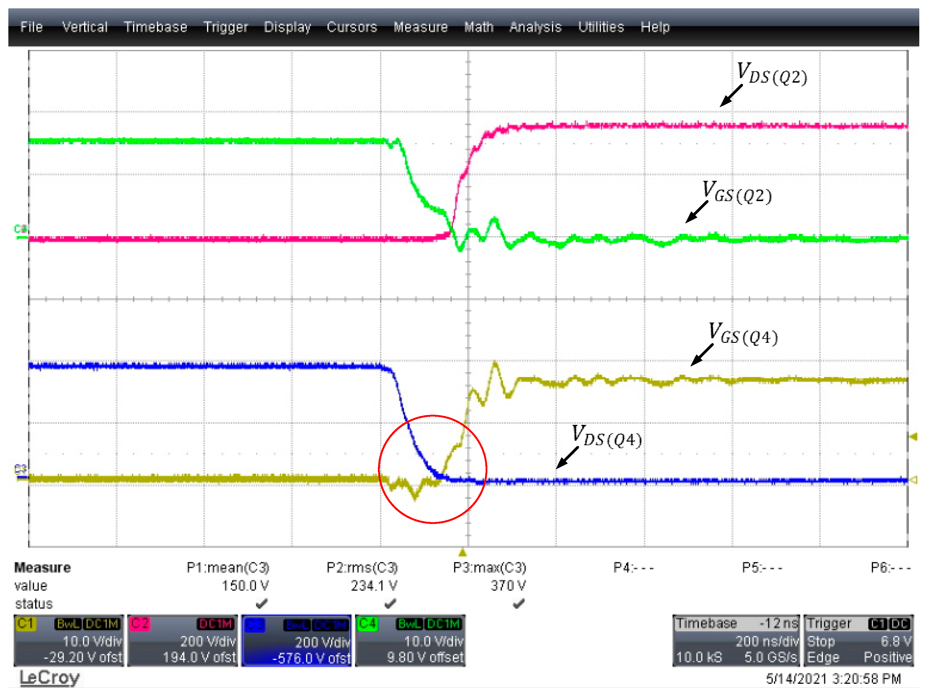
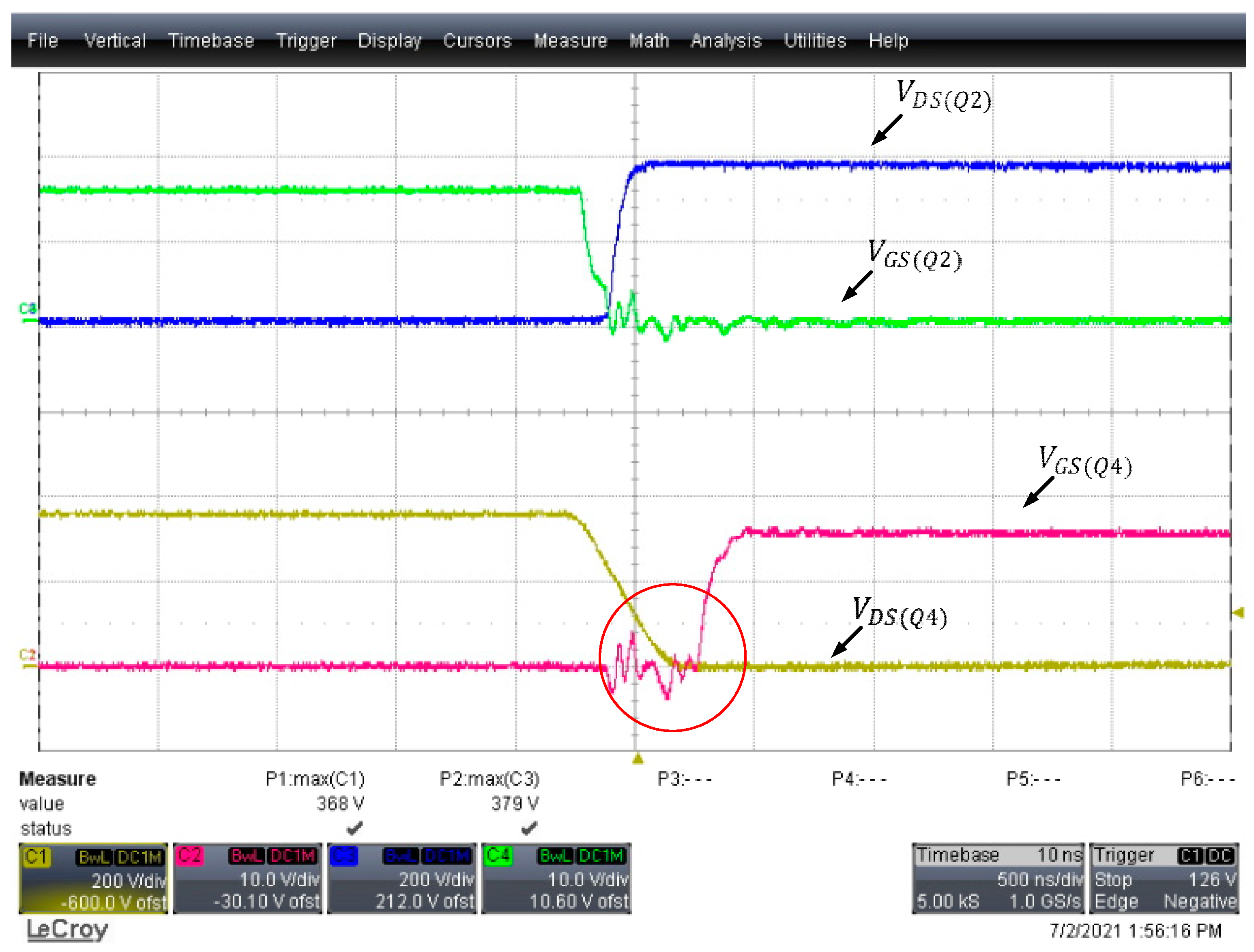
Figure 15, overlap between the power transistors was greatly reduced, indicating noticeable ZVS states, and the measured temperatures of the two low-side power transistors was also greatly reduced. Prior to the adjustments, the second arm was 10 °C warmer than the first arm; after the adjustments, the temperature difference dropped to 0.5 °C.
According to the results of Equation (15), if the first-arm
is continually increased, the first arm remains in the ZVS state, while in the second arm, the remaining energy flowing through the body diode of the power transistors during the unnecessary dead time leads to conduction loss. As shown in
Figure 16, after the transfer of the parasitic output capacitor energy, the power transistors failed to immediately change states.
.
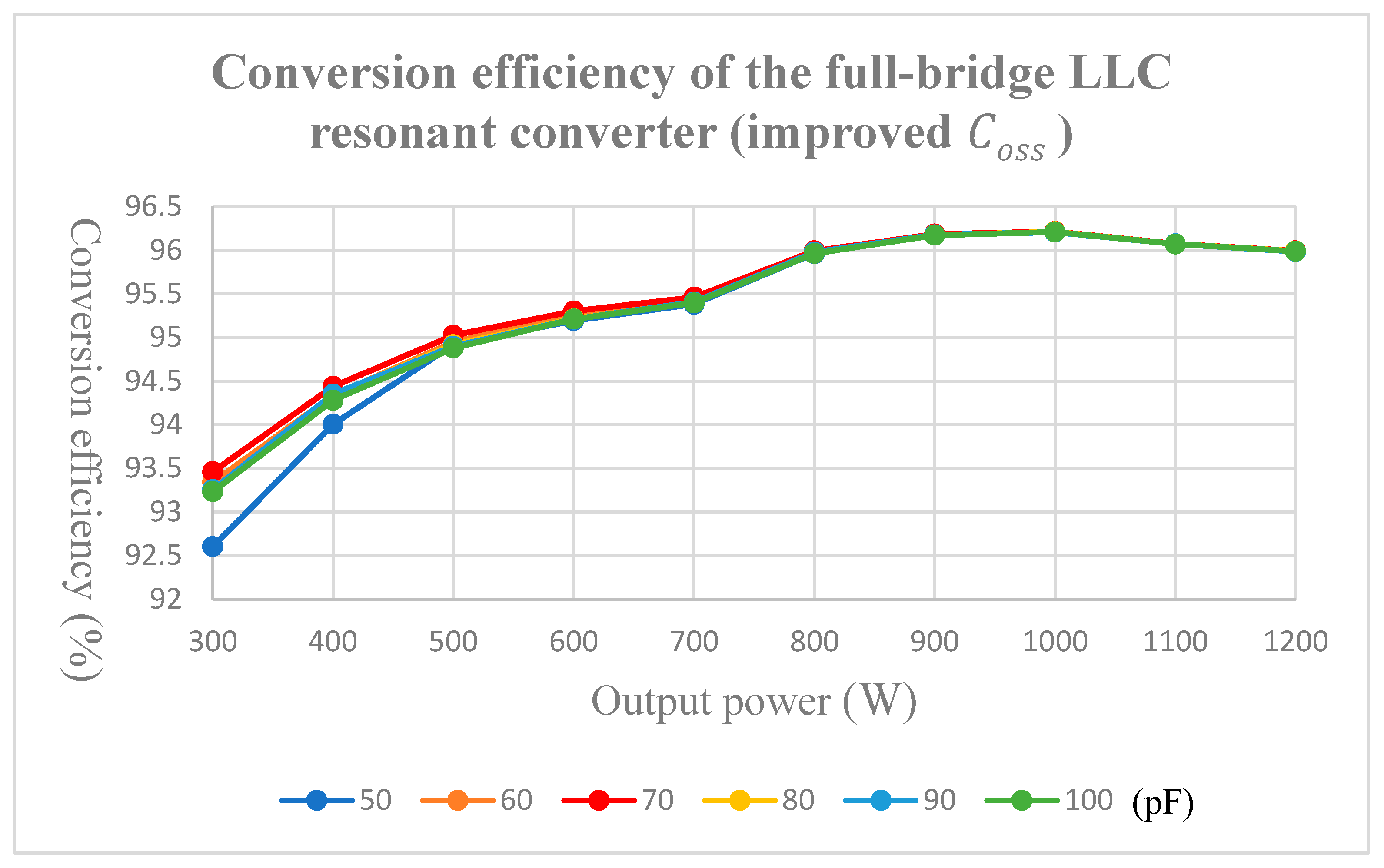
When the converter is under a heavy load, the copper loss and iron loss of the transformer is greater than the switching loss and conduction loss of the power transistors. Furthermore, adjusting the
value does not significantly improve the efficiency. Hence, the
experiment in this paper was conducted under a light load, where components with
and
were connected parallel to each other; the observed efficiency changes are depicted in
Figure 17. According to the empirical results, when the first-arm power transistors were connected in parallel to the component with
=
, relative to a parallel connection with an unadjusted parasitic capacitance of
, the efficiency for 300 and 600 W were higher
for 300 W) and
vs.
for 600 W).


