Article

A Buried Thermal Rail (BTR) Technology to Improve Electrothermal Characteristics of Complementary Field-Effect Transistor (CFET)

1
School of Microelectronics, Fudan University, Shanghai 200433, China
2
Shanghai Integrated Circuit Manufacturing Innovation Center Co., Ltd., Shanghai 201203, China
*
Authors to whom correspondence should be addressed.
Micromachines 2023, 14(9), 1751; https://doi.org/10.3390/mi14091751
Submission received: 29 July 2023 / Revised: 3 September 2023 / Accepted: 4 September 2023 / Published: 7 September 2023
(This article belongs to the Special Issue Recent Advances in CMOS Devices)

Abstract

:
The complementary field-effect transistor (CFET) with N-type FET (NFET) stacked on P-type FET (PFET) is a promising device structure based on gate-all-around FET (GAAFET). Because of the high-density stacked structure, the self-heating effect (SHE) becomes more and more severe. Buried thermal rail (BTR) technology on top of the buried power rail (BPR) process is proposed to improve heat dissipation. Through a systematical 3D Technology Computer Aided Design (TCAD) simulation, compared to traditional CFET and CFET with BPR only, the thermal resistance ( R t h ) of CFET can be significantly reduced with BTR technology, while the drive capability is also improved. Furthermore, based on the proposed BTR technology, different power delivery structures of top-VDD–top-VSS (TDTS), bottom-VDD–bottom-VSS (BDBS), and bottom-VDD–top-VSS (BDTS) were investigated in terms of electrothermal and parasitic characteristics. The R t h of the BTR-BDTS structure is decreased by 5% for NFET and 9% for PFET, and the I o n is increased by 2% for NFET and 7% for PFET.

1. Introduction

Due to the insurmountable technical challenges of the silicon-based physical layer, as well as the current social development of the era, the demand for computing performance of consumer electronic products tends towards saturation. The semiconductor miniaturization process will be gradually slowed down, which has become a general consensus in the industry. The semiconductor miniaturization process marked by the ‘technology node’ has been extended from the original 18-month cycle to a 24-month cycle [1]. At the same time, the industry is constantly targeting small-size devices in the range of a few nanometers to improve the IC performance, such as Fin field-effect transistor (FinFET) [2,3] and Gate-All-Around Nanosheet FET (GAA-NSFET) [4,5]. Nowadays, using basic rules alone is no longer enough to scale standard cells. It is expected that in the near future, NFET and PFET can be stacked on top of each other for further scaling. The complementary FET (CFET) is one of the most promising devices, which stacks N-type FET (NFET) on P-type FET (PFET) vertically to form an inverter. Such studies have been verified by many institutions, such as IMEC [6], Intel [7] and Applied Materials [8]. It is recognized that GAA-NSFET will replace FinFET below N2, and sheet-based CFET has been proven to have a better performance than fin-based CFET [3].
Recently, several studies have shown the importance of parasitic capacitance in CFET [9,10,11]. Compared with NSFET, CFET shows the possibility of a better performance in frequency and power because of the lower effective capacitance ( C e f f ) [9]. In addition, several studies have shown the importance of SHE in multi-gate transistors such as GAA-NSFET. Their tight geometric construction and difficulty in heat conducting will cause device performance degradation and thermal reliability issues [12,13,14]. Recently, some studies have also been carried out on the electrothermal characteristics of CFET. Device design guidelines for a 3 nm node CFET have been investigated from the perspective of electrothermal characteristics [15]. The self-heating effect (SHE) of the CFET has been investigated, and a cross-coupled thermal network model has been proposed [16].
In almost all previous studies, the issue of electrothermal characteristics in CFET has not been studied comprehensively, which should greatly impact the circuit performance. Due to the longer length of the metal via and higher stacking density, it is expected that the heat dissipation will become more severe. Thanks to the backside power delivery network (BPDN) and buried power rail (BPR) technology [17], there are multiple choices and more spaces for depositing the metal via. However, there are no qualitative analyses of the influence of different via strategies on CFET performance.
For the first time, buried thermal rail (BTR) technology is proposed. Different methods of CFET are compared in terms of electrothermal characteristics and parasitic capacitance. A comparison between different PDN methods with a BTR reveals the performance advantage of CFET architecture. Here, the influence of different parameters on the CFET are well studied.

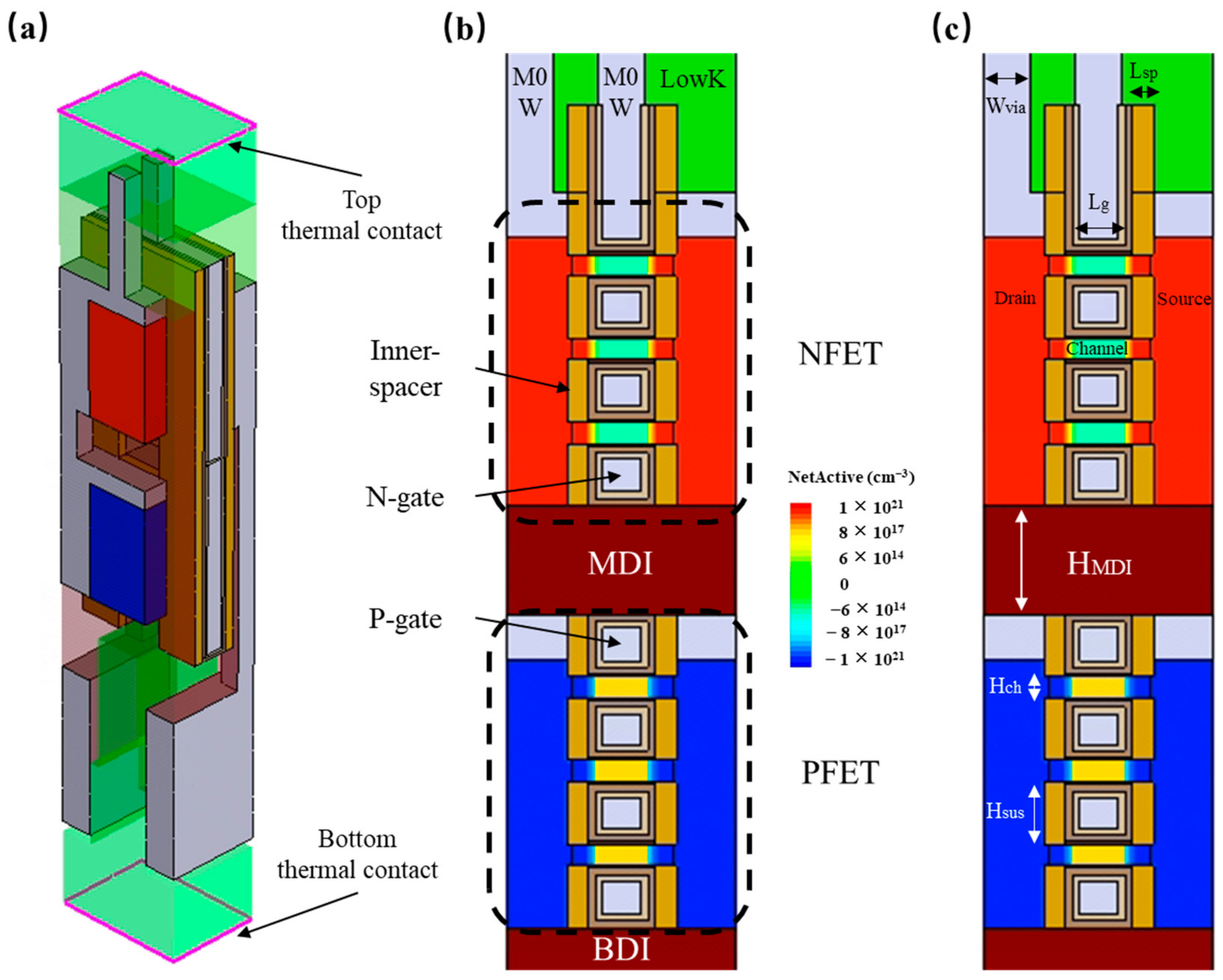
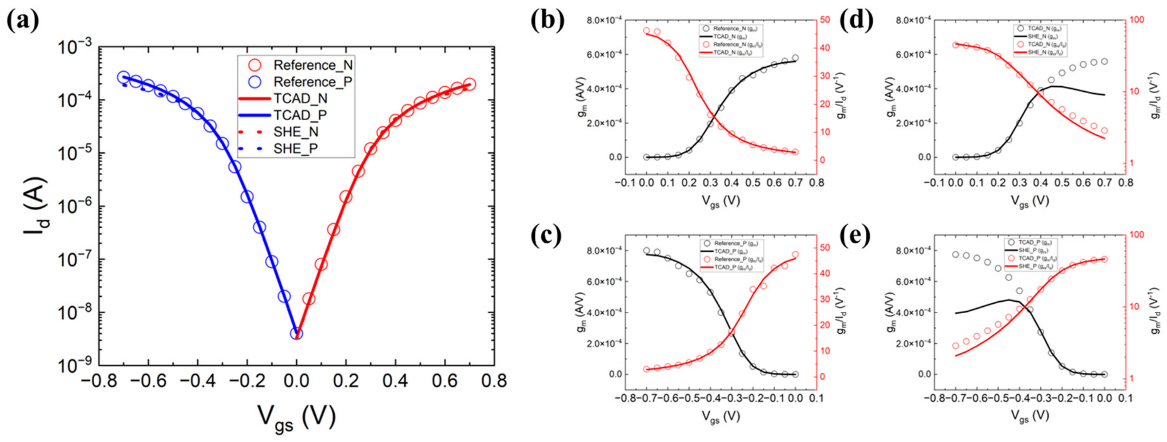
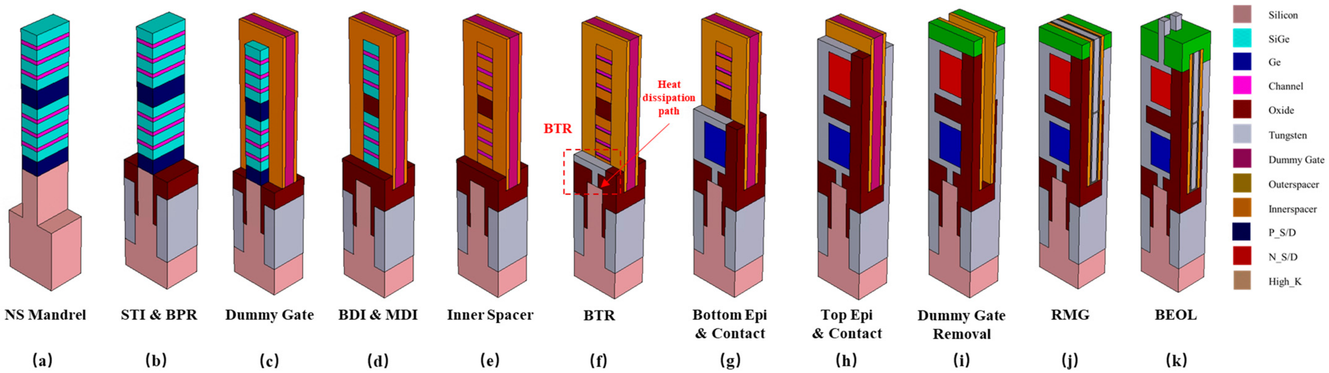
2. Modeling Methodology

The CFET was designed based on the studies released from IMEC [18] and the IRDS2022 [1] in the Sentaurus 3-D Technology Computer Aided Design (TCAD) platform. The electrical and structural parameters of CFET were calibrated with the experimental reference of IMEC [19]. Figure 1a shows the 3D view of the CFET. Figure 1b,c show the cross-sectional view of the CFET and its structural parameters. Table 1 shows the electrical and structural parameters of the CFET. The NFET was stacked on the PFET. The gate length was set as 12 nm, while 0.5-nm-thick gate oxide and 1.5-nm-thick HfO 2 were used. For the gate metal work function, 4.42 eV and 4.84 eV were set to the NFET and PFET, respectively, in order to meet 4 nA/FET off-current. The channel doping concentration of NFET and PFET is 1 × 10 15   cm 3 and 1 × 10 18   cm 3 , respectively, which is consistent with the calibrated structural parameters and remains constant in subsequent simulations. The source/drain doping concentration of both FETs is 1 × 10 21   cm 3 , whose extension doping concentration is 3 × 10 20   cm 3 . An ohmic contact resistivity between the metal and source/drain was also considered, which was set as 1 × 10 9   Ω · cm 2 .
In order to obtain an appropriate heat conduction at the scale of nanodevices, the relevant thermal transmission model in this paper adopts Holland’s model based on the Boltzmann transport equation (BTE), which is calculated using Equation (1) [20]:
κ = 1 3 · j v j 2 0 θ j T C V , j x ω , T τ j x ω , T d x ω
where v j represents the phonon group velocity, θ j represents the Debye temperature, C V , j represents the phonon-specific heat per unit volume, and τ j represents the phonon scattering rate. The subscripts j = T, TU, and L represent transverse and longitudinal modes. x ω = ω / k B T is the nondimensional phonon frequency, k B = 1.38 × 10 23   J · K 1 is the Boltzmann constant, and = 1.055 × 10 34   J · s is Planck’s constant divided by 2 π . Table 2 shows the thermal parameters of the CFET. The top thermal contact resistivity was set as 4 × 10 5   cm 2 · K / W according to its area to achieve a situation close to the actual environment [21]. Benefitting from the BPDN and BPR technology, the bottom thermal contact was set as the same value as its top, as the backside PDN kept the same metal via density, which should not be a difficult objective to achieve. The thermal resistance between the interfacial oxide and silicon channel was also considered, which was set as 2 × 10 4   cm 2 · K / W [22]. The global environment temperature was set as 300 K.
In order to simulate the distribution of the lattice temperature, which is caused by the SHE, both the diffusion drift model and thermodynamic model were included. As the thickness of the channel is 5 nm, the quantum confinement effect and the degradation of mobility in the thin layer should not be ignored. Thus, the density gradient quantization model and the thin-layer model were included. The remote Coulomb scattering model, Philips unified mobility model, and enhanced Lombardi model were used to account for the degradation of mobility, which was caused by degraded carrier mobility, electron–hole scattering, and phonon scattering. In a high electric field, the velocity of carriers is confined, so a high-field saturation model was included. The doping-dependent mobility model, bandgap narrowing model, and Shockley–Read–Hall doping dependence model were also adopted.
The Id-Vg curves shown in Figure 2a, the gm-Vgs and gm/Id-Vgs curves for the NFET and PFET shown in Figure 2b,c and the gm-Vgs and gm/Id-Vgs curves for the NFET and PFET with SHE shown in Figure 2d,e ensure the rationality of the device parameter settings of the CFET in a double-fin structure [19]. Reference_N means the reference data of the NFET. TCAD_N means the TCAD simulation result of the NFET. SHE_N means the TCAD simulation result of the NFET with a self-heating effect, and the same applies for the PFET. The work functions of NFET and PFET were adjusted to match the off-current and the threshold voltage. By default, the velocity in the Drift-Diffusion (DD) simulation cannot exceed the saturation value, which is the reason for the underestimation of the drive current. the DD simulations can be adjusted to match the Monte Carlo (MC) simulation results by increasing the saturation velocity in the mobility model. Increasing the v s a t value of the NFET and the PFET to 3.21 × 10 7   cm / s and 2.51 × 10 7   cm / s , respectively, which are three times the original value, leads to a better fitting of the Id-Vg curves. The Id-Vg curves of double-fin-based CFET with SHE are also shown. When the V g s rises, the I d rises. The increment in the I d increases the temperature, which causes the degradation of the I d , causing the decrement of the g m . The SHE also degrades the device performance, which can be observed by the decrement of the g m / I d . The calibrated model based on the DD is a simplified scheme to avoid the computationally expensive SHE approach. It is used to provide an approximate solution of the carrier transport, which explains the large differences exhibited in Figure 2d,e. Sheet-based CFET has been proven to have a better performance than fin-based CFET; the following research has been established on sheet-based CFET with similar parameters and models. BTR technology has the potential to improve the performance of the CFET. Figure 3 shows the process flow of sheet-based CFET with BTR.

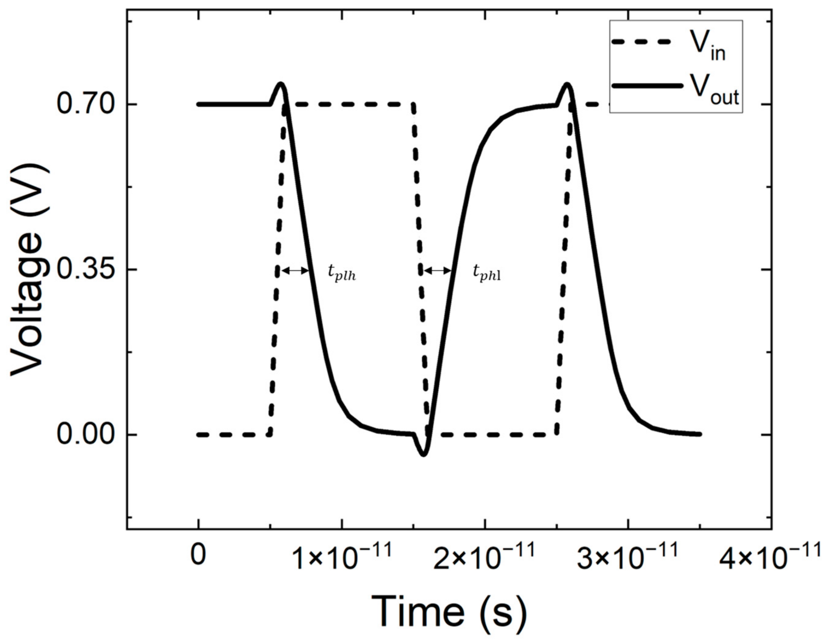
3. Results and Discussion

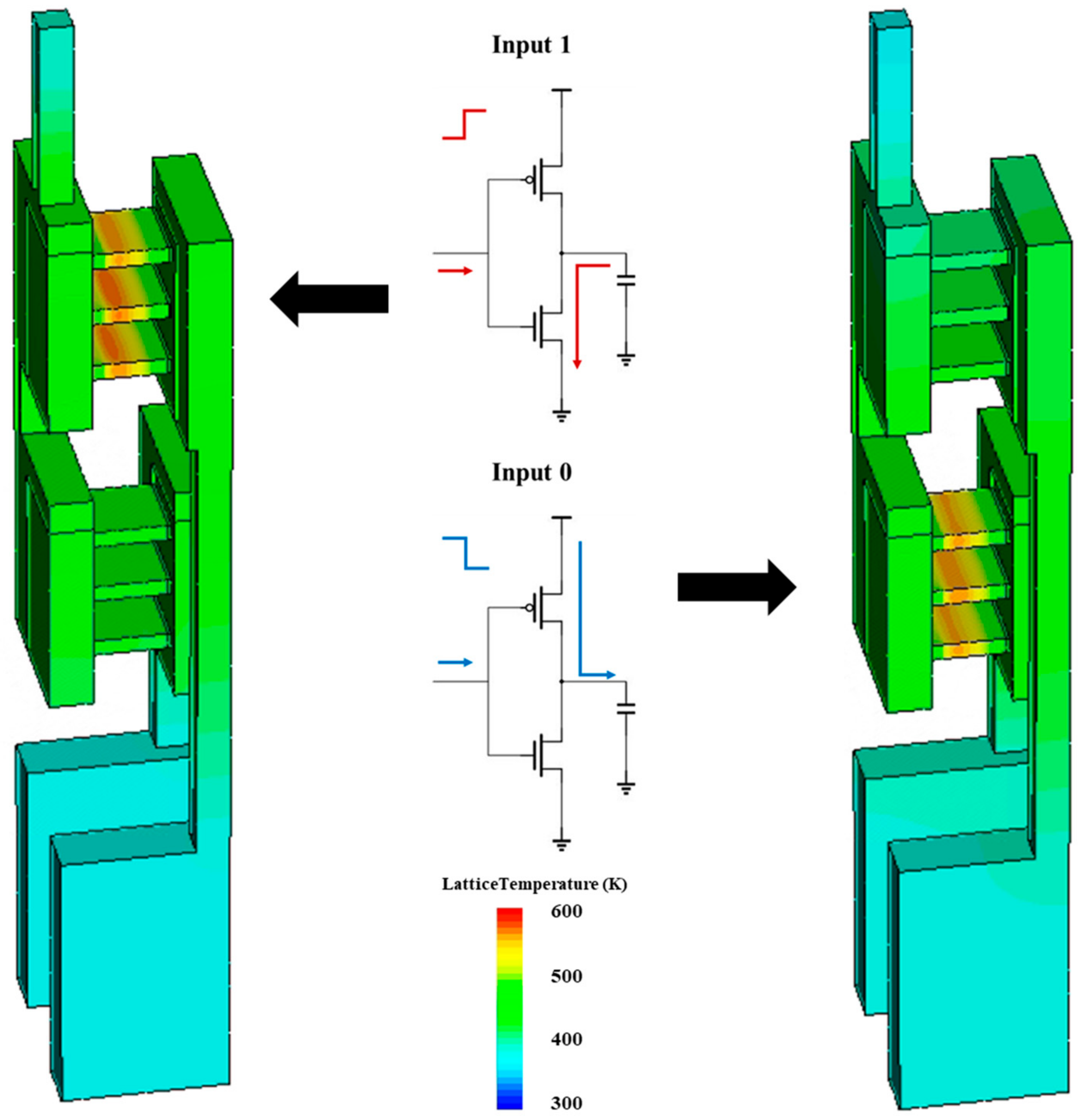
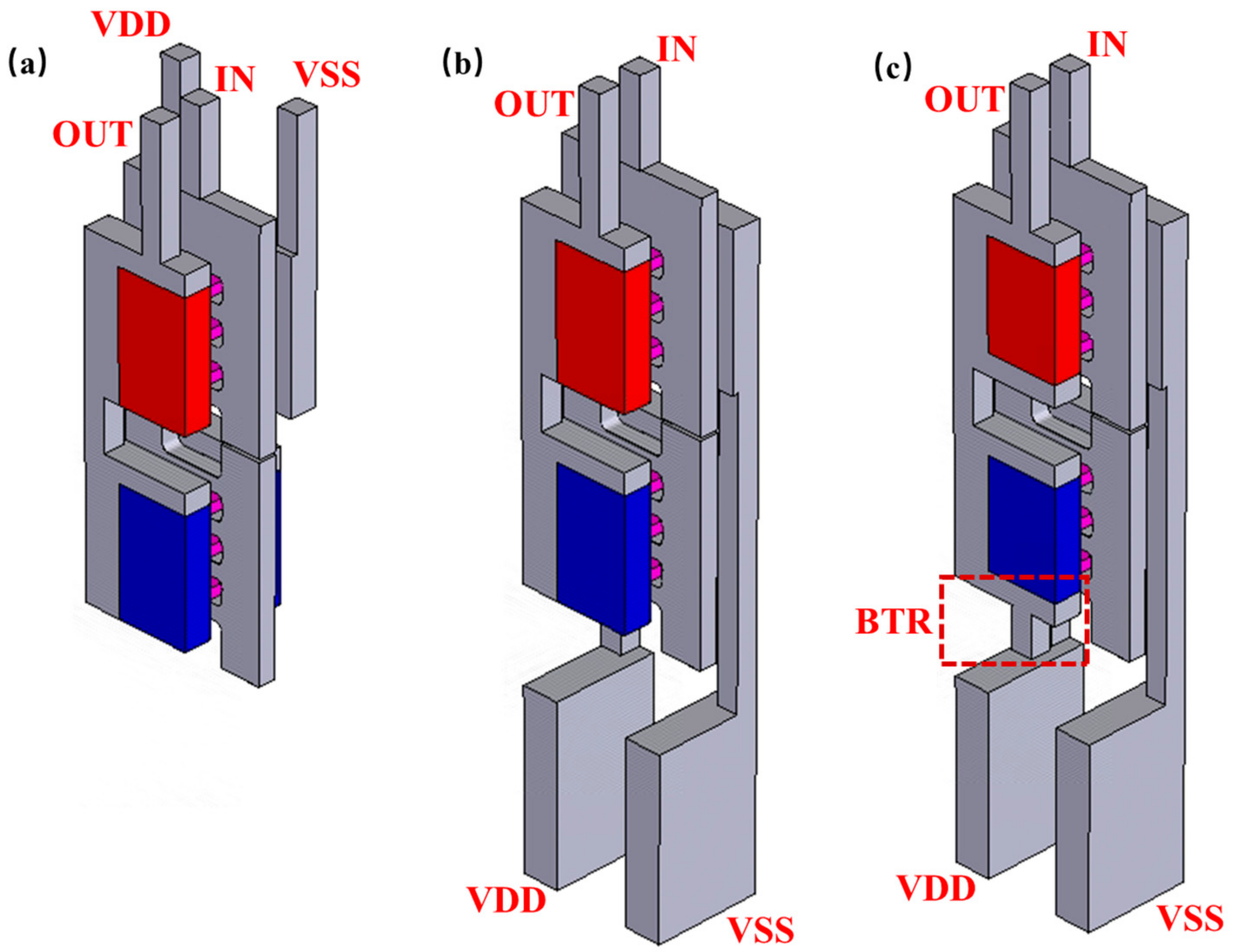
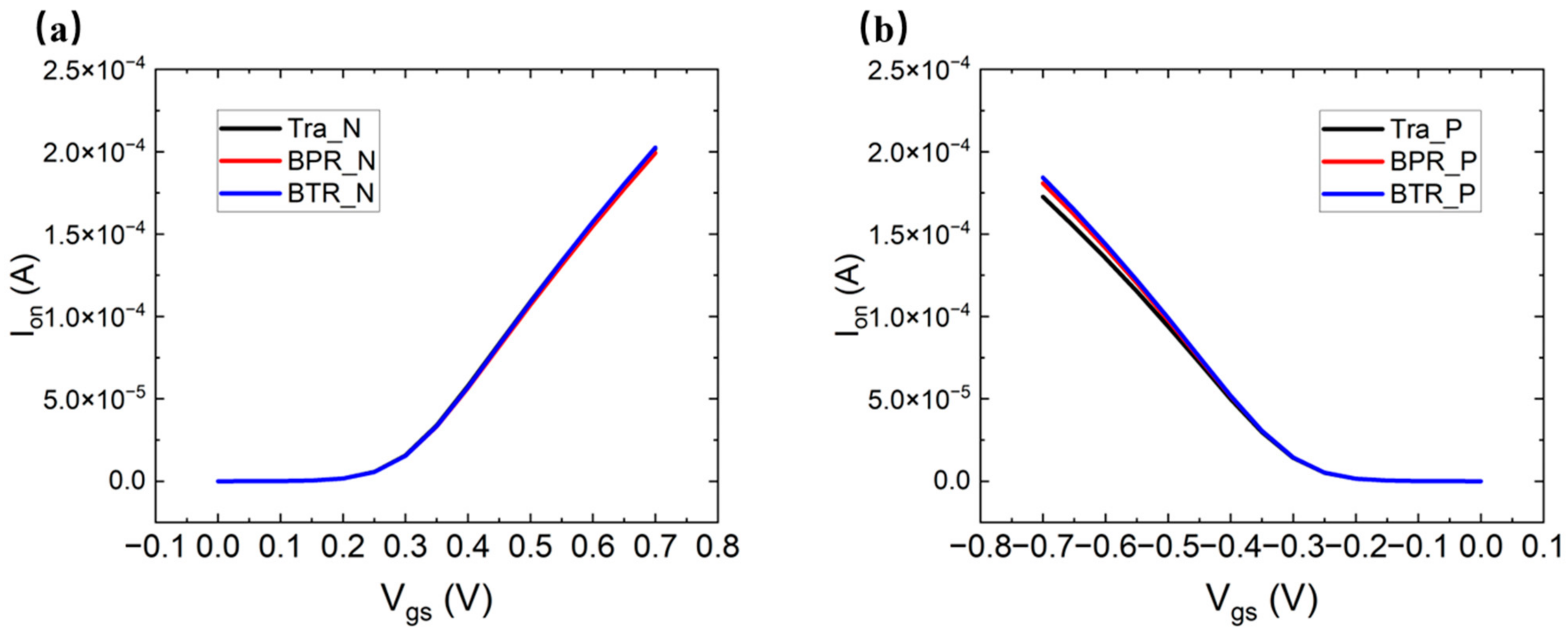
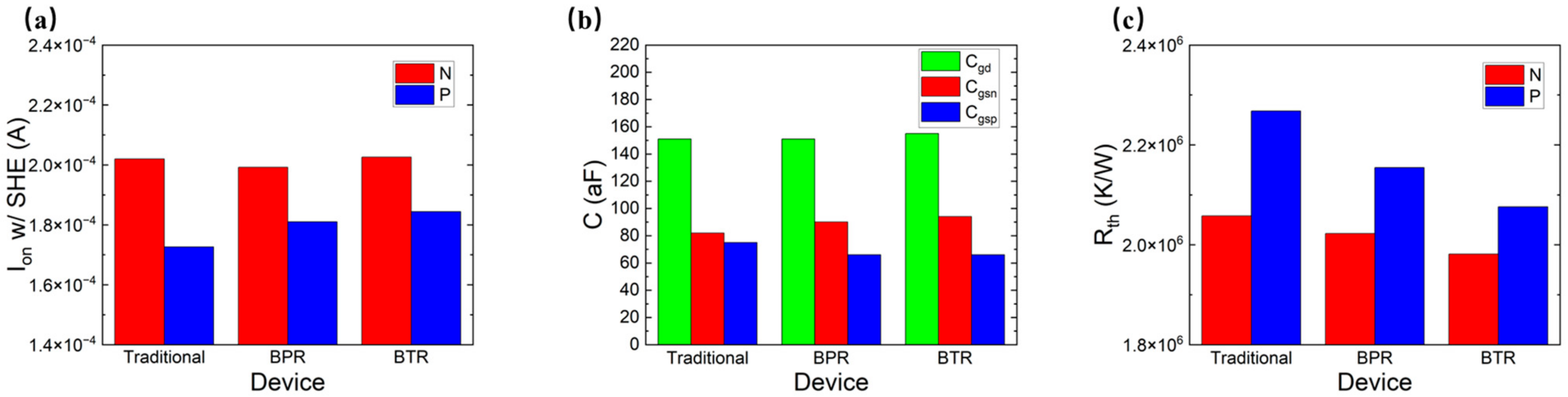
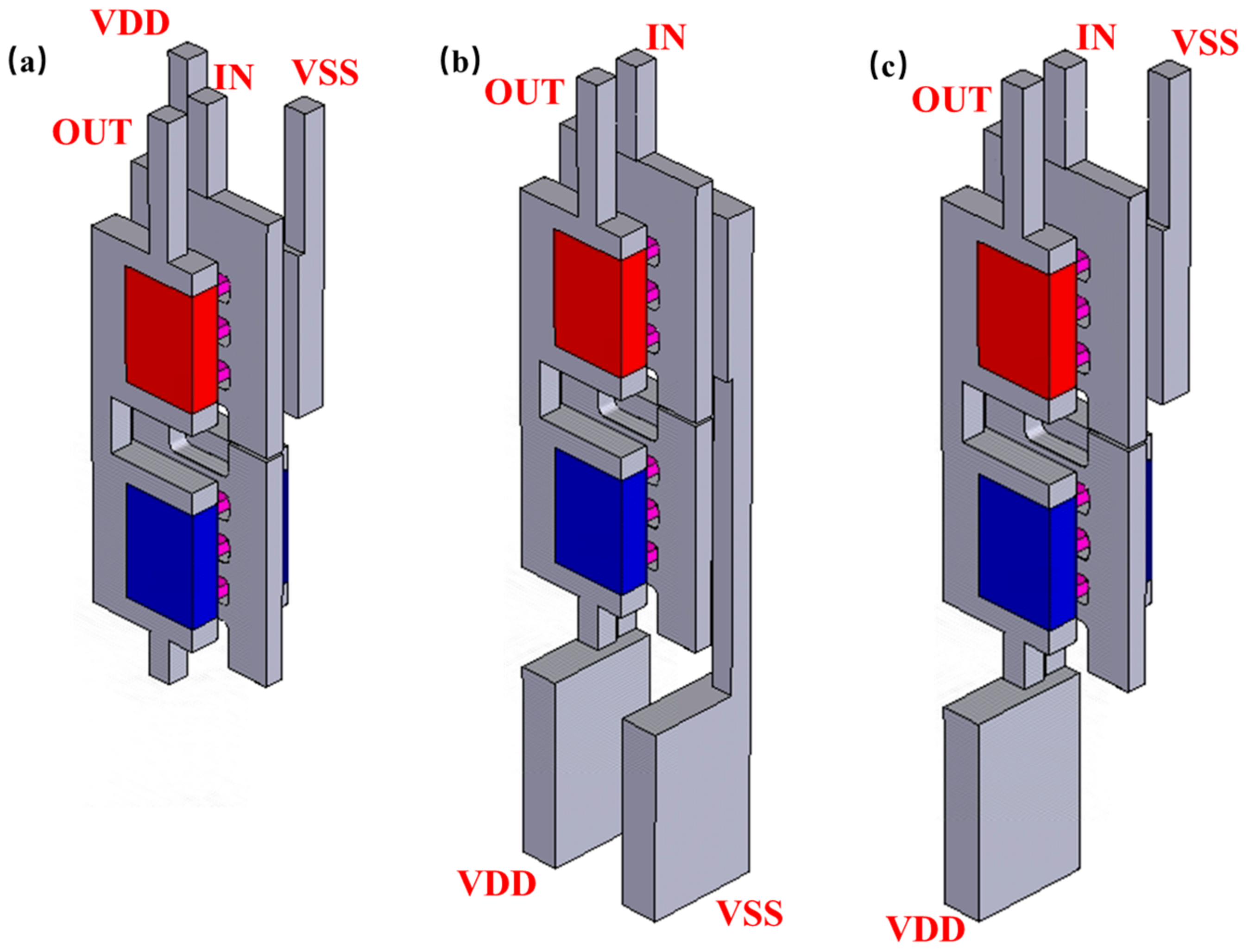
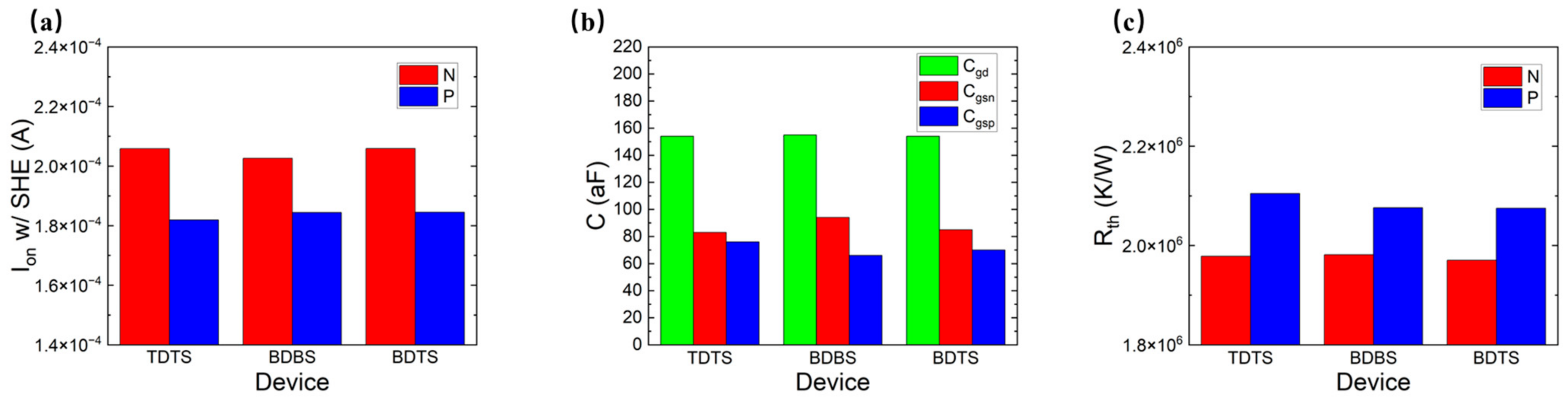
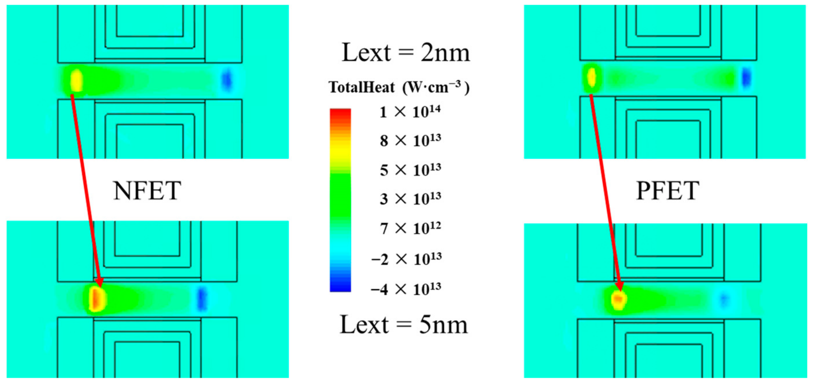
3.1. Buried Thermal Rial

When treating CFET as an inverter and loading a 1 × 10 15   F output capacitance, the time–domain dynamic characteristics of the CFET in response to a square-wave input signal are shown in Figure 4. It is recognized that the channel stress can be boosted to 4.7 Gpa for NS-PFET to increase the PFET’s on-state current ( I o n ) [23]. When the stress of P-channels is 1.4 Gpa, the PFET’s I o n attains 2.48 × 10 4   A , which is the same as that of the NFET. As shown in Figure 4, the high-to-low delay time ( t p h l ) is 2.35 × 10 12   s , which is the same as the low-to-high delay time ( t p l h ).
The max temperature ( T m a x ) and thermal resistance ( R t h ) are important parameters that reflect the electrothermal characteristics of the CFET. T m a x is the highest temperature in the CFET, while R t h is a parameter that reflects the heat dissipation ability, which is calculated by the expression:
R t h = Δ T m a x / I o n × V D D
Because the power of the CFET is mainly generated during the period of charging–discharging, it is important to extract the electrothermal characteristics of both NFET and PFET. Figure 5 shows the method for simulating the electrothermal characteristics. When the input is 1, the gate voltage is swept to 0.7 V. The NFET is on, while the PFET is off. Because the capacitance between the out and the ground is pre-charged, the drain of the NFET is 0.7 V. There is a current through the NFET to discharge the capacitance and generate heat in the NFET until the capacitance is fully discharged. When the input is 0, the gate voltage is swept to 0 V. The NFET is off, while the PFET is on. Because the capacitance between the out and the ground is pre-discharged, the drain of the PFET is 0 V. There is a current through the PFET to charge the capacitance and generate heat in the PFET until the capacitance is fully charged.
Figure 6a–c show three different methods of the CFET, which are the traditional-CFET, the BPR-CFET and the BTR-CFET. Figure 7a,b show the Id-Vg curves of those methods. As the V g s increases, the degradation to I d occurs due to the higher temperature. As the BPR structure provides a heat dissipation path through the device to the bottom, the I d is improved. As the BTR structure provides a shorter heat dissipation path through the device to the bottom, the I d is better improved. Figure 8a–c show the parasitic capacitance between the gate and the drain ( C g d ), the parasitic capacitance between the gate and the source of the NFET ( C g s n ), the parasitic capacitance between the gate and the source of the PFET ( C g s p ), the I o n and the R t h of those methods. The C g s p is higher than the C g s n because of the longer distance of the VDD than that of the VSS, which is obvious in the BPR-CFET and BTR-CFET. The BPR creates another low-thermal-resistance path from the middle to the bottom and decreases the total R t h . Both for the NFET and PFET, the hot spot is much closer to the drain, and the heat flux mainly dissipates through the inner spacer near the drain. For the drain, only one metal via dissipates the heat flux from middle to top, while the thermal resistance between the drain and the bottom is high. Compared with the traditional-CFET, the R t h of the BPR-CFET is reduced by 2% for NFET and 5% for PFET, and its I o n is decreased by 1% for NFET and increased by 5% for PFET.
We propose a BTR technology that creates another low-thermal-resistance path from the drain side to the bottom, decreasing the thermal resistance between the drain and the bottom. Powered by the BTR technology, the R t h of all methods is extremely reduced and the I o n is increased. Compared with the traditional-CFET, the R t h of the BTR-CFET is reduced by 4% for NFET and 9% for PFET, and its I o n is increased by 2% for NFET and 7% for PFET.

3.2. Power Delivery Network

Figure 9a–c show three different methods of the PDN, which are the BTR-TDTS (top-VDD–top-VSS), BTR-BDBS (bottom-VDD–bottom-VSS) and BTR-BDTS (bottom-VDD–top-VSS) with the BTR. Figure 10a–c show the C g d , C g s n , C g s p , I o n and R t h of those methods. The BTR-BDTS makes the difference between the C g s n and C g s p smaller than that of the BTR-BDBS, which provides the potential for capacitor matching. Powered by the BTR, all cases are improved on the I o n and the R t h for the NFET and the PFET. Compared with the BTR-TDTS, the R t h of the BTR-BDBS is almost the same for NFET and is decreased by 2% for PFET, and its I o n is decreased by 2% for NFET and increased by 2% for PFET.
Because a low-thermal-resistance path from the middle to the bottom is created by the BTR, two low-thermal-resistance paths from the middle to the top created by the VDD and the VSS appear superfluous in the BTR-BDBS. The BDTS creates another low-thermal-resistance path from the middle to the top. Compared with the BTR-TDTS, the R t h of the BTR-BDTS is decreased by 1% for NFET and 2% for PFET, and its I o n is almost the same for NFET and increased by 2% for PFET. Compared with the traditional-TDTS, the R t h of the BTR-BDTS is decreased by 5% for NFET and 9% for PFET, and its I o n is increased by 2% for NFET and 7% for PFET.

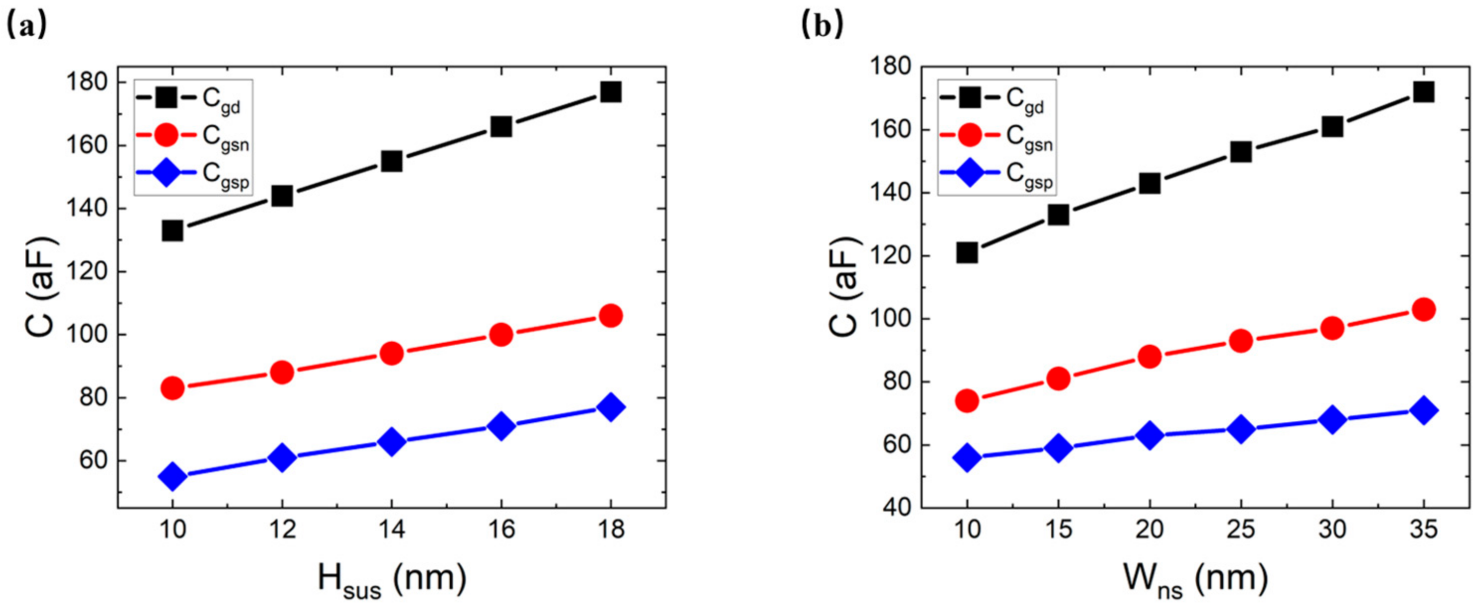
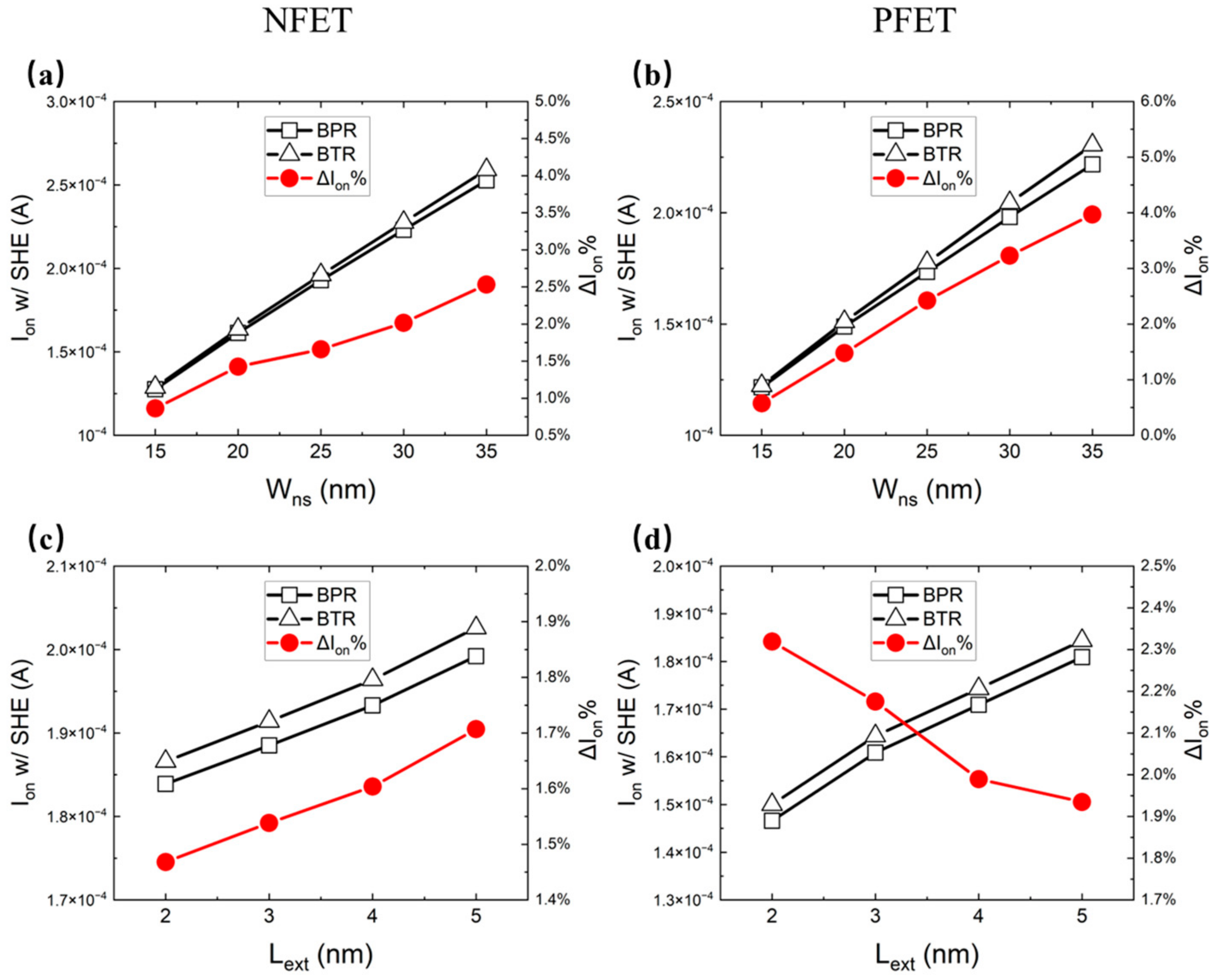
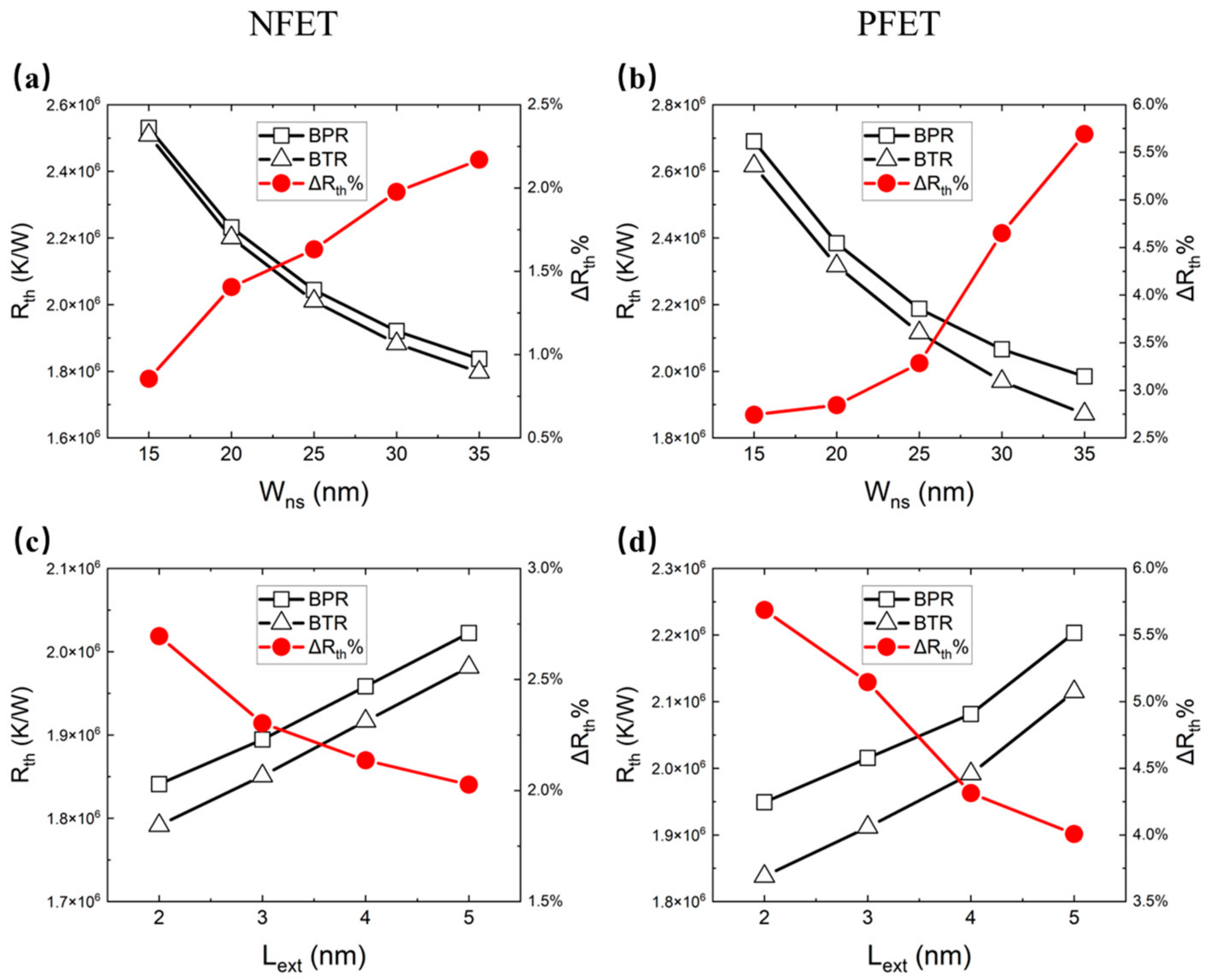
3.3. Characteristics of CFET for Different Dimension Parameters

To further study the electrothermal characteristics, the C g d , C g s n , C g s p , I o n , Δ I o n % , R t h and Δ R t h % of the CFET with different parameters were extracted. Δ I o n % is a parameter that reflects the variation in current caused by BTR, which is calculated by the expression:
Δ I o n % = I o n ,   B T R I o n ,   B P R × 100 %
Δ R t h % is a parameter that reflects the variation in thermal resistance caused by BTR, which is calculated by the expression:
Δ R t h % = R t h ,   B T R R t h ,   B P R × 100 %
Figure 11a,b show the C g d , C g s n and C g s p for different values of the channel suspension height ( H s u s ) and nanosheet width ( W n s ). The increment in the H s u s increases the C g d , C g s n and C g s p because the increment in the H s u s extends the gate size in the vertical direction. The increment in the W n s increases the C g d , C g s n and C g s p because the extension of the gate size in the lateral direction increases the area of the capacitance plate.
Figure 12a–d show the I o n with SHE and the Δ I o n % for different values of the W n s and extension doping length ( L e x t ) between the BTR and BPR. The increment in the W n s and L e x t increases the I o n due to the extension of the effect channel width and the decrement in the channel resistance. The BTR shows more advantages for the I o n than the BPR both for the NFET and PFET. When the W n s increases, the Δ I o n % increases because of the larger thermal conductivity area. When the L e x t increases, the Δ I o n % of the NFET increases. This is because the Δ I o n / Δ T is larger at high temperatures. When the L e x t increases, the Δ I o n % of the PFET decreases. This is because a lower L e x t contributes more to decreasing the temperature.
Figure 13a–d show the R t h and Δ R t h % for different values of W n s and L e x t between the BTR and BPR. The increment in the W n s lowers the R t h because of the extension of the channel’s heat dissipation area. The increment in the L e x t strongly increases the R t h because of the variation in the hot spot, which increases the heat dissipation path in the high thermal resistance channel, as shown in Figure 14. When the W n s increases, the Δ R t h % increases because of the larger thermal conductivity area. When the L e x t increases, the Δ R t h % of the NFET decreases. This is because the hot spot is further away from the BTR.

4. Conclusions

For the first time, BTR technology is proposed and is shown by a process flow. Different methods of CFET are compared in terms of electrothermal characteristics and parasitic capacitance. Powered by BTR technology, the R t h of all methods is extremely reduced, and the I o n is increased. Compared with the traditional-CFET, the R t h of the BTR-CFET is reduced by 4% for NFET and 9% for PFET, and its I o n is increased by 2% for NFET and 7% for PFET. A comparison between different PDN methods with a buried thermal rail (BTR) reveals the performance advantage of the CFET architecture. Compared with the BTR-TDTS, the R t h of the BTR-BDTS is decreased by 1% for NFET and 2% for PFET, and its I o n is almost the same for NFET and increased by 2% for PFET. Here, the influence of different parameters, such as C g d , C g s n , C g s p , I o n , Δ I o n % , R t h and Δ R t h % , on the CFET is well studied. The increment in H s u s and W n s increases the C g d , C g s n and C g s p . The increment in W n s and L e x t increases the I o n because of the extension of the effect channel width and the decrement in channel resistance. The increment in the W n s decreases the R t h because of the extension of the channel’s heat dissipation area. The increment in the L e x t significantly increases the R t h because of the variation in the hot spot, which increases the heat dissipation path in the high thermal resistance channel.

Author Contributions

Conceptualization, Z.P. and T.L.; methodology, Z.P. and T.L.; software, Z.P. and K.C.; validation, Z.P.; formal analysis, Z.P. and T.L.; investigation, Z.P. and J.Y.; resources, S.X. and C.W.; data curation, Z.P.; writing—original draft preparation, Z.P.; writing—review and editing, T.L. and M.X.; visualization, Z.P. and T.L.; supervision, T.L., M.X. and D.W.Z.; project administration, M.X.; funding acquisition, M.X. and D.W.Z. All authors have read and agreed to the published version of the manuscript.

Funding

This research was funded by a platform for the development of next-generation integrated circuit technology and the Shanghai Sailing Program, 21YF1402700.

Data Availability Statement

The data that support the findings of this study are available from the corresponding author upon reasonable request.

Conflicts of Interest

The authors declare no conflict of interest.

References

  1. IEEE International Roadmap for Devices and Systems (IRDS™) 2022 Edition. Available online: https://irds.ieee.org/editions/2022 (accessed on 30 December 2022).
  2. Yoon, J.-S.; Baek, R.-H. Device Design Guideline of 5-nm-Node FinFETs and Nanosheet FETs for Analog/RF Applications. IEEE Access 2020, 8, 189395–189403. [Google Scholar] [CrossRef]
  3. Yakimets, D.; Bardon, M.G.; Jang, D.; Schuddinck, P.; Sherazi, Y.; Weckx, P.; Miyaguchi, K.; Parvais, B.; Raghavan, P.; Spessot, A.; et al. Power aware FinFET and lateral nanosheet FET targeting for 3 nm CMOS technology. In Proceedings of the 2017 IEEE International Electron Devices Meeting (IEDM), San Francisco, CA, USA, 2–6 December 2017; pp. 20.4.1–20.4.4. [Google Scholar] [CrossRef]
  4. Bardon, M.G.; Sherazi, Y.; Jang, D.; Yakimets, D.; Schuddinck, P.; Baert, R.; Mertens, H.; Mattii, L.; Parvais, B.; Mocuta, A.; et al. Power-performance Trade-offs for Lateral NanoSheets on Ultra-Scaled Standard Cells. In Proceedings of the 2018 IEEE Symposium on VLSI Technology, Honolulu, HI, USA, 18–22 June 2018; pp. 143–144. [Google Scholar] [CrossRef]
  5. Chang, S.-W.; Huang, M.-K.; Huang, S.-T.; Wang, H.-C.; Wang, J.-Y.; Yu, L.-W.; Huang, Y.-F.; Hsueh, F.-K.; Sung, P.-J.; Wu, C.-T.; et al. First Demonstration of CMOS Inverter and 6T-SRAM Based on GAA CFETs Structure for 3D-IC Applications. In Proceedings of the 2019 IEEE International Electron Devices Meeting (IEDM), San Francisco, CA, USA, 7–11 December 2019; pp. 11.7.1–11.7.4. [Google Scholar] [CrossRef]
  6. Ryckaert, J.; Schuddinck, P.; Weckx, P.; Bouche, G.; Vincent, B.; Smith, J.; Sherazi, Y.; Mallik, A.; Mertens, H.; Demuynck, S.; et al. The Complementary FET (CFET) for CMOS scaling beyond N3. In Proceedings of the 2018 IEEE Symposium on VLSI Technology, Honolulu, HI, USA, 18–22 June 2018; pp. 141–142. [Google Scholar] [CrossRef]
  7. Huang, C.-Y.; Dewey, G.; Mannebach, E.; Phan, A.; Morrow, P.; Rachmady, W.; Tung, I.-C.; Thomas, N.; Alaan, U.; Paul, R.; et al. 3-D Self-aligned Stacked NMOS-on-PMOS Nanoribbon Transistors for Continued Moore’s Law Scaling. In Proceedings of the 2020 IEEE International Electron Devices Meeting (IEDM), San Francisco, CA, USA, 12–18 December 2020; pp. 20.6.1–20.6.4. [Google Scholar] [CrossRef]
  8. Jiang, L.; Pal, A.; Bazizi, E.M.; Saremi, M.; Ren, H.; Alexander, B.; Ayyagari-Sangamalli, B. Complementary FET Device and Circuit Level Evaluation Using Fin-Based and Sheet-Based Configurations Targeting 3nm Node and Beyond. In Proceedings of the 2020 International Conference on Simulation of Semiconductor Processes and Devices (SISPAD), Kobe, Japan, 23 September–6 October 2020; pp. 323–326. [Google Scholar] [CrossRef]
  9. Jung, S.-G.; Jang, D.; Min, S.-J.; Park, E.; Yu, H.-Y. Performance Analysis on Complementary FET (CFET) Relative to Standard CMOS With Nanosheet FET. IEEE J. Electron Devices Soc. 2022, 10, 78–82. [Google Scholar] [CrossRef]
  10. Sun, B.; Xu, Z.; Ding, R.; Yang, J.; Chen, K.; Xu, S.; Xu, M.; Lu, Y.; Zhu, X.; Yu, S.; et al. Analytical Model of CFET Parasitic Capacitance for Advanced Technology Nodes. IEEE Trans. Electron Devices 2022, 69, 936–941. [Google Scholar] [CrossRef]
  11. Yang, X.; Sun, Y.; Liu, Z.; Liu, Y.; Li, X.; Shi, Y. 3-D Modeling of Fringe Gate Capacitance in Complementary FET (CFET). IEEE Trans. Electron Devices 2022, 69, 5978–5984. [Google Scholar] [CrossRef]
  12. Myeong, I.; Song, I.; Kang, M.J.; Shin, H. Self-Heating and Electrothermal Properties of Advanced Sub-5-nm Node Nanoplate FET. IEEE Electron Device Lett. 2020, 41, 977–980. [Google Scholar] [CrossRef]
  13. Bury, E.; Kaczer, B.; Linten, D.; Witters, L.; Mertens, H.; Waldron, N.; Zhou, X.; Collaert, N.; Horiguchi, N.; Spessot, A.; et al. Self-heating in FinFET and GAA-NW using Si, Ge and III/V channels. In Proceedings of the 2016 IEEE International Electron Devices Meeting (IEDM), San Francisco, CA, USA, 3–7 December 2016; pp. 15.6.1–15.6.4. [Google Scholar] [CrossRef]
  14. Takahashi, T.; Beppu, N.; Chen, K.; Oda, S.; Uchida, K. Thermal-aware device design of nanoscale bulk/SOI FinFETs: Suppression of operation temperature and its variability. In Proceedings of the 2011 International Electron Devices Meeting, Washington, DC, USA, 5–7 December 2011; pp. 34.6.1–34.6.4. [Google Scholar] [CrossRef]
  15. Jung, S.-G.; Jang, D.; Min, S.-J.; Park, E.; Yu, H.-Y. Device Design Guidelines of 3-nm Node Complementary FET (CFET) in Perspective of Electrothermal Characteristics. IEEE Access 2022, 10, 41112–41118. [Google Scholar] [CrossRef]
  16. Zhao, S.; Cai, L.; Chen, W.; He, Y.; Du, G. Self-Heating and Thermal Network Model for Complementary FET. IEEE Trans. Electron Devices 2021, 69, 11–16. [Google Scholar] [CrossRef]
  17. Prasad, D.; Nibhanupudi, S.S.T.; Das, S.; Zografos, O.; Chehab, B.; Sarkar, S.; Baert, R.; Robinson, A.; Gupta, A.; Spessot, A.; et al. Buried Power Rails and Back-side Power Grids: Arm® CPU Power Delivery Network Design beyond 5 nm. In Proceedings of the 2019 IEEE International Electron Devices Meeting (IEDM), San Francisco, CA, USA, 7–11 December 2019; pp. 19.1.1–19.1.4. [Google Scholar] [CrossRef]
  18. Subramanian, S.; Hosseini, M.; Chiarella, T.; Sarkar, S.; Schuddinck, P.; Chan, B.T.; Radisic, D.; Mannaert, G.; Hikavyy, A.; Rosseel, E.; et al. First Monolithic Integration of 3D Complementary FET (CFET) on 300 mm Wafers. In Proceedings of the 2020 IEEE Symposium on VLSI Technology, Honolulu, HI, USA, 16–19 June 2020; pp. 1–2. [Google Scholar] [CrossRef]
  19. Schuddinck, P.; Zografos, O.; Weckx, P.; Matagne, P.; Sarkar, S.; Sherazi, Y.; Baert, R.; Jang, D.; Yakimets, D.; Gupta, A.; et al. Device-, Circuit- & Block-level evaluation of CFET in a 4 track library. In Proceedings of the 2019 Symposium on VLSI Technology, Kyoto, Japan, 9–14 June 2019; pp. T204–T205. [Google Scholar] [CrossRef]
  20. Liu, W.; Etessam-Yazdani, K.; Hussin, R.; Asheghi, M. Modeling and Data for Thermal Conductivity of Ultrathin Single-Crystal SOI Layers at High Temperature. IEEE Trans. Electron Devices 2006, 53, 1868–1876. [Google Scholar] [CrossRef]
  21. Yan, J.-Y.; Jan, S.-R.; Peng, Y.-J.; Lin, H.H.; Wan, W.K.; Huang, Y.-H.; Hung, B.; Chan, K.-T.; Huang, M.; Yang, M.-T.; et al. Thermal resistance modeling of back-end interconnect and intrinsic FinFETs, and transient simulation of inverters with capacitive loading effects. In Proceedings of the 2016 IEEE International Electron Devices Meeting (IEDM), San Francisco, CA, USA, 3–7 December 2016; pp. 35.6.1–35.6.4. [Google Scholar] [CrossRef]
  22. Pop, E.; Dutton, R.; Goodson, K. Thermal analysis of ultra-thin body device scaling [SOI and FinFet devices]. In Proceedings of the IEEE International Electron Devices Meeting 2003, Washington, DC, USA, 8–10 December 2003; pp. 36.6.1–36.6.4. [Google Scholar] [CrossRef]
  23. Liu, T.; Wang, D.; Pan, Z.; Chen, K.; Yang, J.; Wu, C.; Xu, S.; Wang, C.; Xu, M.; Zhang, D.W. Novel Postgate Single Diffusion Break Integration in Gate-All-Around Nanosheet Transistors to Achieve Remarkable Channel Stress for N/P Current Matching. IEEE Trans. Electron Devices 2022, 69, 1497–1502. [Google Scholar] [CrossRef]
Figure 1. (a) Three-dimensional view of the CFET; (b) CFET cross-sectional view through the channel; (c) schematic of structural parameters of CFET in cross-sectional view.
Micromachines 14 01751 g001
Figure 2. Calibrated curves of double-fin-based CFET between experimental reference and TCAD simulation and curves of double-fin-based CFET with self-heating effect (SHE): (a) Id-Vgs; (b) gm-Vgs and gm/Id-Vgs for the NFET; (c) gm-Vgs and gm/Id-Vgs for the PFET; (d) gm-Vgs and gm/Id-Vgs for the NFET with SHE; (e) gm-Vgs and gm/Id-Vgs for the PFET with SHE. (Reference_N means the reference data of the NFET, TCAD_N means the TCAD simulation result of the NFET, SHE_N means the TCAD simulation result of the NFET with self-heating effect, and the same applies to the PFET).
Micromachines 14 01751 g002
Figure 3. CFET process flow: (a) NS Mandrel; (b) STI and BPR; (c) Dummy Gate; (d) BDI (bottom dielectric insulator) and MDI (middle dielectric insulator); (e) Inner Spacer; (f) BTR; (g) Bottom Epi and Contact; (h) Top Epi and Contact; (i) Dummy Gate Removal; (j) RMG (replaced metal gate); (k) BEOL (back-end-of-line).
Micromachines 14 01751 g003
Figure 4. The time–domain dynamic characteristics of the CFET in response to a square-wave input signal.
Micromachines 14 01751 g004
Figure 5. Schematic of the simulation of electrothermal characteristics.
Micromachines 14 01751 g005
Figure 6. Three CFET structures: (a) traditional-CFET, (b) BPR-CFET, and (c) BTR-CFET.
Micromachines 14 01751 g006
Figure 7. The Id-Vg curves of these methods: (a) NFET and (b) PFET.
Micromachines 14 01751 g007
Figure 8. (a) The I o n ; (b) C g d , C g s n , and C g s p ; and (c) R t h of different methods of the CFET.
Micromachines 14 01751 g008
Figure 9. Power delivery structures based on the BTR process: (a) BTR-TDTS, (b) BTR-BDBS, and (c) BTR-BDTS.
Micromachines 14 01751 g009
Figure 10. (a) The I o n , (b) the C g d , the C g s n , the C g s p and (c) the R t h of different methods of PDN.
Micromachines 14 01751 g010
Figure 11. The C g d , C g s n and C g s p for different values of (a) H s u s and (b) W n s .
Micromachines 14 01751 g011
Figure 12. The I o n with SHE and the Δ I o n % of the NFET for different values of (a) W n s and (c) L e x t , and those of the PFET for different values of (b) W n s and (d) L e x t .
Micromachines 14 01751 g012
Figure 13. The R t h and Δ R t h % of the NFET for different values of (a) W n s and (c) L e x t , and those of the PFET for different values of (b) W n s and (d) L e x t .
Micromachines 14 01751 g013
Figure 14. Red arrows show the variation in the hot spot, depending on the L e x t .
Micromachines 14 01751 g014
Table 1. Structural and electrical parameters of the CFET.
SymbolQuantityValues
L g Gate length12 nm
H c h Channel height5 nm
H s u s Suspension height14 nm
T H f O 2 Gate HfO 2 thickness1.5 nm
T S i O 2 Gate SiO 2 thickness0.5 nm
L s p Spacer length5 nm
C D B P R CD of BPR36 nm
H B P R Height of BPR90 nm
D B P R Buried depth of BPR23 nm
H M D I Height of MDI20 nm
D S T I STI depth70 nm
M 0 Metal 0 pitch21 nm
M 1 Metal 1 pitch42 nm
N c h n N-channel doping concentration 1 × 10 15   cm 3
N c h p P-channel doping concentration 1 × 10 18   cm 3
N s d S/D epitaxy doping concentration 1 × 10 21   cm 3
N e x t Extension doping concentration 1 × 10 20 cm 3
R s d S/D contact resistivity 1 × 10 9   Ω · cm 2
S D n NFET S/D materialSi
S D p PFET S/D materialSiGe (75% Ge)
S t r e s s p P-channel stress0.8 Gpa
Table 2. Thermal parameters of the CFET.
Thermal Conductivity Values   W / K · m
Oxide1.4
Tungsten175
Nitride18.5
HfO 2 2.3
Substrate148
Channel7.5
S/D (Si)5.5
S/D (SiGe)1.0
Thermal Contact Resistance Values   c m 2 · K / W
Si / HfO 2 2 × 10 4
Top 4 × 10 5
Bottom 4 × 10 5
Environment Temperature300 K
Disclaimer/Publisher’s Note: The statements, opinions and data contained in all publications are solely those of the individual author(s) and contributor(s) and not of MDPI and/or the editor(s). MDPI and/or the editor(s) disclaim responsibility for any injury to people or property resulting from any ideas, methods, instructions or products referred to in the content.

