
Structural Optimization Design of Microfluidic Chips Based on Fast Sequence Pair Algorithm
 , , and
Abstract
:1. Introduction
2. Structure Optimization of a Microfluidic Chip
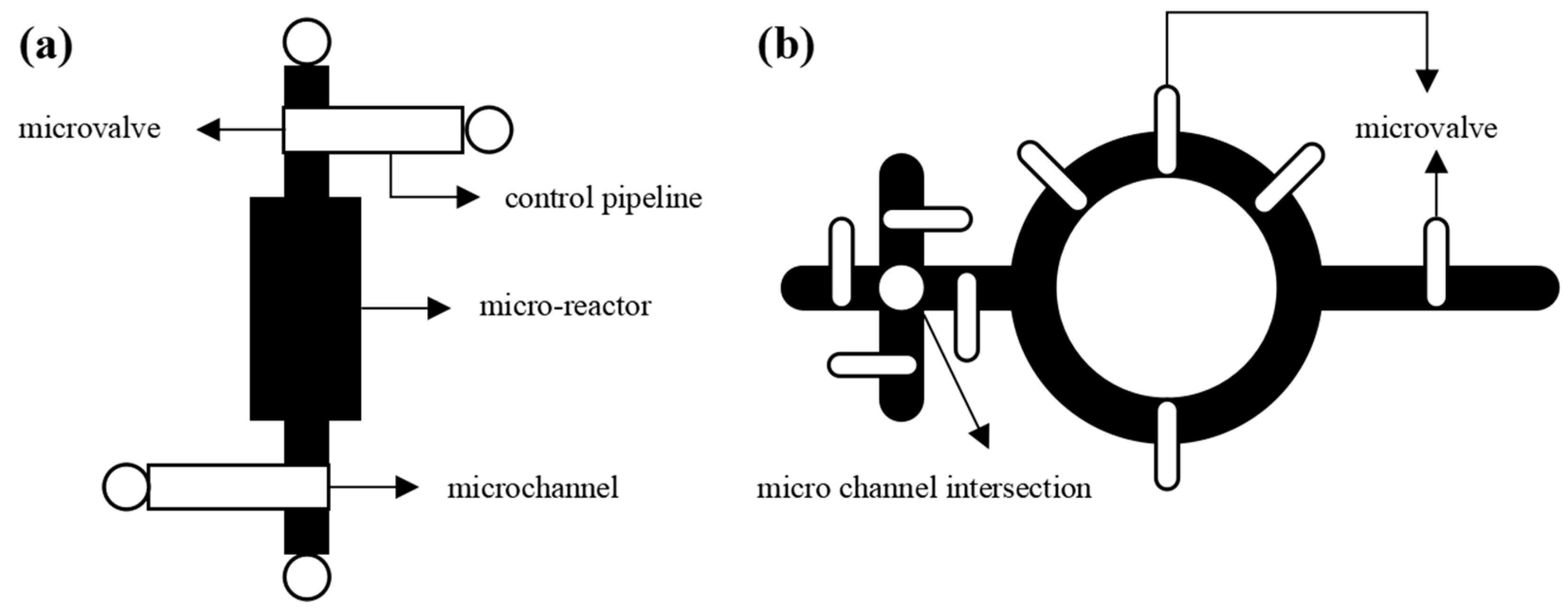
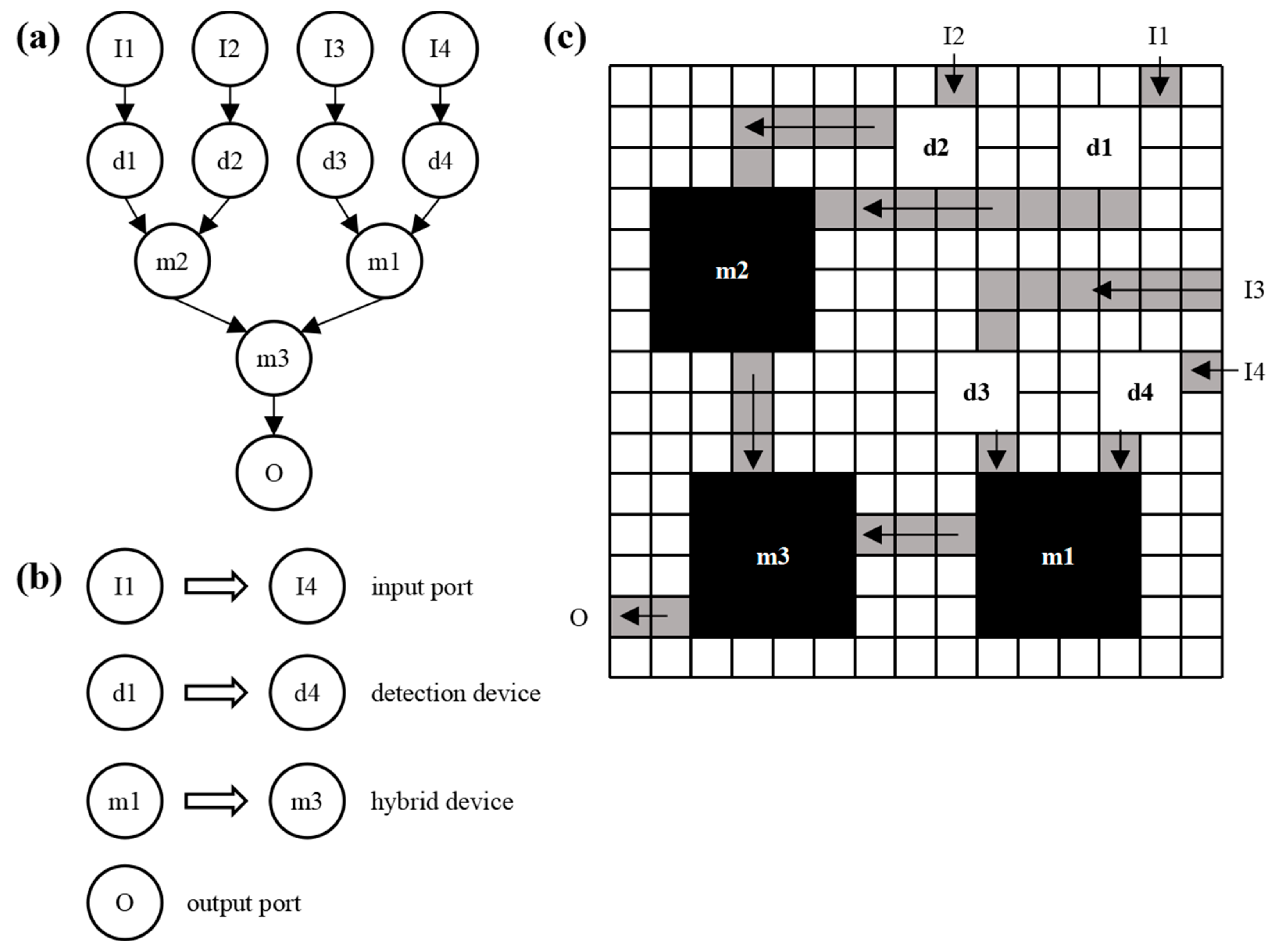
2.1. Structural Modeling of Microfluidic Chips
- Definition of a structural optimization problem
- 2.
- Structural design modeling
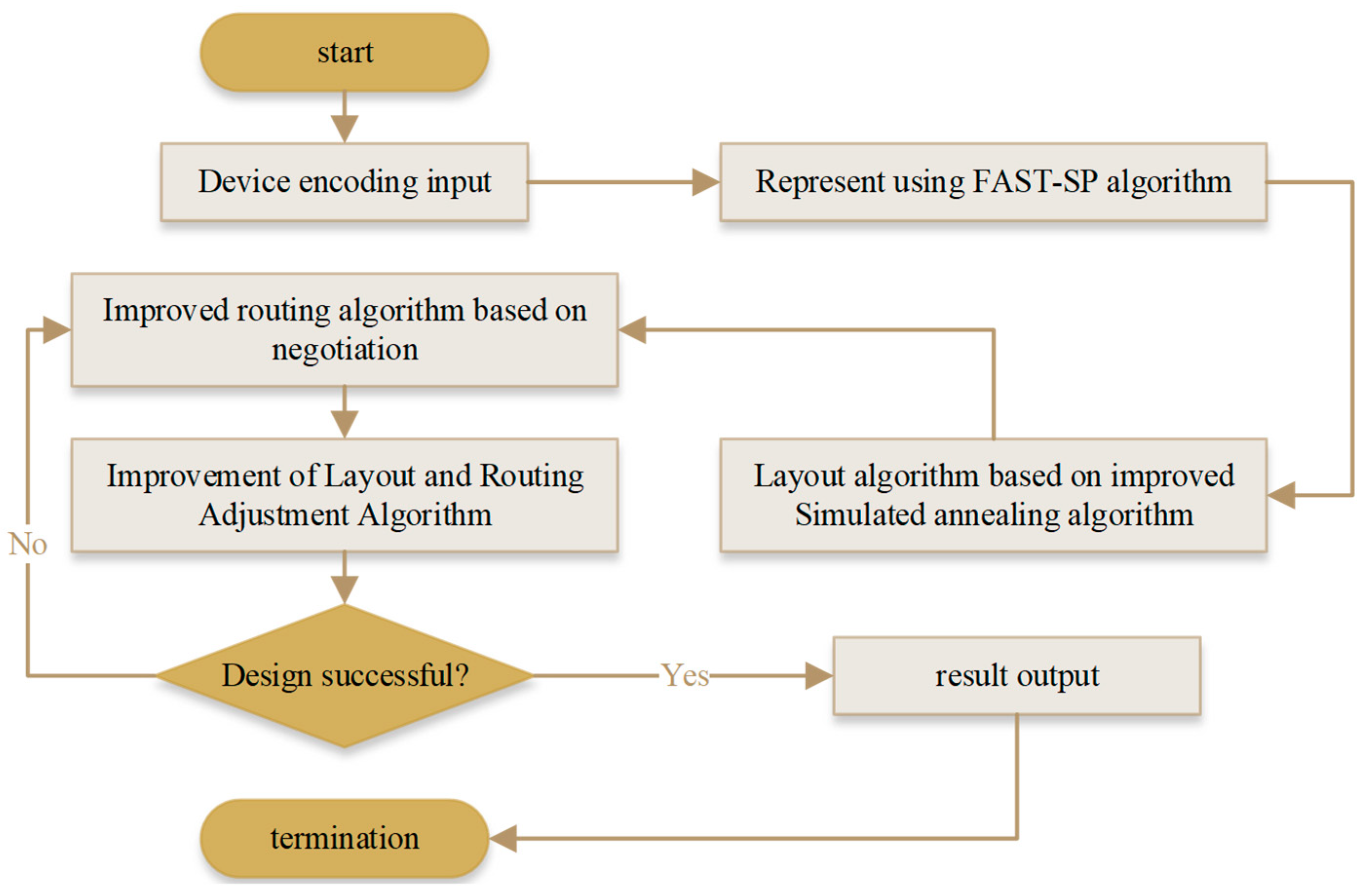
2.2. Algorithm Design
- (1)
- Calculate the weighted LCS width of two sequences, S1 and S2, and use the vector block order to record the index of each device in S2.
- (2)
- Initialize vector lengths to 0 to store each device’s maximum quantity (length or width).
- (3)
- The variable block is defined as the current device in S1, and the index is the index of the current device in S2. All the items on the left of the block are arranged into intervals with the length of the block, and the block is then placed.
- (4)
- The total length of the updated layout is length, and length [n] indicates the full length after n devices are determined.
- (5)
- It is updated if the length [j] exceeds the current length.
2.3. Layout Calculation Optimization
- (1)
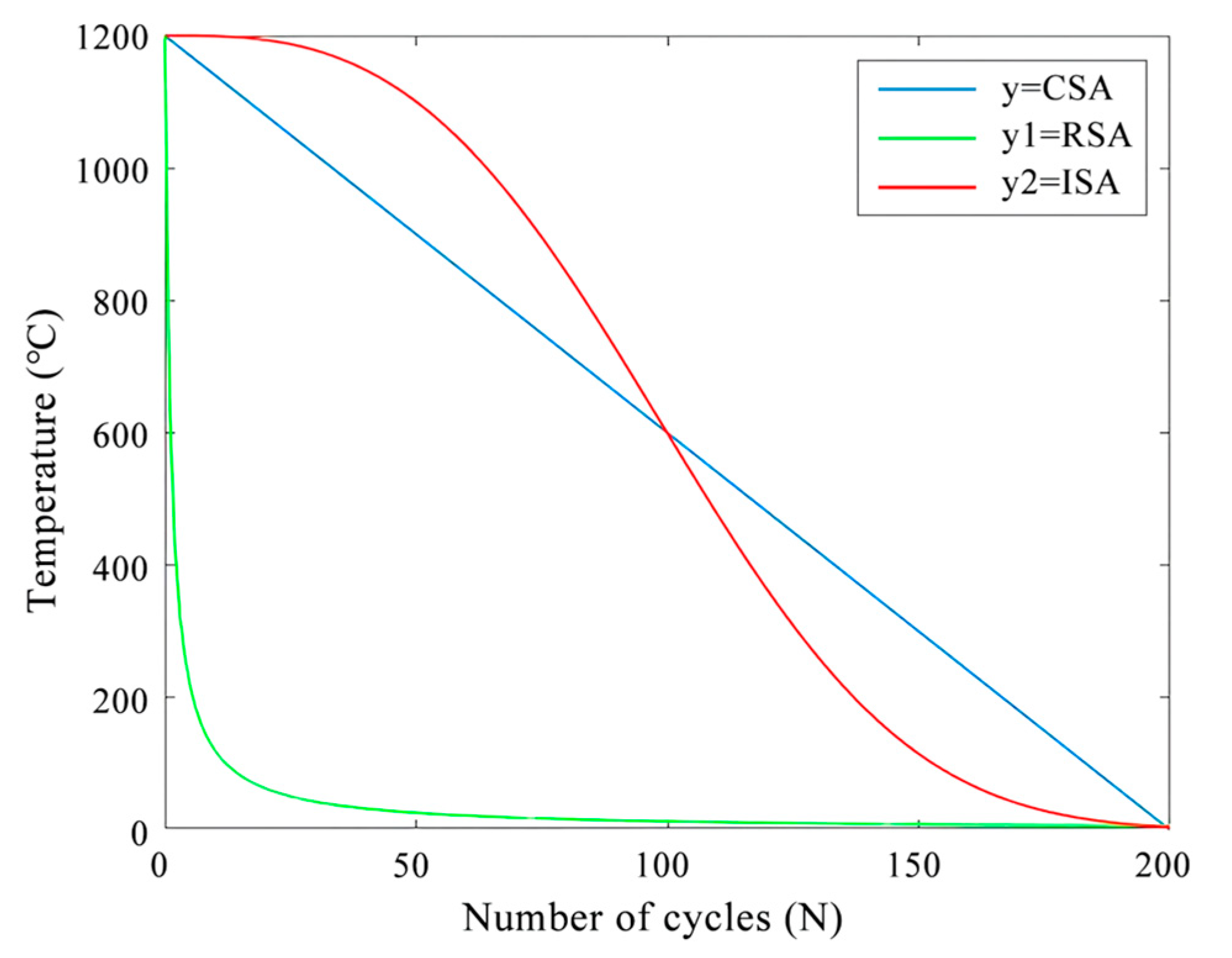
- Change of algorithm cooling function
- (1)
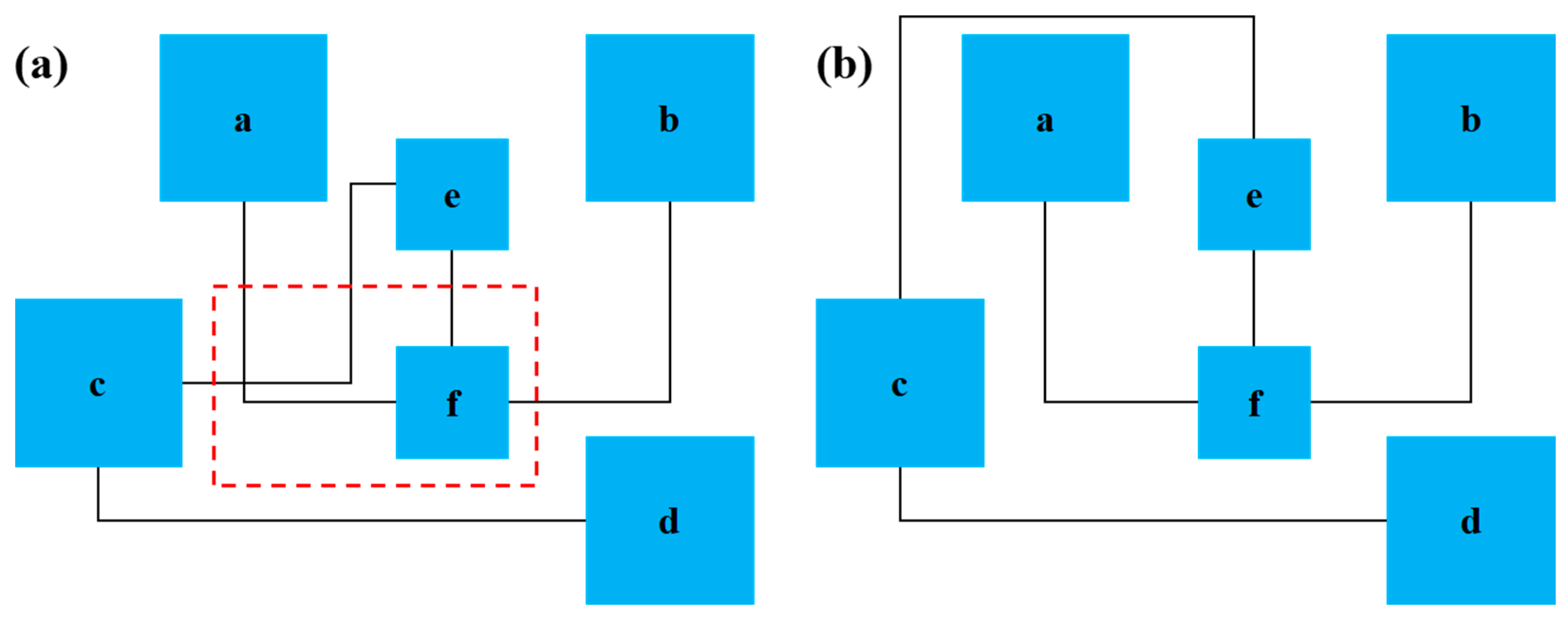
- Use reverse transformation to select two device units and reverse all units between the two units.
- (2)
- Select three device units and switch the unit between the two device units to the back of the third unit.
- (2)
- Change of algorithmic search strategy
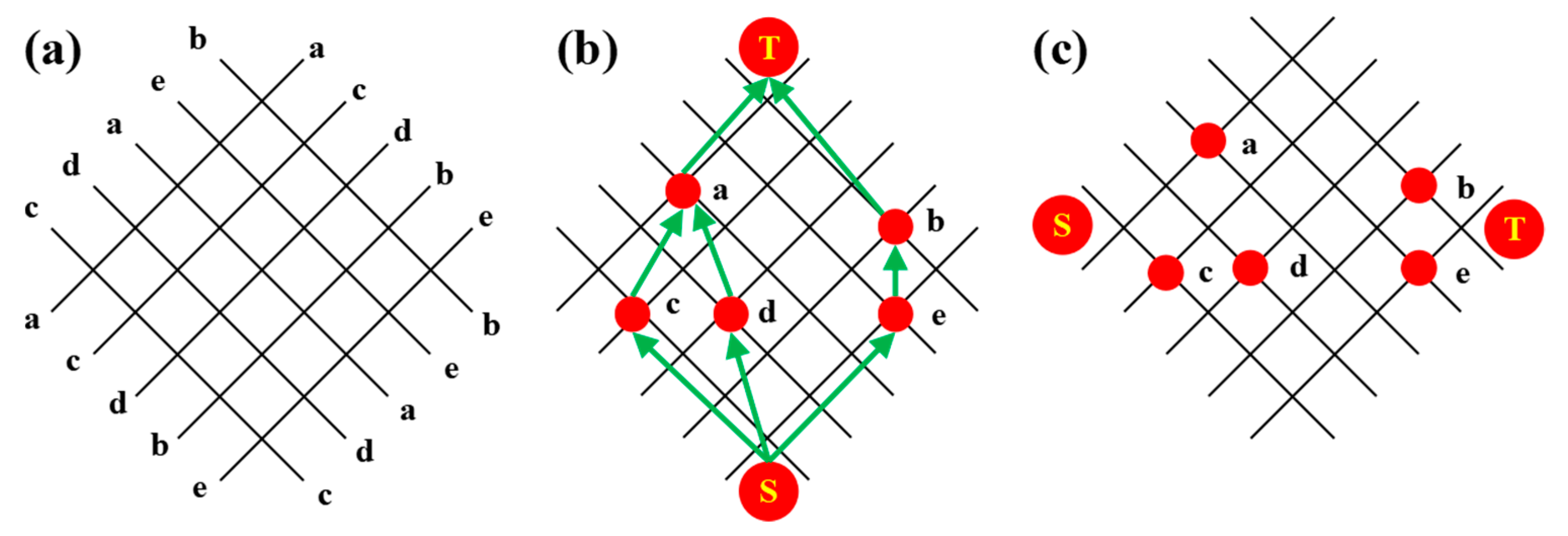
2.4. Routing Algorithm Optimization
2.5. Adjustment Algorithm Optimization
2.6. Improved Algorithm Flow
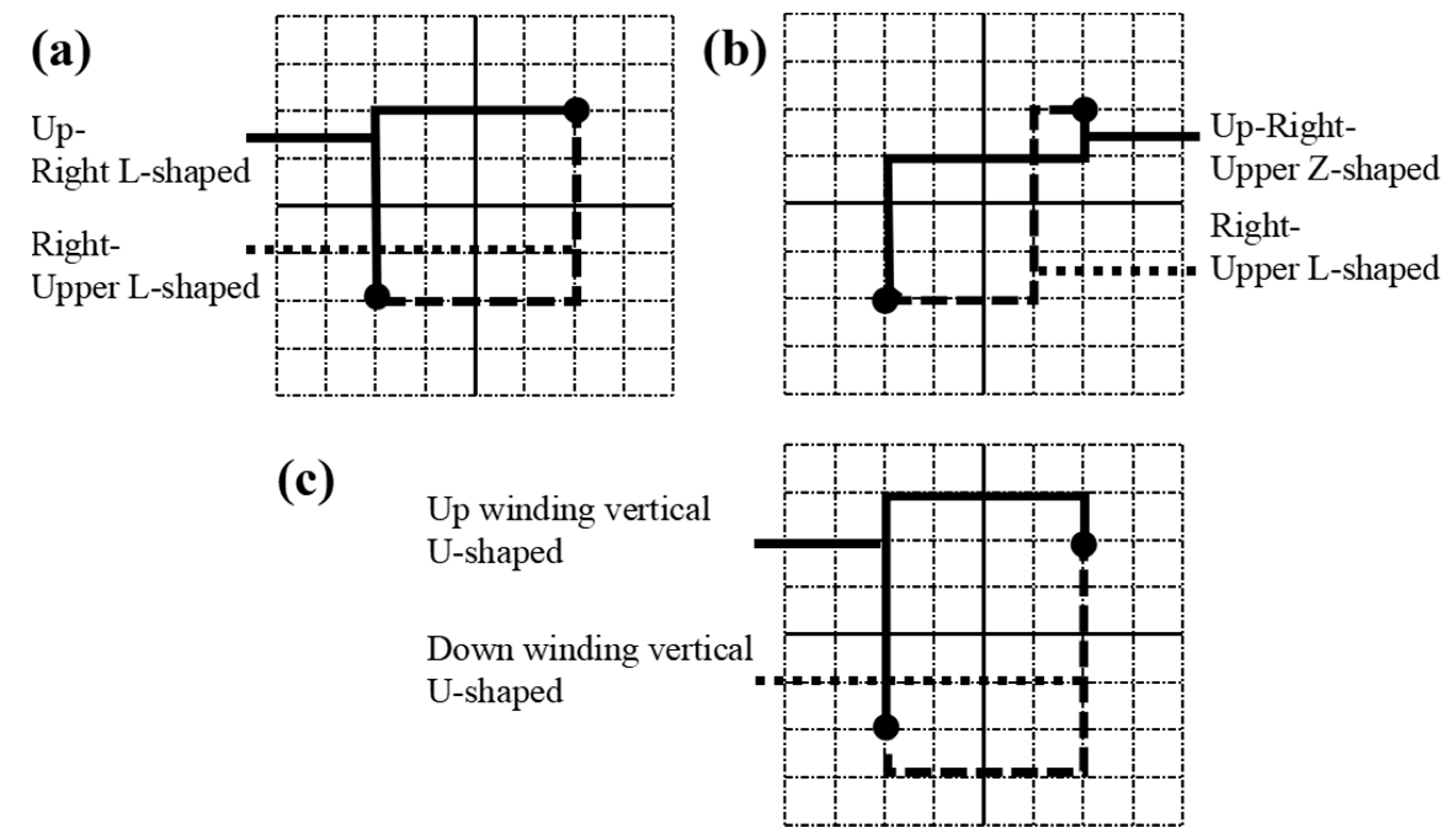
- The distance between device mi and device mj on its right or above is defined as rx and axe.
- The width and height of all device set spacing are defined as WX and WY. The constraint condition of elements between WX and WY is [emin, emax]. WX and WY form the initial solution S.
- In the simulated annealing algorithm, the initial temperature is defined as T, the number of external cycles is N, the end temperature is Tend, the current temperature is T0, the chain length is L, and the quality function for evaluating the chip layout is E (S).
- (1)
- Initialize WX and HY: emin < rx, rx < emax.
- (2)
- Set the state variables S = (SX, SY, WX, HY) and the initial temperature T. When the initial test temperature exceeds the minimum temperature, the iteration starts.
- (3)
- Adjust the state variable S -> S1, randomly generate the variables rx1 and ax1, and compare them with emin and emax. When rx1 < emin, let emin = rx1; when rx1 > emax, let emin = rx1. The ax1 is obtained in the same way.
- (4)
- (5)
- Cool down. Use the new cooling rate function to cool down. Stop iterating and output the current result if T0 exceeds the end temperature.
- ①
- Non-negative edge weight graph G (WX, HY).
- ②
- A starting source node s.
- ③
- One target end node t.
3. Experimental Results and Analysis
4. Conclusions
Author Contributions
Funding
Data Availability Statement
Conflicts of Interest
References
- Yin, B.; Yue, W.; Sohan, A.; Zhou, T.; Qian, C.; Wan, X. Micromixer with Fine-Tuned Mathematical Spiral Structures. ACS Omega 2021, 6, 30779–30789. [Google Scholar] [CrossRef]
- Yin, B.; Wan, X.; Qian, C.; Sohan, A.; Wang, S.; Zhou, T. Point-of-Care Testing for Multiple Cardiac Markers Based on a Snail-Shaped Microfluidic Chip. Front. Chem. 2021, 9, 741058. [Google Scholar] [CrossRef]
- Li, R.; Wei, X.; Xu, J.; Chen, J.; Li, B.; Wu, Z.; Wang, Z.L. Smart Wearable Sensors Based on Triboelectric Nanogenerator for Personal Healthcare Monitoring. Micromachines 2021, 12, 352. [Google Scholar] [CrossRef]
- Yin, B.F.; Wan, X.H.; Yang, M.Z.; Qian, C.C.; Sohan, A. Wave-shaped microfluidic chip assisted point-of-care testing for accurate and rapid diagnosis of infections. Mil. Med. Res. 2022, 9, 8–21. [Google Scholar] [CrossRef]
- Yin, B.; Qian, C.; Wan, X.; Muhtasim Fuad Sohan, A.S.M.; Lin, X. Tape integrated self-designed microfluidic chip for point-of-care immunoassays simultaneous detection of disease biomarkers with tunable detection range. Biosens. Bioelectron. 2022, 212, 114429. [Google Scholar] [CrossRef]
- Yin, B.; Wan, X.; Qian, C.; Sohan, A.; Zhou, T.; Yue, W. Enzyme Method-Based Microfluidic Chip for the Rapid Detection of Copper Ions. Micromachines 2021, 12, 1380. [Google Scholar] [CrossRef]
- Shin, W.; Kim, H.J. 3D in vitro morphogenesis of human intestinal epithelium in a gut-on-a-chip or a hybrid chip with a cell culture insert. Nat. Protoc. 2022, 17, 910–939. [Google Scholar] [CrossRef]
- Zhang, Y.; Tseng, T.M.; Schlichtmann, U. Portable all-in-one automated microfluidic system (PAMICON) with 3D-printed chip using novel fluid control mechanism. Sci. Rep. 2021, 11, 19189–19199. [Google Scholar] [CrossRef]
- Aishan, Y.; Funano, S.I.; Sato, A.; Ito, Y.; Ota, N.; Yalikun, Y.; Tanaka, Y. Bio-actuated microvalve in microfluidics using sensing and actuating function of Mimosa pudica. Sci. Rep. 2022, 12, 7653–7664. [Google Scholar] [CrossRef]
- Gong, J.; Wang, Q.; Liu, B.; Zhang, H.; Gui, L. A Novel On-Chip Liquid-Metal-Enabled Microvalve. Micromachines 2021, 12, 1051. [Google Scholar] [CrossRef]
- Im, S.B.; Uddin, M.J.; Jin, G.J.; Shim, J.S. A disposable on-chip microvalve and pump for programmable microfluidics. Lab. A Chip 2018, 18, 1310–1319. [Google Scholar] [CrossRef]
- Liu, W.; He, H.; Zheng, S.Y. Microfluidics in Single-Cell Virology: Technologies and Applications. Trends Biotechnol. 2020, 38, 1360–1372. [Google Scholar] [CrossRef]
- Peshin, S.; Madou, M.; Kulinsky, L. Microvalves for Applications in Centrifugal Microfluidics. Sensors 2022, 22, 8955. [Google Scholar] [CrossRef]
- Hayes, B.; Smith, L.; Kabutz, H.; Hayes, A.C.; Whiting, G.L.; Jayaram, K.; MacCurdy, R. Rapid Fabrication of Low-Cost Thermal Bubble-Driven Micro-Pumps. Micromachines 2022, 13, 1634. [Google Scholar] [CrossRef]
- Gao, R.Z.; Hébert, M.; Huissoon, J.; Ren, C.L. µPump: An open-source pressure pump for precision fluid handling in microfluidics. HardwareX 2020, 7, e00096. [Google Scholar] [CrossRef]
- Bao, Q.; Zhang, J.; Tang, M.; Huang, Z.; Lai, L.; Huang, J.; Wu, C. A Novel PZT Pump with Built-in Compliant Structures. Sensors 2019, 19, 1301. [Google Scholar] [CrossRef] [Green Version]
- Tang, P.C.; Eriksson, O.; Sjögren, J.; Fatsis-Kavalopoulos, N.; Kreuger, J.; Andersson, D.I. A Microfluidic Chip for Studies of the Dynamics of Antibiotic Resistance Selection in Bacterial Biofilms. Front. Cell. Infect. Microbiol. 2022, 12, 896149. [Google Scholar] [CrossRef]
- Reyes, D.R.; van Heeren, H. Proceedings of the First Workshop on Standards for Microfluidics. J. Res. Natl. Inst. Stand. Technol. 2019, 124, 1–22. [Google Scholar] [CrossRef]
- Tian, L.L.; Li, C.H.; Ye, Q.C.; Li, Y.F.; Huang, C.Z.; Zhan, L.; Wang, D.M.; Zhen, S.J. A centrifugal microfluidic chip for point-of-care testing of staphylococcal enterotoxin B in complex matrices. Nanoscale 2022, 14, 1380–1385. [Google Scholar] [CrossRef]
- Crites, B.; Kong, K.; Brisk, P. Diagonal Component Expansion for Flow-Layer Placement of Flow-Based Microfluidic Biochips. ACM Trans. Embed. Comput. Syst. 2017, 16, 1–18. [Google Scholar] [CrossRef] [Green Version]
- Cho, S.; Lee, S.; Ahn, S.I. Design and engineering of organ-on-a-chip. Biomed. Eng. Lett. 2023, 13, 97–109. [Google Scholar] [CrossRef]
- Zhao, Q.; Yuan, D.; Zhang, J.; Li, W. A Review of Secondary Flow in Inertial Microfluidics. Micromachines 2020, 11, 461. [Google Scholar] [CrossRef]
- Zheng, W.; Shi, J.; Wang, A.; Fu, P.; Jiang, H. A Routing-Based Repair Method for Digital Microfluidic Biochips Based on an Improved Dijkstra and Improved Particle Swarm Optimization Algorithm. Micromachines 2020, 11, 1052. [Google Scholar] [CrossRef]
- Shi, J.; Fu, P.; Zheng, W. A design method based on Bayesian decision for routing-based digital microfluidic biochips. Analyst 2022, 147, 1076–1085. [Google Scholar] [CrossRef]
- Liu, W.; Ren, Y.; Tao, Y.; Yao, B.; Liu, N.; Wu, Q. A universal design of field-effect-tunable microfluidic ion diode based on a gating cation-exchange nanoporous membrane. Phys. Fluids 2017, 29, 112001. [Google Scholar] [CrossRef]
- Liu, Z.; Liu, X.; Wang, Y.; Yang, D.; Li, C. Ion current rectification in asymmetric charged bilayer nanochannels. Electrochim. Acta 2022, 403, 139706. [Google Scholar] [CrossRef]
- Paloschi, V.; Sabater-Lleal, M.; Middelkamp, H.; Vivas, A.; Johansson, S.; van der Meer, A.; Tenje, M.; Maegdefessel, L. Organ-on-a-chip technology: A novel approach to investigate cardiovascular diseases. Cardiovasc. Res. 2021, 117, 2742–2754. [Google Scholar] [CrossRef]
- Ahmed, F.; Shimizu, M.; Wang, J.; Sakai, K.; Kiwa, T. Optimization of Microchannels and Application of Basic Activation Functions of Deep Neural Network for Accuracy Analysis of Microfluidic Parameter Data. Micromachines 2022, 13, 1352. [Google Scholar] [CrossRef]
- Zhang, T.; Bai, H.; Zhao, Y.; Ren, B.; Wen, T.; Chen, L.; Song, S.; Komarneni, S. Precise Cation Recognition in Two-Dimensional Nanofluidic Channels of Clay Membranes Imparted from Intrinsic Selectivity of Clays. ACS Nano 2022, 16, 4930–4939. [Google Scholar] [CrossRef]
- Wang, Q.; Ru, Y.; Yao, H.; Ho, T.Y.; Cai, Y. Sequence-pair-based placement and routing for flow-based microfluidic biochips. In Proceedings of the Asia & South Pacific Design Automation Conference, Macao, China, 25–28 January 2016; pp. 587–592. [Google Scholar]
- Chantar, H.; Tubishat, M.; Essgaer, M.; Mirjalili, S. Hybrid Binary Dragonfly Algorithm with Simulated Annealing for Feature Selection. SN Comput. Sci. 2021, 2, 295–306. [Google Scholar] [CrossRef]
- Pei, J.; Xu, L.; Huang, Y.; Jiao, Q.; Yang, M.; Ma, D.; Jiang, S.; Li, H.; Li, Y.; Liu, S.; et al. A Two-Step Simulated Annealing Algorithm for Spectral Data Feature Extraction. Sensors 2023, 23, 893. [Google Scholar] [CrossRef]
- Benítez-Hidalgo, A.; Nebro, A.J.; Aldana-Montes, J.F. Sequoya: Multiobjective multiple sequence alignment in Python. Bioinformatics 2020, 36, 3892–3893. [Google Scholar] [CrossRef]
- Meinecke, C.R.; Heldt, G.; Blaudeck, T.; Lindberg, F.W.; van Delft, F.; Rahman, M.A.; Salhotra, A.; Månsson, A.; Linke, H.; Korten, T.; et al. Nanolithographic Fabrication Technologies for Network-Based Biocomputation Devices. Materials 2023, 16, 1046. [Google Scholar] [CrossRef]
- Vlaic, S.; Conrad, T.; Tokarski-Schnelle, C.; Gustafsson, M.; Dahmen, U.; Guthke, R.; Schuster, S. ModuleDiscoverer: Identification of regulatory modules in protein-protein interaction networks. Sci. Rep. 2018, 8, 433–444. [Google Scholar] [CrossRef] [Green Version]
- Hadji Rasouliha, S.; Bauer, A.; Dettwiler, M.; Welle, M.M.; Leeb, T. A frameshift variant in the EDA gene in Dachshunds with X-linked hypohidrotic ectodermal dysplasia. Anim. Genet. 2018, 49, 651–654. [Google Scholar] [CrossRef]
- Capuzzello, G.; Jacinto, J.G.P.; Häfliger, I.M.; Chapman, G.E.; Martin, S.S.; Viora, L.; Jonsson, N.N.; Drögemüller, C. A large deletion encompassing exon 2 of the ectodysplasin A (EDA) gene in a British blue crossbred calf with hypohidrotic ectodermal dysplasia. Acta Vet. Scand. 2022, 64, 23–31. [Google Scholar] [CrossRef]
- Valverde, M.G.; Mille, L.S.; Figler, K.P.; Cervantes, E.; Li, V.Y.; Bonventre, J.V.; Masereeuw, R.; Zhang, Y.S. Biomimetic models of the glomerulus. Nat. Rev. Nephrol. 2022, 18, 241–257. [Google Scholar] [CrossRef]
- Zhang, J.; Tavakoli, H.; Ma, L.; Li, X.; Han, L.; Li, X. Immunotherapy discovery on tumor organoid-on-a-chip platforms that recapitulate the tumor microenvironment. Adv. Drug Deliv. Rev. 2022, 187, 114365. [Google Scholar] [CrossRef]
- Zhou, B.; Ho, S.S.; Zhang, X.; Pattni, R.; Haraksingh, R.R.; Urban, A.E. Whole-genome sequencing analysis of CNV using low-coverage and paired-end strategies is efficient and outperforms array-based CNV analysis. J. Med. Genet. 2018, 55, 735–743. [Google Scholar] [CrossRef]
- Sheffler, W.; Yang, E.C.; Dowling, Q.; Hsia, Y.; Fries, C.N.; Stanislaw, J.; Langowski, M.D.; Brandys, M.; Li, Z.; Skotheim, R.; et al. Fast and versatile sequence-independent protein docking for nanomaterials design using RPXDock. PLoS Comput. Biol. 2023, 19, e1010680. [Google Scholar] [CrossRef]
- Jia, L.; Jain, M.; Sun, Y. Improving antibody thermostability based on statistical analysis of sequence and structural consensus data. Antib. Ther. 2022, 5, 202–210. [Google Scholar] [CrossRef]
- Pakela, J.M.; Tseng, H.H.; Matuszak, M.M.; Ten Haken, R.K.; McShan, D.L.; El Naqa, I. Quantum-inspired algorithm for radiotherapy planning optimization. Med. Phys. 2020, 47, 5–18. [Google Scholar] [CrossRef] [PubMed] [Green Version]
- Dang, F.L.; Wu, C.X.; Wu, Y.; Li, R.; Zhang, S.; Jiaying, H.; Liu, Z.G. Cost-based multi-parameter logistics routing path optimization algorithm. Math. Biosci. Eng. MBE 2019, 16, 6975–6989. [Google Scholar] [CrossRef] [PubMed]
- Leber, A.; Dong, C.; Laperrousaz, S.; Banerjee, H.; Abdelaziz, M.; Bartolomei, N.; Schyrr, B.; Temelkuran, B.; Sorin, F. Highly Integrated Multi-Material Fibers for Soft Robotics. Adv. Sci. 2023, 10, e2204016. [Google Scholar] [CrossRef]
- Zeng, W.; Guo, L.; Xu, S.; Chen, J.; Zhou, J. High-Throughput Screening Technology in Industrial Biotechnology. Trends Biotechnol. 2020, 38, 888–906. [Google Scholar] [CrossRef]
- Zabihihesari, A.; Hilliker, A.J.; Rezai, P. Fly-on-a-Chip: Microfluidics for Drosophila melanogaster Studies. Integr. Biol. Quant. Biosci. Nano Macro 2019, 11, 425–443. [Google Scholar] [CrossRef]
- Cheng, C.; Foxworthy, G.; Fridman, G. On-chip ionic current sensor. Appl. Phys. A 2021, 127, 314–324. [Google Scholar] [CrossRef]
- Wei, C.; Zong, Y.; Jiang, Y. Bioinspired Wire-on-Pillar Magneto-Responsive Superhydrophobic Arrays. ACS Appl. Mater. Interfaces 2023, 15, 24989–24998. [Google Scholar] [CrossRef]
- Ducrée, J. Systematic review of centrifugal valving based on digital twin modeling towards highly integrated lab-on-a-disc systems. Microsyst. Nanoeng. 2021, 7, 104–130. [Google Scholar] [CrossRef] [PubMed]
- Sanka, R.; Lippai, J.; Samarasekera, D.; Nemsick, S.; Densmore, D. 3DμF—Interactive Design Environment for Continuous Flow Microfluidic Devices. Sci. Rep. 2019, 9, 9166–9176. [Google Scholar] [CrossRef] [Green Version]
- Honrado, C.; McGrath, J.S.; Reale, R.; Bisegna, P.; Swami, N.S.; Caselli, F. A neural network approach for real-time particle/cell characterization in microfluidic impedance cytometry. Anal. Bioanal. Chem. 2020, 412, 3835–3845. [Google Scholar] [CrossRef] [PubMed]
- Ross, G.A.; Rustenburg, A.S.; Grinaway, P.B.; Fass, J.; Chodera, J.D. Biomolecular Simulations under Realistic Macroscopic Salt Conditions. J. Phys. Chem. B 2018, 122, 5466–5486. [Google Scholar] [CrossRef] [PubMed]
- Song, C.; Du, Q.; Yang, S.; Feng, H.; Pang, H.; Li, C. Flexible joint parameters identification method based on improved tracking differentiator and adaptive differential evolution. Rev. Sci. Instrum. 2022, 93, 084706. [Google Scholar] [CrossRef] [PubMed]
- Suh, D.; Radak, B.K.; Chipot, C.; Roux, B. Enhanced configurational sampling with hybrid non-equilibrium molecular dynamics-Monte Carlo propagator. J. Chem. Phys. 2018, 148, 14101–14110. [Google Scholar] [CrossRef] [PubMed]
- Wang, Q.; Zou, H.; Yao, H.; Ho, T.Y.; Wille, R.; Cai, Y. Physical Co-Design of Flow and Control Layers for Flow-Based Microfluidic Biochips. IEEE Trans. Comput.-Aided Des. Integr. Circuits Syst. 2018, 37, 1157–1170. [Google Scholar] [CrossRef]


| Input: sequence pair (SX, SY), width (length) of n devices, width [n] (heights [n]). | |
| Output: x (y) coordinates x_coords (y_coords), the W (H) dimension of the layout structure. | |
| 1. for(i = 1 to n) | |
| 2. weights [i] = widths [i] | //Weight of device-width |
| 3. (x_coords, W) = LCS (SX, SY, weights) | //X coordinate, total width W |
| 4. for(i = 1 to n) | |
| 5. weights [i] = heights [i] | //Weight of device height |
| 6. SXR[i] = SX[n + 1 − i] | //Reverse SX |
| 7. (y_coords, H) = LCS(SXR, SY, weights) | //Y coordinate, total height H |
| Input: sequences S1 and S2, weights of n devices [n] | |
| Output: position of each module, total length L | |
| 1. for(i = 1 to n) | |
| 2. block_order[S2[i]] = i | //Index of each device in S2 |
| 3. lengths[i] = 0 | //Total length initialization of all devices |
| 4. for(i = 1 to n) | |
| 5. block = S1[i] | //Current device |
| 6. index = block_order[block] | //Index of current device in S2 |
| 7. positions[block] = lengths[index] | //Calculate the position of the device |
| 8. t_span = positions[block] + weights[block] | //Determine the current fast length |
| 9. for(j = index to n) | |
| 10. if(t_span > lengths[j]) | |
| 11. lengths[j] = t_span | //The length of the current device replaces the former |
| 12. else break | |
| 13. L = lengths[n] | //Total length |
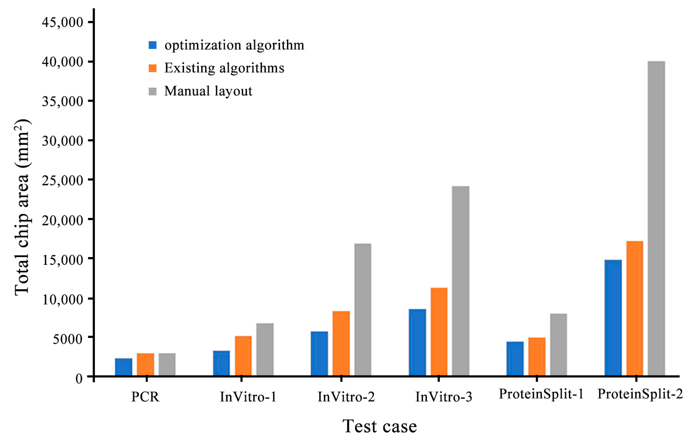
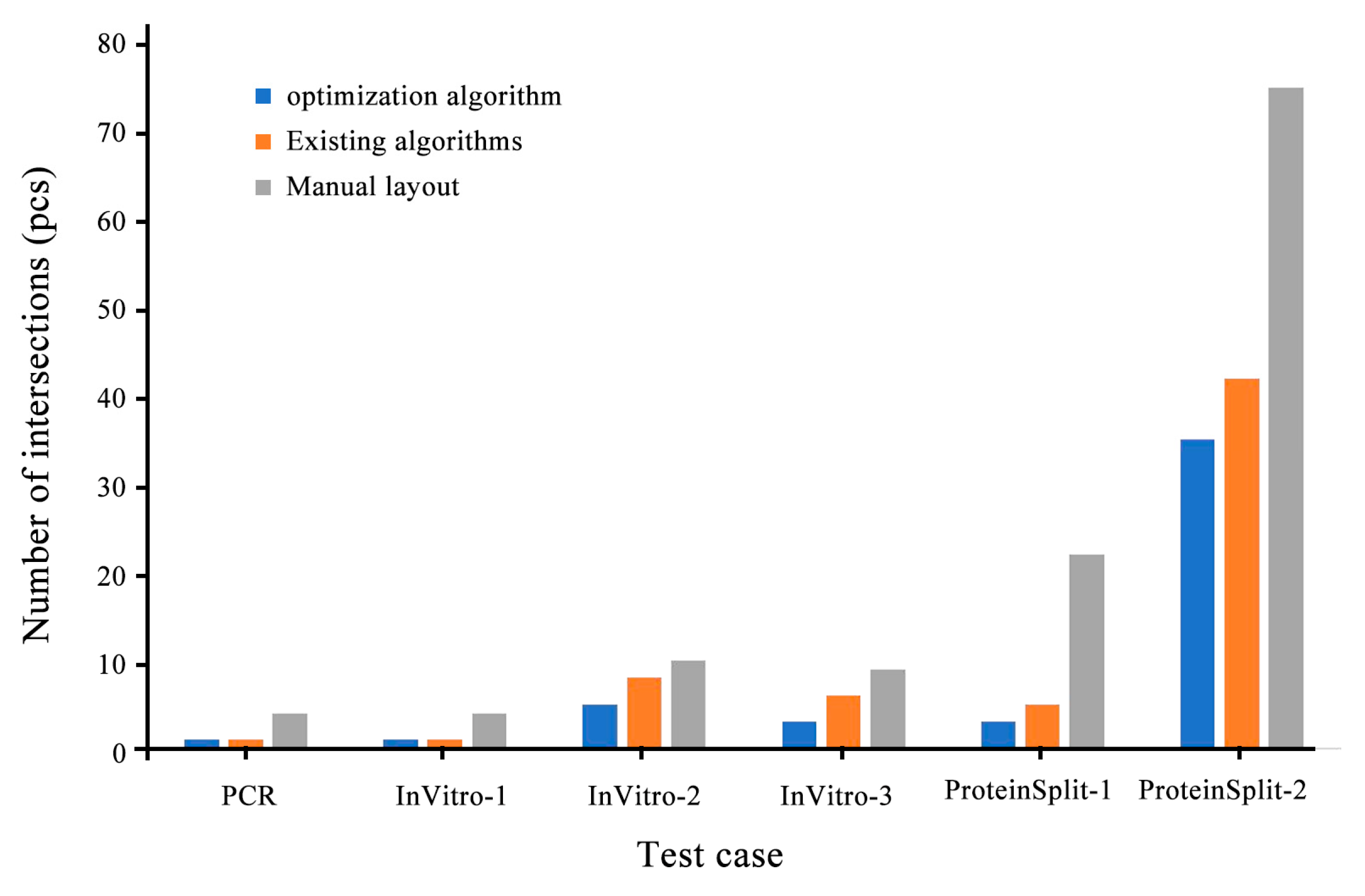
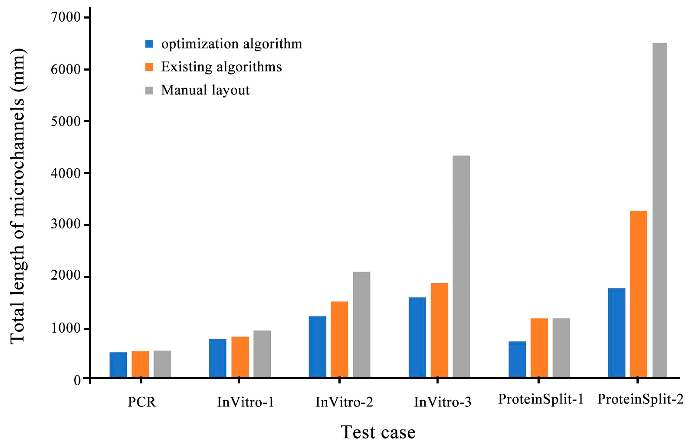
| Test Case | Chip Area (mm2) Existing Algorithm/Optimization Algorithm | Microchannel Length (mm) Existing Algorithm/Optimization Algorithm | Microchannel Intersection (pcs) Existing Algorithm/Optimization Algorithm | CPU Time (s) Existing Algorithm/Optimization Algorithm | Percent Improvement (%) |
|---|---|---|---|---|---|
| PCR | 2958/2850 | 522/509 | 1/1 | 42.7/22.5 | 3.6 |
| InVitro-1 | 5110/3906 | 802/765 | 1/1 | 84.1/63.7 | 23.5 |
| InVitro-2 | 8232/5688 | 1485/1203 | 8/5 | 179.7/170.9 | 30.9 |
| InVitro-3 | 11,187/8460 | 1864/1568 | 6/3 | 301.3/245.6 | 24.3 |
| ProteinSplit-1 | 4914/4422 | 1162/713 | 5/3 | 114.0/106.9 | 10.0 |
| ProteinSplit-2 | 17,030/14,690 | 3247/1749 | 42/35 | 528.0/527.7 | 13.7 |
Disclaimer/Publisher’s Note: The statements, opinions and data contained in all publications are solely those of the individual author(s) and contributor(s) and not of MDPI and/or the editor(s). MDPI and/or the editor(s) disclaim responsibility for any injury to people or property resulting from any ideas, methods, instructions or products referred to in the content. |
© 2023 by the authors. Licensee MDPI, Basel, Switzerland. This article is an open access article distributed under the terms and conditions of the Creative Commons Attribution (CC BY) license (https://creativecommons.org/licenses/by/4.0/).
Share and Cite
Wu, C.; Sun, J.; Almuaalemi, H.Y.M.; Sohan, A.S.M.M.F.; Yin, B. Structural Optimization Design of Microfluidic Chips Based on Fast Sequence Pair Algorithm. Micromachines 2023, 14, 1577. https://doi.org/10.3390/mi14081577
Wu C, Sun J, Almuaalemi HYM, Sohan ASMMF, Yin B. Structural Optimization Design of Microfluidic Chips Based on Fast Sequence Pair Algorithm. Micromachines. 2023; 14(8):1577. https://doi.org/10.3390/mi14081577
Chicago/Turabian StyleWu, Chuang, Jiju Sun, Haithm Yahya Mohammed Almuaalemi, A. S. M. Muhtasim Fuad Sohan, and Binfeng Yin. 2023. "Structural Optimization Design of Microfluidic Chips Based on Fast Sequence Pair Algorithm" Micromachines 14, no. 8: 1577. https://doi.org/10.3390/mi14081577