Article

Efficient Thermal-Stress Coupling Design of Chiplet-Based System with Coaxial TSV Array

1
School of Microelectronics, Xidian University, Xi’an 710071, China
2
CCTEG Ecological Environment Technology Co., Ltd., Beijing 100013, China
*
Authors to whom correspondence should be addressed.
These authors contributed equally to this work.
Micromachines 2023, 14(8), 1493; https://doi.org/10.3390/mi14081493
Submission received: 30 June 2023 / Revised: 19 July 2023 / Accepted: 24 July 2023 / Published: 25 July 2023
(This article belongs to the Special Issue Piezoelectric Materials, Devices and Integrated Systems)

Abstract

:
In this research, an efficient thermal-stress coupling design method for a Chiplet-based system with a coaxial through silicon via (CTSV) array is developed by combining the support vector machine (SVM) model and particle swarm optimization algorithm with linear decreasing inertia weight (PSO-LDIW). The complex and irregular relationship between the structural parameters and critical indexes is analyzed by finite element simulation. According to the simulation data, the SVM model is adopted to characterize the relationship between structural parameters and critical indexes of the CTSV array. Based on the desired critical indexes of the CTSV array, the multi-objective evaluation function is established. Afterwards, the structural parameters of the CTSV array are optimized through the PSO-LDIW algorithm. Finally, the effectiveness of the developed method is verified by the finite element simulation. The simulated peak temperature, peak stress of the Chiplet-based system, and peak stress of the copper column (306.16 K, 28.48 MPa, and 25.76 MPa) well agree with the desired targets (310 K, 30 MPa, and 25 MPa). Therefore, the developed thermal-stress coupling design method can effectively design CTSV arrays for manufacturing high-performance interconnect structures applied in Chiplet-based systems.

1. Introduction

With the development of semiconductor manufacturing processes, Chiplet-based systems have been widely investigated to achieve the continuation of Moore’s law [1,2,3]. Due to the advantages of miniaturization, high performance, and low cost, Chiplet-based systems have been applied in computing systems and processing-in-memory systems [4,5,6]. Through silicon via (TSV) is a key technology to achieve vertical interconnection between different dies in Chiplet-based systems [7,8,9,10,11]. In order to satisfy the requirements of various applications, cylindrical, tapered, and coaxial TSVs (CTSVs) have been proposed [12,13,14]. Due to the advantage of self-shielding, the CTSV can effectively suppress the signal crosstalk and minimize the signal transmission delay, so it has been widely applied in the integrated system [15,16].
The CTSV has been systematically investigated by many researchers in recent years [17,18,19]. Adamshick et al. [20] characterized the thermomechanical behavior of CTSV based on the micro-Raman spectroscopy technique. Yang et al. [21] proposed a new CTSV structure that offers more shielding and less coupling with adjacent structures compared with conventional CTSV. Based on the finite element method (FEM), Qian et al. [22] proposed a distributed transmission line model of silicon-core CTSV. The simulation results observed that the thickness of the plated Cu and isolation dielectric resolved the electrical performance of the silicon-core CTSV. Qiu et al. [23] performed electrical-thermal co-simulation with consideration of the temperature dependence of the metal-oxide-semiconductor effect for CTSV by using equivalent electrical and thermal circuit models. Wang et al. [24] proposed an analytical model for the thermal stress caused by the CTSV and gave guidelines for the design of the CTSV. Dong et al. [25] presented an accurate TSV thermal mechanical stress analytical model, which is verified by FEM. However, the Chiplet-based system with the CTSV array is rarely reported. Therefore, it is valuable to investigate the thermal-stress coupling design of a Chiplet-based system with a CTSV array.
The FEM has the advantages of high computational accuracy, good mesh adaptability, and easy handling of irregular geometric areas, but its disadvantages are that it is time-consuming and inefficient for large-scale simulation [26]. In recent years, data-driven models, such as the support vector machine (SVM) model, neural networks, machine learning, etc., have been applied in medicine, information, industry, etc. Due to their advantages in adaptivity, simplicity, fault tolerance, and robustness, neural networks have been widely used in image processing [27,28], model-predicted control [29,30] data extraction [31,32], etc. The deep neural network has been applied in large-scale integrated systems to describe complex relationships [33]. There are many regression models, such as the linear regression model, the random forest model, the SVM model, etc. Due to its high accuracy, generalization, and non-linear characterization, the SVM model has been used in complex engineering problems such as regression estimation of data, global sensitivity evaluation, and estimation of alloy flow characteristics [34,35,36,37]. The SVM model is good at dealing with linearly indivisible sample data and can effectively avoid data overfitting. In addition, the disadvantages of FEM are that it is time-consuming and inefficient for large-scale simulation, so SVM can be used to replace the FEM model to improve the simulation’s efficiency. At the same time, the particle swarm optimization algorithm with linear decreasing inertia weight (PSO-LDIW) has been widely used in the optimization of electronic components [28,38,39]. Thus, the PSO algorithm can be used to optimize the structural parameters of the CTSV array to design a Chiplet-based system with high thermal stress performance.
In this research, an efficient thermal-stress coupling design method for Chiplet-based systems with CTSV arrays is developed based on the SVM model and PSO-LDIW algorithm. And the highlights can be summarized as follows:
(1)
The complex relationship between structural parameters and critical indexes of the CTSV array is analyzed by FEM simulation.
(2)
The SVM model is established to rapidly characterize the complex relationship between structural parameters and critical indexes of the CTSV array.
(3)
The efficient thermal-stress coupling design method is developed under the framework of the PSO algorithm to control the critical indexes of the CTSV array.
The remainder of this paper is arranged as follows: In Section 2, the modeling and simulation of the thermal-stress coupling CTSV array are presented. In Section 3, the thermal-stress coupling design method for Chiplet-based systems with CTSV arrays is presented. The conclusions are finally given in Section 4.

2. Model and Simulation of Thermal-Stress Coupling CTSV Array

In this research, the FEM model of a Chiplet-based system with a CTSV array is established based on COMSOL software 6.0. In addition, the relationship between structural parameters and critical indexes of the CTSV array is analyzed by the FEM simulation results according to the orthogonal design experiment.

2.1. Thermal-Stress Coupling CTSV Array Model

In this research, a 4 × 4 CTSV array model applied in Chiplet-based systems is established, and the schematic of CTSV in Chiplet-based systems is shown in Figure 1. The CTSV unit is composed of a metal column, a coaxial metal ring, and a dielectric filling layer. The metal column is used to transmit the electrical signal, while the coaxial metal ring is used as a shielding layer for signal interference and noise. The dielectric filling layer is located between the signal layer and the shielding layer. Because of its low resistivity and electrical conductivity [40], copper is commonly used as the TSV-filled material, so the metal column and coaxial metal ring are filled with copper. In addition, the basic properties of the materials used in the FEM model are shown in Table 1. The DC excitation is loaded above the copper column, and the value is 8 × 10¹⁰ A/m2. The electric potential is 0.1 V. The fixed constraint is set around the FEM model. The ambient temperature is 293.15 K. The heat transfer coefficient of convective heat flux is 10 W/(m2·K).

2.2. Simulation and Results

In this research, the structural parameters of the CTSV array are the radius of the copper column (r), the thickness of the dielectric layer (td), the thickness of the coaxial copper ring (rCu), the thickness of the oxide layer between the copper column and shielding layer (t1), the thickness of oxide layer between the coaxial copper ring and shielding layer (t2), the thickness of the oxide layer in the copper ring (t3), the distance between CTSV units (d), and the height of CTSV units (h). The critical indexes of the CTSV array are the peak temperature (PT), peak stress of the Chiplet-based system (PSCS), and copper column (PSCC). The range of r is [1, 3] μm. The ranges of td and rCu are [0.5, 1.5] μm. The ranges of t1, t2, and t3 are [0.05, 0.25] μm. The ranges of d and h are [15, 35] and [40, 80] μm, respectively. The design of the experiment used in this study is an orthogonal experiment. The orthogonal experiment is utilized in the finite element simulation, which includes 8-factors and 9-levels. The orthogonal experiment is shown in Table 2. The number of the FEM simulation is 81, which is obtained by the IBM SPSS Statistics software 24. In the software, the orthogonal plan can be obtained after entering the factors and levels. According to the scheme of orthogonal design, if the level is 9, the number of orthogonal experiments is 81. The simulation results of the CTSV array are shown in Figure 2, based on the orthogonal experiment. These figures are plotted by the Origin 2021 software. According to the orthogonal design, the critical indexes of the CTSV array vary with the structural parameters. The changes in PT with the structural parameters are shown in Figure 2a–d. The range of PT is [300.88, 352.06] K. From Figure 2a, it can be seen that The PT is gradually decreasing with the increase of r. The PT is first increased, then decreased, and finally increased with the increase in td. From Figure 2b,c, the PT is gradually increased and then decreased with the increase of rCu. The PT is gradually increased, then decreased with the increase of t1, t2, and t3. From Figure 2d, the PT first decreases with the increase of d and then gradually increases with the increase in h. The changes in PSCS and PSCC with the structural parameters are shown in Figure 2e–l. The ranges of PSCS and PSCC are [21.05, 176.74] and [13.30, 97.30] MPa, respectively. From Figure 2e,i, it can be seen that the PSCS and PSCC are first increased and then decreased with the increase of r. The PSCS and PSCC are first increased, then decreased, and gradually increased with the increase in td. From Figure 2f,g,j,k, the PSCS and PSCC are increased and then decreased with the increase of rCu. The PSCS and PSCC are gradually increasing with the decrease in t1, t2, and t3. From Figure 2h,l, it can be seen that the PSCS and PSCC are increased with the decrease of d. The PSCS and PSCC decrease with the increase in h. Due to the fact that these eight structural parameters collectively affect the critical index, the above analysis is only a discussion of the approximate variation of the critical indexes with the structural parameters. Undoubtedly, the thermal and stress distributions vary with the structural parameters, and the relationship between the structural parameters and critical indexes of the CTSV array is complex and irregular.

3. Efficient Thermal-Stress Coupling Design for CTSV Array

In this research, an efficient thermal-stress coupling design method for Chiplet-based systems with CTSV arrays is developed by combing the PSO-LDIW algorithm with the SVM model. The flowchart of the developed method is shown in Figure 3, which can be divided into four steps. Firstly, the 4 × 4 CTSV array applied in Chiplet-based systems is established based on COMSOL Multiphysics 6.0. Secondly, the SVM model is established based on the database obtained by orthogonal experiments. Thirdly, the structural parameters of the CTSV array are optimized by the PSO-LDIW algorithm. Finally, the effectiveness of the optimized structural parameters is verified by finite element simulation. The details of the thermal-stress coupling design for the CTSV array are presented as follows:

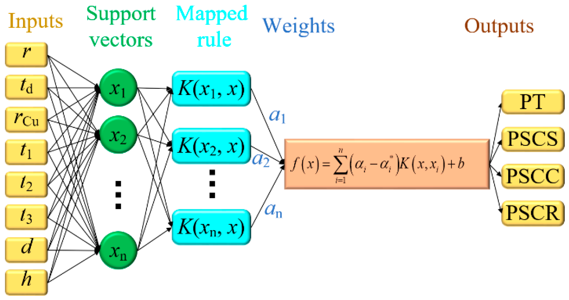
3.1. Critical Database Model and Optimization Algorithm

Based on the simulation results of the orthogonal experiment, the complex relationship between structural parameters and critical indexes of the CTSV array is characterized by the SVM model. The architecture of the SVM model is shown in Figure 4. The capacity constant (C), insensitive parameter (e), and kernel function ( K ( x i , x j ) ) are the key parameters of the SVM model. The inputs of the SVM model are the structural parameters (r, td, rCu, t1, t2, t3, d, h). The outputs are the critical indexes (PT, PSCS, and PSCC). Three multi-input, single-output SVM models are established. The appropriate values of C are 100,000, 100,000, and 100,000. The values of e are 0.1, 1, and 1. The Gauss kernel function is chosen as the kernel function. The validity of the SVM model is tested by taking the data from the FEM simulation results as test samples. The errors of the three SVM models are 3.31 × 10⁻⁷, 3.55 × 10⁻⁶ and 3.02 × 10⁻⁶, respectively, which indicates that the SVM model has high accuracy. When the testing is applied with the data from a training dataset, the error remains at a very low level. The testing data for the established SVM model is shown in Table 3. Obviously, the maximum relative errors for the critical indexes are all less than 5.05%. In the fixed ranges, the higher the accuracy of the established SVM model, the more beneficial the precise design of the CTSV array is.
In addition, the critical indexes of the thermal-stress coupling CTSV array model are the PT, PSCS, and PSCC. The multi-objective evaluation function F has been constructed:
F = α J PT 2 + β J PSCS 2 + γ J PSCC 2
where JPT, JPSCS, and JPSCC represent the optimization criteria for PT, PSCS, and PSCC, respectively. The α, β, and γ are the weight coefficients, and their values are 1/3, respectively. To prevent the influence of magnitude, the optimization criterion after normalization for PT, PSCS, and PSCC can be characterized as
J PT = P T P T des P T max P T min
J PSCS = P S C S P S C S des P S C S max P S C S min
J PSCC = P S C C P S C C des P S C C max P S C C min
where PTdes, PSCSdes, and PSCCdes represent the desired PT, PSCS, and PSCC, respectively. PTmax, PTmin, PSCSmax, PSCSmin, PSCCmax, and PSCCmin are the maximum and minimum of PT, PSCS, and PSCC, respectively. When JPT, JPSCS, and JPSCC are all less than 0 or the algorithm reaches the maximum number of iterations, the optimization algorithm is stopped. The structural parameters of the CTSV array are optimized by the PSO-LDIW algorithm, and the pseudocode is presented in Algorithm 1. The parameters used in the PSO-LDIW algorithm are shown in Table 4. The desired target values of PT, PSCS, and PSCC are determined based on extensive simulation analysis. These desired target values are as small as possible. In addition, the multi-objective evaluation function is established based on the desired target values. And then, the PSO-LDIW algorithm is used to optimize the structural parameters of the CTSV array so that the critical indexes can reach the desired target values as close as possible.
Algorithm 1 Pseudocode of the efficient thermal-stress coupling design of CTSV array under the framework of PSO algorithm
1Initialize population
2for t = 1:maximum generation
3  Initialize local and global best particles (pi and pg)
4  for i = 1:population size
5   for d = 1:dimension
6    vi,d(t + 1) = w(t)vi,d(t) + c1r1(pi-xi,d(t)) + c2r2(pg-xi,d(t));
7      if vi,d(t + 1) > vmax then vi,d(t + 1) = vmax;
8          else if vi,d(t + 1) < vmin then vi,d(t + 1) = vmin;
9      end
10        xi,d(t + 1) = xi,d(t) + vi,d(t+1);
11        if xi,d(t + 1) > xmax then xi,d(t + 1) = xmax;
12          else if xi,d(t + 1) < xmin then xi,d(t + 1) = xmin;
13        end
14     end
15     if f(xi,d(t)) < f(pi(t)) then pi(t) = xi,d(t);
16     end
17  end
18  f(pg(t)) < mini(f(pi(t)));
19  w(t) = [(tmaxt)/tmax](wmaxwmin) + wmin
20  Pbest(t) = f(pg(t))
21  if Pbest(t) < eps then break;
22  end
23End
xi and vi represent the position and velocity of the ith particle; pi is the best previous position of the ith particle, and pg is the best previous position of all particles; tmax is the maximum number of iterations; w, wmax, and wmin are the inertia weight, upper and lower bounds of inertia weight, respectively.

3.2. Verification and Discussion

In this research, the efficient thermal-stress coupling design method of CTSV arrays is applied to optimize the structural parameters of CTSV arrays. According to the optimization algorithm, the optimized r, td, rCu, t1, t2, t3, d, and h are 1, 1.25, 0.64, 0.22, 0.08, 0.15, 28.19, and 53.92 μm, respectively. The simulation results of the FEM model at the optimized structural parameters are shown in Figure 5. The contour surfaces of temperature and stress of the verified results are shown in Figure 6. Clearly, the temperature is higher in the center of the CTSV unit, and the stress distribution is distorted at the interface of different materials. The verified PT, PSCS, and PSCC are 306.16 K, 28.48 MPa, and 25.76 MPa, respectively, while the desired targets are 310 K, 30 MPa, and 25 MPa. Obviously, the verified results agree well with the desired targets. This is because the established SVM model can accurately characterize the FEM model of the CTSV array applied in a Chiplet-based system.
In addition, two 2D cross-sections are established to analyze the thermal and stress distribution of the CTSV array. The simulation results are shown in Figure 7. From Figure 7a, the cross-section is x = 28.297 μm. Obviously, the temperature is higher in the center, and the trend of temperature is decreasing from the center to the marginal region. From Figure 7b,c, the cross-section is z = 26.96 μm. The peak stress is located at the interface between different materials. This is because a mismatch in the coefficient of thermal expansion exists between different materials. Moreover, three lines are established to analyze the critical index distribution on the cross section. The simulation results are shown in Figure 8. The temperature curves of the horizontal line (from point (28.297, −14.095, 26.96) to point (28.297, 98.665, 26.96)) are presented in Figure 8a. Clearly, the temperature gradually increases from the edge to the center of the copper column. The stress curves of the horizontal line (from point (0, −14.095, 26.96) to point (0, 98.665, 26.96)) and vertical line (from point (−0.233, −0.287, 0) to point (−0.233, −0.287, 53.92)) are presented in Figure 8b,c. Due to the mismatch of coefficients of thermal expansion between different materials, the stress distribution is buried at the interface of different materials, and the PSCC is located at approximately h/2.
The critical indexes of desired, predicted, and verified CTSV arrays are presented in Table 5. The relative errors between the verified and desired targets are all less than 5.07%, while the relative errors between the predicted and desired targets are all less than 2.08%. Clearly, the error exists in the established SVM model, and the computation accuracy of the FEM model is higher than that of the SVM model. In addition, the verified results (306.16 K, 28.48 MPa, and 25.76 MPa) well agree with the desired targets (310 K, 30 MPa, and 25 MPa). Thus, a CTSV array with controllable thermal stress distribution can be obtained by the developed method.
In this research, the CPU of the workstation is Intel(R) Xeon(R) Gold 6242R. The average run time of the SVM model based on MATLAB R2022b is less than 0.05 s, while the average run time of the finite element model based on COMSOL Multiphysics 6.0 is 404 s. Evidently, the FEM simulation is time-consuming and inefficient. In order to increase the simulation efficiency, the SVM is established to characterize the FEM model. In addition, the PSO-LDIW algorithm is adopted to obtain the optimal structural parameters to control the critical indexes of the CTSV array. The average run time of the thermal-stress coupling design based on the SVM model and PSO-LDIW algorithm for one independent run is less than 210 s, while the design cycle of the traditional FEM method is several days to a month for different designers. Thus, the design efficiency of the developed method for CTSV arrays is greatly increased compared with the traditional method. In the future, the placement and routing of Chiplet-based systems with CTSV arrays will be investigated. The range of structural parameters will be expanded to investigate the error of the SVM model, and the dataset will be divided into the training dataset and the testing dataset. The application of the thermal-stress coupling design to more types of TSV structures and more complex 3D integrated circuits with multi-layer structures will also be investigated.

4. Conclusions

In this research, an efficient thermal-stress coupling design method for Chiplet-based systems with CTSV arrays is developed based on the SVM model and PSO-LDIW algorithm, which can control the critical indexes of CTSV arrays. The conclusions are summarized as follows:
(1)
The relationship between structural parameters and critical indexes of the CTSV array is analyzed based on the established CTSV array model, and it is irregular and complex;
(2)
The SVM model is utilized to characterize the complex and irregular relationship between structural parameters and critical indexes of the CTSV array, and the average run time of the SVM model is less than 0.05 s;
(3)
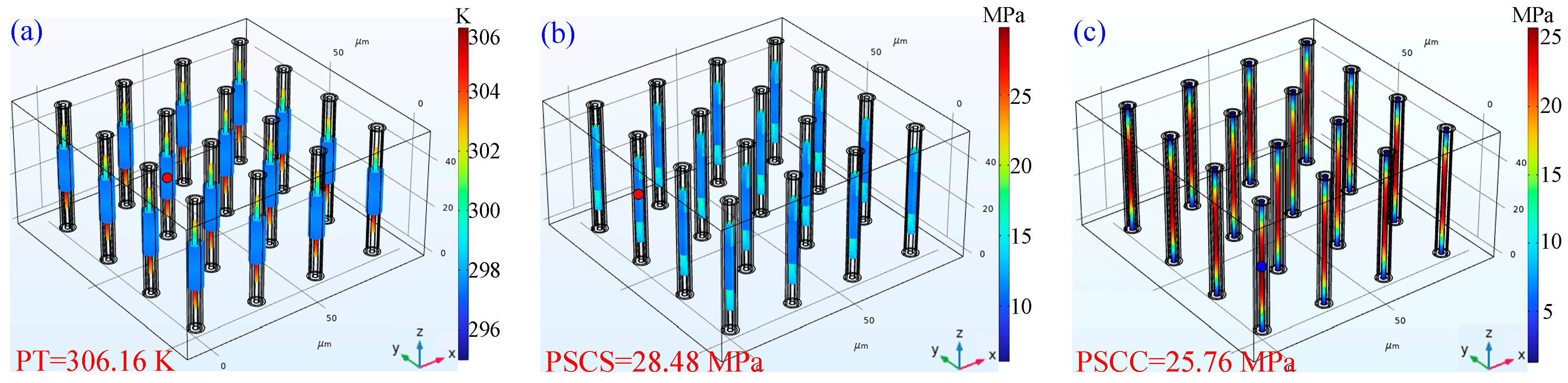
The critical indexes of the CTSV array applied in Chiplet-based systems can be controlled by the developed method. The verified results (306.16 K, 28.48 MPa, and 25.76 MPa) well agree with the desired targets (310 K, 30 MPa, and 25 MPa). The average run time of the method for one independent run is less than 210 s, which is much less than the conventional method.

Author Contributions

Conceptualization, X.W., J.S. and D.C.; resources, X.W. and J.S.; writing-original draft preparation, X.W. and J.S.; data curation, D.L.; writing-reviewing and editing, D.C. and D.L.; supervision, G.L. and Y.Y. All authors have read and agreed to the published version of the manuscript.

Funding

This work was supported in part by the Fundamental Research Funds for the Central Universities under Grant QTZX23022, in part by the Innovation Fund of Xidian University under Grant YJSJ23019, in part by the Youth Talent Fund of the Joint Fund of The Ministry of Education for Equipment Pre-Research under Grant 8091B032138, in part by the National Natural Science Foundations of China under Grant 62104177, in part by the Cooperation Program of XDU-Chongqing IC Innovation Research Institute under Grant CQIRI-2022CXY-Z01, and in part by the Equipment Pre-Research Project of China under Grant 80924020307.

Data Availability Statement

Not applicable.

Conflicts of Interest

The authors declare no conflict of interest.

References

  1. Moore, S.K. Chiplets are the future of processors: Three advances boost performance, cut costs, and save power. IEEE Spectr. 2020, 57, 11–12. [Google Scholar] [CrossRef]
  2. Croes, K.; De Messemaeker, J.; Li, Y.; Guo, W.; Pedreira, O.V.; Cherman, V.; Stucchi, M.; De Wolf, I.; Beyne, E. Reliability Challenges Related to TSV Integration and 3-D Stacking. IEEE Des. Test 2016, 33, 37–45. [Google Scholar] [CrossRef]
  3. Coudrain, P.; Souare, P.M.; Prieto, R.; Fiori, V.; Farcy, A.; Pailleur, L.L.; Colonna, J.-P.; Santos, C.; Vivet, P.; Ben-Jamaa, H.; et al. Experimental Insights Into Thermal Dissipation in TSV-Based 3-D Integrated Circuits. IEEE Des. Test 2016, 33, 21–36. [Google Scholar] [CrossRef]
  4. Shan, G.; Zheng, Y.; Xing, C.; Chen, D.; Li, G.; Yang, Y. Architecture of Computing System based on Chiplet. Micromachines 2022, 13, 205. [Google Scholar] [CrossRef] [PubMed]
  5. Li, T.; Hou, J.; Yan, J.; Liu, R.; Yang, H.; Sun, Z. Chiplet Heterogeneous Integration Technology—Status and Challenges. Electronics 2020, 9, 670. [Google Scholar] [CrossRef] [Green Version]
  6. Ma, X.; Wang, Y.; Wang, Y.; Cai, X.; Han, Y. Survey on Chiplets: Interface, interconnect and integration methodology. CCF Trans. HPC 2022, 4, 43–52. [Google Scholar] [CrossRef]
  7. Cong, J.; Luo, G.; Wei, J.; Zhang, Y. Thermal-Aware 3D IC Placement Via Transformation. In Proceedings of the 2007 Asia and South Pacific Design Automation Conference, Yokohama, Japan, 23–26 January 2007; pp. 780–785. [Google Scholar]
  8. Thadesar, P.A.; Gu, X.; Alapati, R.; Bakir, M.S. Through-Silicon Vias: Drivers, Performance, and Innovations. IEEE Trans. Compon. Packag. Manuf. Technol. 2016, 6, 1007–1017. [Google Scholar] [CrossRef]
  9. Zhou, M.; Li, L.; Hou, F.; He, G.; Fan, J. Thermal Modeling of a Chiplet-Based Packaging with a 2.5-D Through-Silicon Via Interposer. IEEE Trans. Compon. Packag. Manuf. Technol. 2022, 12, 956–963. [Google Scholar] [CrossRef]
  10. Lau, J.H. Recent Advances and Trends in Multiple System and Heterogeneous Integration with TSV Interposers. IEEE Trans. Compon. Packag. Manuf. Technol. 2023, 13, 3–25. [Google Scholar] [CrossRef]
  11. Rao, X.; Song, J.; Tian, Q.; Liu, H.; Jin, C.; Xiao, C. A universal and efficient equivalent modeling method for thermal analysis of 3D ICs containing tapered TSVs. Int. Commun. Heat Mass Transf. 2022, 136, 106161. [Google Scholar] [CrossRef]
  12. Xu, Z.; Lu, J.-Q. Three-Dimensional Coaxial Through-Silicon-Via (TSV) Design. IEEE Electron. Device Lett. 2012, 33, 1441–1443. [Google Scholar] [CrossRef]
  13. Qian, L.; Qian, K.; He, X.; Chu, Z.; Ye, Y.; Shi, G.; Xia, Y. Through-Silicon Via-Based Capacitor and Its Application in LDO Regulator Design. IEEE Trans. VLSI Syst. 2019, 27, 1947–1951. [Google Scholar] [CrossRef]
  14. Lu, T.; Serafy, C.; Yang, Z.; Samal, S.K.; Lim, S.K.; Srivastava, A. TSV-Based 3-D ICs: Design Methods and Tools. IEEE Trans. Comput. Aid Des. 2017, 36, 1593–1619. [Google Scholar] [CrossRef]
  15. Xu, Z.; Lu, J.-Q. Through-Silicon-Via Fabrication Technologies, Passives Extraction, and Electrical Modeling for 3-D Integration/Packaging. IEEE Trans. Semicond. Manuf. 2013, 26, 23–34. [Google Scholar] [CrossRef]
  16. Mei, Z.; Dong, G. A Simplified Closed-Form Model and Analysis for Coaxial-Annular Through-Silicon Via in 3-D ICs. IEEE Trans. Compon. Packag. Manuf. Technol. 2018, 8, 1650–1657. [Google Scholar] [CrossRef]
  17. Zhao, W.-S.; Zheng, J.; Wang, J.; Liang, F.; Wen, F.; Dong, L.; Wang, D.; Wang, G. Modeling and Characterization of Coaxial Through-Silicon via with Electrically Floating Inner Silicon. IEEE Trans. Compon. Packag. Manuf. Technol. 2017, 7, 936–943. [Google Scholar] [CrossRef]
  18. Su, J.; Zhang, W.; Yao, C. Partial Coaxial Through-Silicon via for Suppressing the Substrate Noise in 3-Dimensional Integrated Circuit. IEEE Access 2019, 7, 98803–98810. [Google Scholar] [CrossRef]
  19. Chen, D.; Yang, Y.; Wang, X.; Li, D.; Liang, Y.; Xu, C. Thermal-Stress Coupling Optimization for Coaxial through Silicon Via. Symmetry 2023, 15, 264. [Google Scholar] [CrossRef]
  20. Adamshick, S.; Northrup, S.; Liehr, M. Experimental characterization of coaxial TSV transistor keep out zones. Micro Nano Lett. 2018, 13, 1457–1459. [Google Scholar] [CrossRef]
  21. Yang, Y.; Zheng, J.; Dong, G.; Zhao, Y.; Mei, Z.; Zhu, W. New coaxial through silicon via (TSV) applied for three dimensional integrated circuits (3D ICs). IEICE Electron. Expr. 2016, 13, 20160192. [Google Scholar] [CrossRef] [Green Version]
  22. Qian, L.; Xia, Y.; He, X.; Qian, K.; Wang, J. Electrical Modeling and Characterization of Silicon-Core Coaxial Through-Silicon Vias in 3-D Integration. IEEE Trans. Compon. Packag. Manuf. Technol. 2018, 8, 1336–1343. [Google Scholar] [CrossRef]
  23. Min, Q.; Li, E.-P.; Jin, J.-M.; Chen, W. Electrical–Thermal Cosimulation of Coaxial TSVs with Temperature-Dependent MOS Effect Using Equivalent Circuit Models. IEEE Trans Electromagn. Compat. 2020, 62, 2247–2256. [Google Scholar] [CrossRef]
  24. Wang, F.; Zhu, Z.; Yang, Y.; Liu, X.; Ding, R. Thermo-mechanical performance of Cu and SiO2 filled coaxial through-silicon-via (TSV). IEICE Electron. Expr. 2013, 10, 20130894. [Google Scholar] [CrossRef] [Green Version]
  25. Dong, G.; Shi, T.; Zhao, Y.; Yang, Y. An analytical model of thermal mechanical stress induced by through silicon via. Chin. Phys. B 2015, 24, 056601. [Google Scholar] [CrossRef]
  26. Kolbehdari, M.A.; Srinivasan, M.; Nakhla, M.S.; Zhang, Q.-J.; Achar, R. Simultaneous time and frequency domain solutions of EM problems using finite element and CFH techniques. IEEE Trans. Microw. Theory Tech. 1996, 44, 1526–1534. [Google Scholar] [CrossRef]
  27. Abuzneid, M.A.; Mahmood, A. Enhanced Human Face Recognition Using LBPH Descriptor, Multi-KNN, and Back-Propagation Neural Network. IEEE Access 2018, 6, 20641–20651. [Google Scholar] [CrossRef]
  28. Xu, L.; Zhang, Z.; Yao, Y.; Yu, Z. Improved Particle Swarm Optimization-Based BP Neural Networks for Aero-Optical Imaging Deviation Prediction. IEEE Access 2022, 10, 26769–26777. [Google Scholar] [CrossRef]
  29. Lin, Y.C.; Chen, D.D.; Chen, M.S.; Chen, X.M.; Li, J. A precise BP neural network-based online model predictive control strategy for die forging hydraulic press machine. Neural. Comput. Appl. 2018, 9, 585–596. [Google Scholar] [CrossRef]
  30. Chen, D.D.; Lin, Y.C.; Wu, F. A design framework for optimizing forming processing parameters based on matrix cellular automaton and neural network-based model predictive control methods. Appl. Math. Model. 2019, 76, 918–937. [Google Scholar] [CrossRef]
  31. Wang, W.; Liu, W.; Chen, H. Information Granules-Based BP Neural Network for Long-Term Prediction of Time Series. IEEE Trans. Fuzzy Syst. 2021, 29, 2975–2987. [Google Scholar] [CrossRef]
  32. Han, M.; Cheng, L.; Meng, H. Application of four-layer neural network on information extraction. Neural Netw. 2003, 16, 547–553. [Google Scholar] [CrossRef]
  33. Pandey, S.; Panda, P.R. NeuroMap: Efficient Task Mapping of Deep Neural Networks for Dynamic Thermal Management in High-Bandwidth Memory. IEEE Trans. Comput.-Aided Des. Integr. Circuits Syst. 2022, 41, 3602–3613. [Google Scholar] [CrossRef]
  34. Grinblat, G.L.; Uzal, L.C.; Verdes, P.F.; Granitto, P.M. Nonstationary regression with support vector machines. Neural. Comput. Appl. 2015, 26, 641–649. [Google Scholar] [CrossRef]
  35. Ruan, Y.; Zou, Y.; Chen, M.; Shen, J. Monitoring the Spatiotemporal Trajectory of Urban Area Hotspots Using the SVM Regression Method Based on NPP-VIIRS Imagery. ISPRS Int. J. Geoinf. 2021, 10, 415. [Google Scholar] [CrossRef]
  36. He, D.; Lin, Y.; Chen, J.; Chen, D.; Huang, J.; Tian, Y.; Chen, M. Microstructural evolution and support vector regression model for an aged Ni-based superalloy during two-stage hot forming with stepped strain rates. Mater. Des. 2018, 154, 51–62. [Google Scholar] [CrossRef]
  37. Wang, L.; Li, L.; Zhang, Z. Accurate Descriptions of Hot Flow Behaviors across β Transus of Ti-6Al-4V Alloy by Intelligence Algorithm GA-SVR. J. Mater. Eng. Perform. 2016, 25, 3912–3923. [Google Scholar] [CrossRef]
  38. Chen, D.; Zhao, J.; Fei, C.; Li, D.; Zhu, Y.; Li, Z.; Guo, R.; Lou, L.; Feng, W.; Yang, Y. Particle Swarm Optimization Algorithm-Based Design Method for Ultrasonic Transducers. Micromachines 2020, 11, 715. [Google Scholar] [CrossRef] [PubMed]
  39. Chen, D.; Lin, Y. A particle swarm optimization-based multi-level processing parameters optimization method for controlling microstructures of an aged superalloy during isothermal forging. Met. Mater. Int. 2019, 25, 1246–1257. [Google Scholar] [CrossRef]
  40. Liu, X.; Thadesar, P.A.; Taylor, C.L.; Oh, H.; Kunz, M.; Tamura, N.; Bakir, M.S.; Sitaraman, S.K. Insitu microscale through-silicon via strain measurements by synchrotron X-ray microdiffraction exploring the physics behind data interpretation. Appl. Phys. Lett. 2014, 105, 112109. [Google Scholar] [CrossRef] [Green Version]
Figure 1. Schematic of CTSV in Chiplet-based system.
Micromachines 14 01493 g001
Figure 2. Simulation results based on the orthogonal experiments: (ad): peak temperature; (eh): peak stress of the Chiplet-based system; (il): peak stress of copper column.
Micromachines 14 01493 g002
Figure 3. Flowchart of the developed method.
Micromachines 14 01493 g003
Figure 4. Architecture of support vector machine model.
Micromachines 14 01493 g004
Figure 5. Verified results of FEM model at the optimized parameters: (a) PT; (b) PSCS; (c) PSCC.
Micromachines 14 01493 g005
Figure 6. Contour surface of temperature and stress of the verified results: (a) temperature; (b) stress.
Micromachines 14 01493 g006
Figure 7. Verified results on the cross section: (a) PT; (b) PSCS; (c) PSCC.
Micromachines 14 01493 g007
Figure 8. Indexes distribution on the cross section: (a) Temperature distribution; (b) Stress distribution; (c) Stress distribution of copper column (SCC).
Micromachines 14 01493 g008
Table 1. Physical parameters of material used in the FEM model.
PropertyCopperSiSiO2
Relative permittivity111.74.2
Heat capacity at constant pressure (J/(kg·K))385700730
Coefficient of thermal expansion (1/K) × 106172.60.5
Density (kg/m3)896023292200
Thermal conductivity (W/(m·K))4001301.4
Young’s modulus (GPa)17017070
Poisson’s ratio0.280.280.17
Table 2. Orthogonal experiment.
Factors123456789
r11.21.51.822.22.52.83
td0.50.60.70.811.11.31.41.5
rCu0.50.60.70.811.11.31.41.5
t10.050.080.10.130.150.180.20.220.25
t20.050.080.10.130.150.180.20.220.25
t30.050.080.10.130.150.180.20.220.25
d151720222528303335
h404550556065707580
Table 3. Testing data for the established SVM model.
rtdrCut1t2t3dhFEMSVMMaximum Relative Error %
PT (K)PSCS (MPa)PSCC (MPa)PT (K)PSCS (MPa)PSCC (MPa)
20.81.10.10.150.153560319.5571.3645.54322.0968.7143.355.05
21.31.10.10.150.153060316.8764.4440.57322.164.7340.471.62
20.81.10.10.150.153560318.769.0143.99322.0968.7143.351.05
1.811.10.150.130.153060317.561.8843.47322.160.841.524.69
1.811.10.130.150.183565318.1864.6844.80322.0966.9544.441.21
1.811.10.130.150.153060317.1162.1042.5532261.640.84.29
Table 4. Parameters of the efficient thermal-stress coupling design of CTSV array.
Parameters of Optimization CriteriaDesired Critical IndexesPTdes = 310 K, PSCSdes = 30 MPa, PSCCdes = 25 MPa
Parameters of PSO-LDIW algorithmConstant parametersc1 = c2 = 2
Range of inertia weight w 0.4 , 0.9
Maximum generationtmax = 100
Dimension of search spaceD = 8
Population sizeN = 400
Range of particle position x r 1 , 3 , x t 1 , t 2 . t 3 0.05 , 0.25 , x t d , r Cu 0.5 , 1.5 x d 15 , 35 , x h 40 , 80
Range of particle velocity v r 1 , 1 , v t 1 , t 2 , t 3 0.1 , 0.1 , v t d , r Cu 0.5 , 0.5 v d 1 , 1 , v h 5 , 5
Table 5. Critical indexes of CTSV array at the optimized parameters.
IndexesPT (K)PSCS (MPa)PSCC (MPa)
Desired3103025
Predicted31029.5225.52
Verified306.1628.4825.76
Disclaimer/Publisher’s Note: The statements, opinions and data contained in all publications are solely those of the individual author(s) and contributor(s) and not of MDPI and/or the editor(s). MDPI and/or the editor(s) disclaim responsibility for any injury to people or property resulting from any ideas, methods, instructions or products referred to in the content.

