1. Introduction
Street lighting is important equipment for sidewalks and roadways, and can impact traffic safety and the quality of the human environment to serve a sense of conformability and security. Moreover, street lighting can also improve the daytime and night appearance of the road environment. To ensure a good installation, street lighting standards require several performance indexes, such as illuminance, luminance, power qualities, and electrical conversion efficiencies [
1,
2,
3].
The light-emitting diode (LED) can be used in indoor and outdoor environments including roadways, sidewalks, streets, building interiors, advertisement signboards, and ambient lighting. In street lighting applications, LEDs have more lifetime (50–100 k hours) compared with that of fluorescent or gas-discharge lamps, substantially reducing maintenance and replacement costs [
4].
General LED drivers are composed of a power factor correction (PFC) circuit, DC–DC converter, and current control circuit. To promote the conversion efficiency and hardware reliability of the LED driver, the single-stage AC–DC converter as an alternative to the PFC circuit and the DC-DC converter has been developed and implemented [
5].
Due to the greenhouse effect and climate change influences, science and technology development is placing more and more focus to energy saving and carbon reduction. Therefore, switching-mode power supplies (SMPSs) play a critical role in power conversion. SMPSs have isolated and non-isolated topologies. Non-isolated SMPSs include buck converters, boost converters, and boost-buck converters. Isolated SMPSs include full-bridge converters, half-bridge converters, forward converters, and flyback converters.
An isolated power converter separates the input alternating-current (AC) power from the output direct-current (DC) power by electrically and physically dividing the circuit into two sections, in order to prevent the AC power from influencing the load. The isolated AC–DC converter uses a high-frequency transformer to achieve galvanic isolation between the AC inlet and DC outlet.
Several benefits of isolated AC–DC converters include:
Therefore, isolated AC–DC converters have been used in medical, industrial, instrumentation, smart home, commercial electronic equipment, internet of things (IoT), telecommunication, battery charger, cell phone charger, vehicle or aircraft powertrains, military, and home applications [
6].
Comparing the forward converter and the flyback converter, the transformer of the flyback converter dispenses with an additional demagnetization winding, hence the design difficulty and transformer winding cost can be reduced. Moreover, a quasi-resonant (QR)-flyback converter can achieve soft-switching for the power switch using the transformer’s primary inductance and the switch’s and circuit board’s parasitic capacitances; therefore, the conducted and radiated electromagnetic interferences can be reduced [
7,
8]. Otherwise, in order to improve the power conversion efficiency, retain the advantages of simple circuit configuration, and reduce the hardware cost, QR-flyback converters have become popular.
QR-flyback converters use the parasitic capacitance on the power switch and leakage inductance on the transformer to generate a resonant voltage when the power switch is turned off, and then the power switch can be turned on at the resonant voltage valley; therefore, soft-switching can be achieved to reduce switching losses, and electromagnetic interference can be effectively diminished. Moreover, the QR-flyback converter is an isolated SMPS because it possesses a transformer; furthermore, the QR-flyback converter can use a pulse-width modulation (PWM) control chip to correct the power factor of the input AC power; in summary, the QR-flyback converter is suitable as a driving power supply for LED array streetlamps [
9,
10].
Table 1 lists the characteristic differences between a hard-switching traditional flyback and soft-switching QR-flyback [
7,
8,
11].
This study developed and implemented a QR-flyback converter driving an LED array streetlamp. Using a PWM control IC, the QR-flyback converter can achieve the power factor correction and drive the LED array streetlamp; moreover, the bright and extinguishable control circuit incorporating the PWM control IC could control the LED array streetlamp’s brightness and extinguishing operations.
2. Design Consideration of QR-Flyback Converter
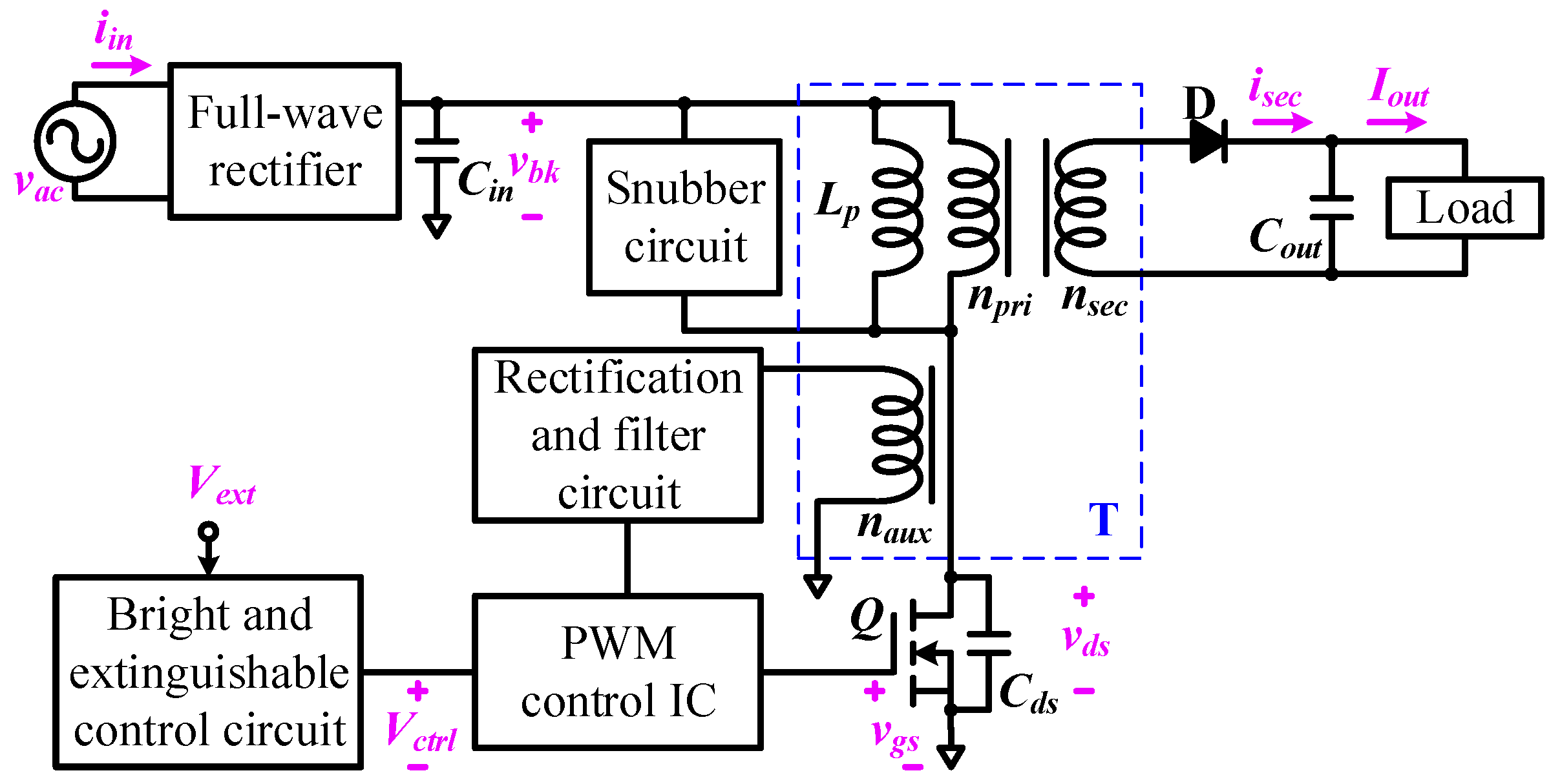
The circuit block diagram of the QR-flyback converter is depicted in
Figure 1, including the full-wave rectifier, input filter capacitor
Cin, snubber circuit, rectification and filter circuit, PWM control chip,
n-channel metal-oxide-semiconductor field-effect transistor (MOSFET) switch Q, drain-source terminal capacitor
Cds, bright and extinguishable control circuit, transformer T (including the magnetizing inductance
Lp, primary-side winding
npri, secondary-side winding
nsec, and auxiliary winding
naux), diode D, and output filter capacitor
Cout; the input source is the AC voltage
vac, and the output power drives the load. The QR-flyback converter specification, transformer design, MOSFET switch specification, snubber design, secondary-side rectifier diode design, and input and output filter capacitor designs are described as follows:
2.1. QR-Flyback Converter Specification
The specifications of the developed QR-flyback converter are listed in
Table 2.
2.2. Transformer Design
The terminal voltage across the transformer’s secondary side can be reflected to the transformer’s primary side, becoming a reflected voltage
VR. The minimum peak value of the input AC voltage is
vac(pk,min); a variable
kv can be obtained and expressed as [
12]:
Substitution of
VR = 100 V and
vac(pk,min) = 85
= 120 V into (1) can obtain
kv = 1.2. Using the characteristic equation:
f(
kv) = (0.5 +
kv × 1.4 × 10
−3)/(1 + 0.82 ×
kv) [
12],
f(
kv) = 0.25 can be obtained.
N27 and EF25 are the model numbers of the magnetic core material and transformer bobbin in the study application. The effective magnetic path length
le = 57.5 mm, effective magnetic cross-sectional area
Ae = 52.5 mm
2, and effective volume
Ve = 3020 mm
3 [
13]. To ensure that the designed transformer is not operated in saturation, it is necessary to calculate the minimum magnetizing inductance
Lp(min) in the primary-side winding of the transformer.
Lp(min) can be expressed as [
12]:
where
ip(pk) is the peak current passing the magnetizing inductance, which can be expressed as [
12]:
where
Pin(max) is the maximum input power. In
Table 1, the output power of the QR-flyback converter is
Pout = 52.5 W, and the conversion efficiency is set at 80%, hence
Pin(max) can be calculated as 65.63 W; in this study,
Pin(max) = 70 W was used. Substitution of
Pin(max) = 70 W,
vac(pk,min) = 120 V, and
f(
kv) = 0.25 into (3) can yield
ip(pk) = 4.7 A. Substitution of the aforementioned parameters and
VR = 100 V into (2) can obtain
Lp(min) = 99 μH. According to [
14], another magnetizing inductance equation can be expressed as:
where
fsw(min) is the minimum operating frequency of the MOSFET switch, and its value is
fsw(min) = 80 kHz. Substitution of
vac(pk,min) = 120 V,
kv = 1.2,
fsw(min) = 80 kHz, and
ip(pk) = 4.7 A into (4) can yield
Lp = 145.07 μH, which is greater than
Lp(min) = 99 μH.
The calculating expression of
npri can be expressed as [
12,
14]:
Substitution of Lp = 145.07 μH, ip(pk) = 4.7 A, Bmax = 0.3 mT, and Ae = 52.5 mm2 into (5) can obtain npri = 43.29 ≅ 44, because the winding turns in practical applications are the positive integer.
The turn ratio
n of transformer can be expressed as [
12]:
where
Vf is the forward bias voltage of D. Substitution of
Vf = 0.8 V,
VR = 100 V, and
Vout = 35 V into (6) can obtain
nsec = 15.75 ≅ 16. Using both
npri = 44 and
nsec = 16,
n = 2.75 can be obtained.
The calculating expression of
naux can be expressed as [
12]:
where
Vaux is a voltage across the auxiliary winding; in this study, the operating power of the PWM control chip was set to 15 V. Substitution of
Vaux = 15 V,
Vout = 35 V, and
nsec = 16 into (7) can obtain
naux = 6.86 ≅ 7. Aforementioned parameters include
n = 2.75,
npri = 44,
nsec = 16,
naux = 7, and
Lp = 145.07 μH.
2.3. Metal-Oxide-Semiconductor Field-Effect Transistor (MOSFET) Specification
The withstand voltage and current are the important specifications for MOSFET switch selection. When the MOSFET switch is turned off, the leakage inductance on the transformer and paratactic capacitance on the MOSFET switch cause the resonant voltage spike
vspike, hence the withstand voltage of the MOSFET switch must be greater than
vspike, which can be expressed as [
15]:
where
Lleak is the leakage inductance on the primary side of the transformer. It is usually 1% to 3% of
Lp, hence
Lleak =
Lp × 1% = 145.07 μH × 1% = 1.45 μH in this study. Moreover,
Cds is the drain-source terminal capacitance on the MOSFET switch, and the
Cds = 470 pF was used in this study. Substitution of
ip(pk) = 4.7 A,
Lleak = 1.45 μH, and
Cds = 470 pF into (8) can obtain
vspike = 261.06 V. The withstand voltage of the MOSFET switch can be expressed as [
12]:
Substitution of
vac(pk,max) = 198 V,
VR = 100 V, and
vspike = 261.06 V into (9) can obtain
Vbreak = 559.06 V, hence the withstand voltage of the MOSFET switch must be greater than 559.06 V. Moreover, the withstand current of the MOSFET switch must be greater than
ip(pk) = 4.7 A. Furthermore, the small
Cds and gate terminal charge
Qg can be selected for switching loss reduction. The model number STF10N80K5 of the MOSFET switch [
16] was used in this study, its specifications listed in
Table 3.
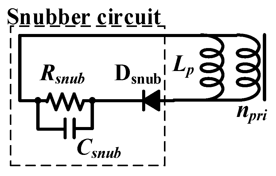
2.4. Snubber Circuit
The resonant voltage spike generated by the QR-flyback converter exceeds the withstand voltage of the MOSFET switch, resulting in device damage. The voltage spike can be reduced by the snubber circuit. The snubber circuit elements include a resistor
Rsnub,
Csnub, and
Dsnu, as shown in
Figure 2.
Rsnub and
Csnub can be expressed as [
17]:
Substitution of Lleak = 1.45 μH, ip(pk) = 4.7 A, vspike = 261.06 V, and VR = 100 V into (10) can obtain Csnub = 266.11 pF. Substitution of the aforementioned parameters and fsw(min) = 80 kHz into (11) can yield Rsnub = 36.59 kΩ. The diode Dsnu of the snubber circuit can use a fast recovery diode, whose recovery time can reduce the switching loss of Dsnu.
2.5. Rectification Diode
The withstand voltage calculation of the rectification diode D can be expressed as [
12]:
Substitution of Vout = 35 V, vac(pk,max) = 198 V, npri = 44, and nsec = 16 into (12) can obtain Vd = 107 V.
According to the transformer reflection law, the peak current calculation of the D on the secondary-side of the transformer can be expressed as:
Substitution of n = 2.75 and ip(pk) = 4.7 A into (13) can obtain isec(pk) = 12.93 A ≅ 13 A. Therefore, the withstand voltage and current of the D must be selected that are greater than 107 V and 13 A, respectively.
2.6. Output Filter Capacitor
The filter capacitor can be used to stabilize the output voltage of the SMPS. When the load was changed, the current ripple magnitude was related to the equivalent series resistor (ESR) of the filter capacitor [
18]; the low ESR can reduce the current ripple when the load changes. The output filter capacitor calculation can be expressed as [
19]:
where △
Vout is the peak-to-peak value of the output voltage, the and
ncp is the number of the internal clock cycle for the PWM control chip needed by the control loop to reduce the duty cycle from maximum to minimum value. The
ncp can be set at 10 to 20 [
19].
Substitution of △Vout = Vout × 1% = 35 × 1% = 0.35 V, Iout = 1.5 A, fsw(min) = 80 kHz, and ncp = 20 into (14) can obtain Cout = 1071.43 μF.
Because the ESR of the single electrolytic capacitor was of high value, this study used the two electrolytic capacitors of 680 μF and the ceramic capacitor of 220 pF in parallel connection to reduce the ESR of Cout. Due to the fact that the capacitance value (680 μF + 680 μF + 220 pF) was higher than the calculating result (1071.43 μF), the influence of the capacitance value error in the practical application can also be eliminated.
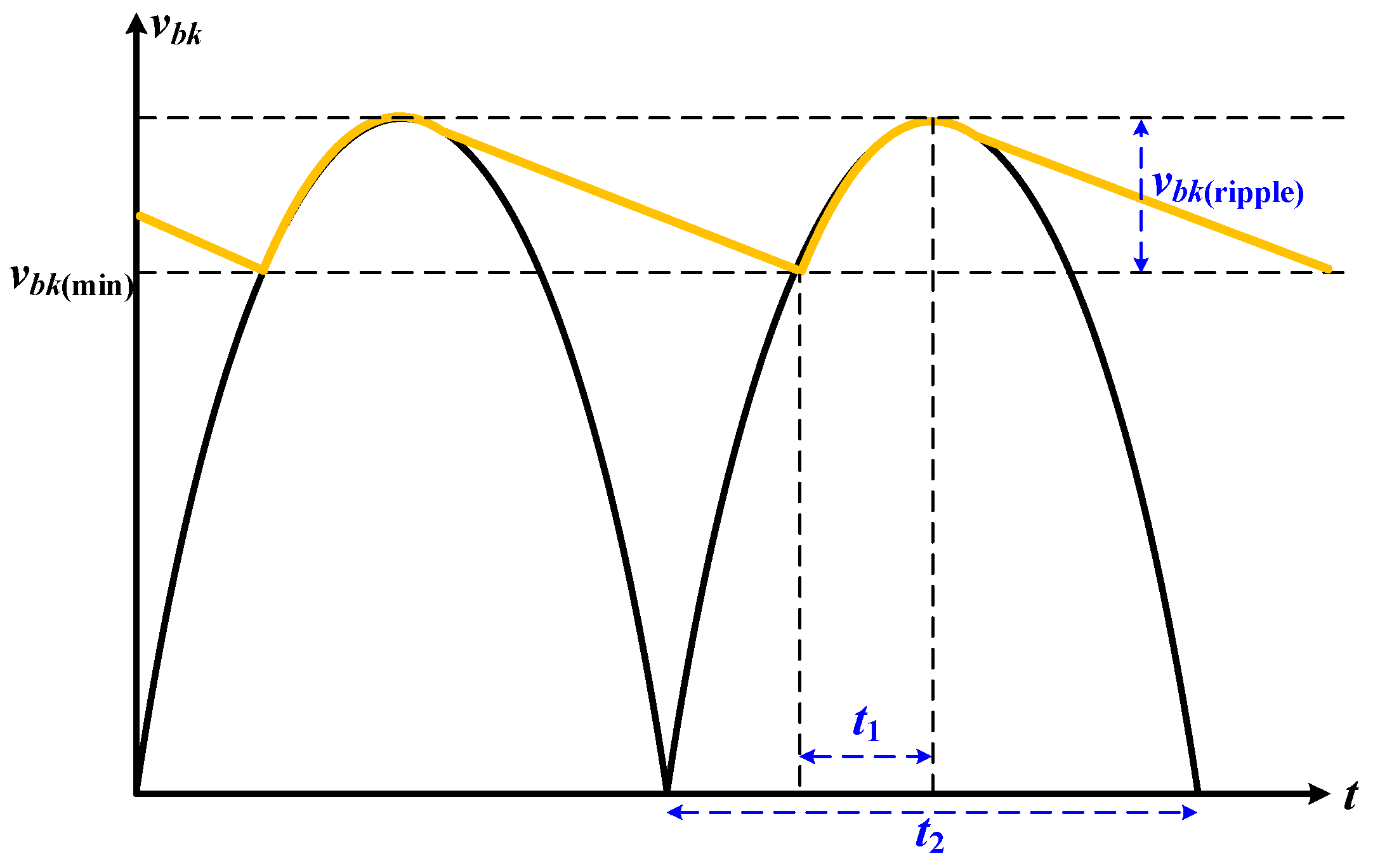
2.7. Input Filter Capacitor
When the QR-flyback converter is used as a DC–DC converter, the input AC power can be filtered by a capacitor after passing through a full-wave rectifier to obtain an input DC voltage. However, input DC voltage has a voltage ripple
vbk(ripple), as shown in
Figure 3. In
Figure 3, the cycle ratio
Dbulk =
t1/
t2 during the input filter capacitor charging is set to 0.2 [
20].
Moreover, the voltage ripple on the input filter capacitor was set to the maximum input AC voltage of 10% (
vac(max) = 140
× 10% ≅ 20 V); therefore, the minimum voltage across the filter capacitor
vbk(min) =
vac(pk,min) − 20 V = 120 V − 20 V = 100 V. Furthermore, according to [
21], the minimum voltage of the input filter capacitor can be expressed as:
which can be written as:
where
fline is the frequency of the input AC power source. Substitution of
vbk(min) = 100 V,
Dbulk = 0.2,
Pin(max) = 70 W,
vac(pk,min) = 120 V, and
fline = 60 Hz into (16) can obtain
Cin = 49.65 μF. However, the QR-flyback converter in this study was used as an AC/DC converter, and
Cin was used as a high-frequency filter; therefore,
Cin can choose a capacitance value 200 times smaller than 49.65 μF [
16]. In this study, the
Cin = 220 nF was chosen with the withstand voltage of 630 V (this withstand voltage was greater than
vac(pk,max) = 198 V) in the practical application.
3. Experimental Results
In this study, the experimental voltage and current measurements are shown in
Figure 1, including input AC voltage
vac, input AC current
iin, full-wave rectification voltage
vbk, transformer secondary-side current
isec, output voltage
Vout, output current
Iout, MOSFET drain-source voltage
vds, MOSFET gate source-voltage
vgs, and control voltage
Vctrl.
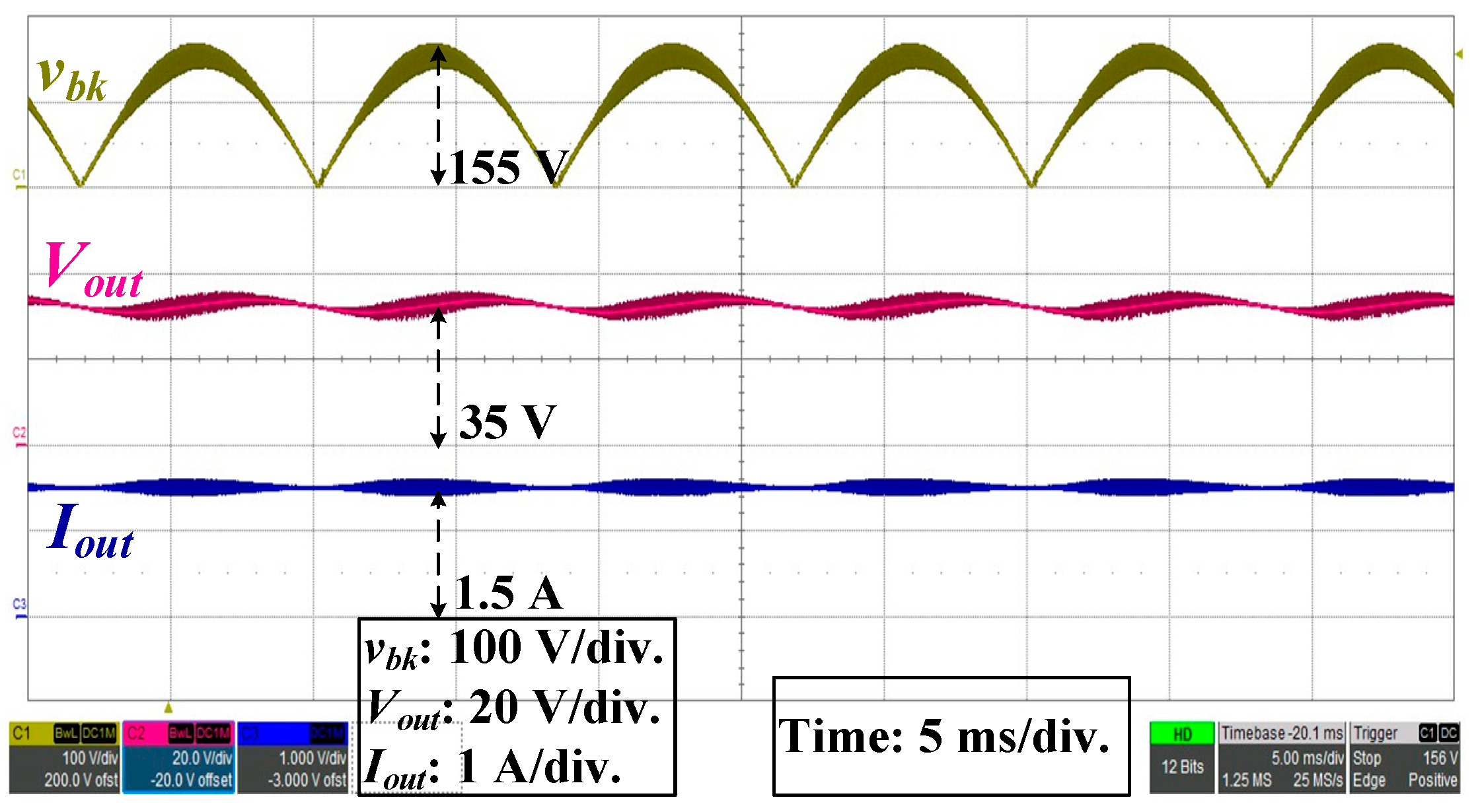
To confirm that the QR-flyback converter can output the rated voltage and current under the input AC condition, the peak value of
vbk was 155 V (110 V
rms),
Vout = 35 V, and
Iout = 1.5 A, as shown in
Figure 4.
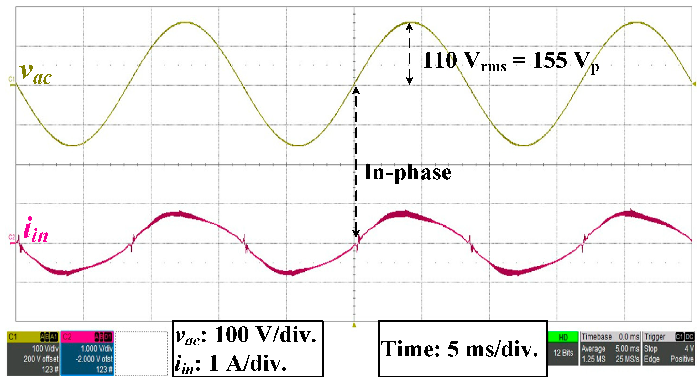
Under the full-load operation and
vac = 110 V
rms,
vac and
iin measurement waveforms are shown in
Figure 5. Waveforms of
vac and
iin were in-phase, which verified that the QR-flyback converter designed in this study achieved the power factor correction.
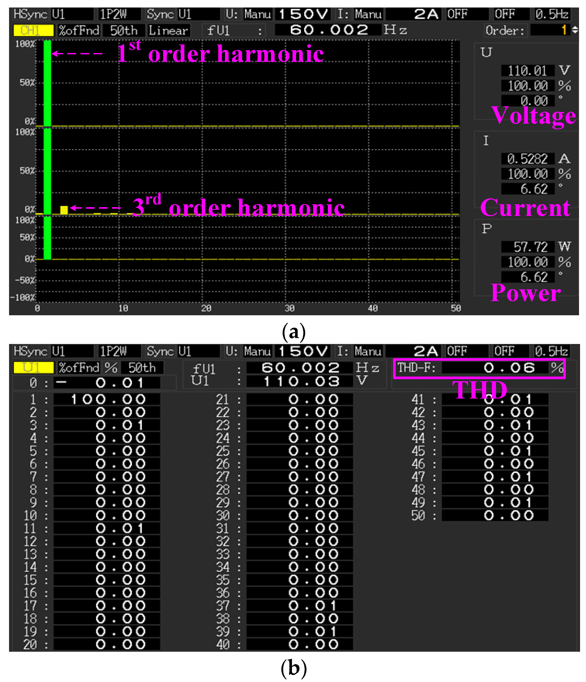
The power analyzer (PW3390, HIOKI E.E. Corp., Nagano, Japan) was used to measure the harmonic distortion rate. Under the full-load operation and
vac = 110 V
rms, the fifth-order harmonic histogram and harmonic record table are shown in
Figure 6. In
Figure 6a, the voltage, current, and power generated the maximum harmonic in the first (1st)-order; the current produced odd harmonics above the third (3rd)-order, whose values were low.
Figure 6b recorded that the THD percentage was 0.06%, which addressed the IEC 61000-3-2 Class-C standard [
22].
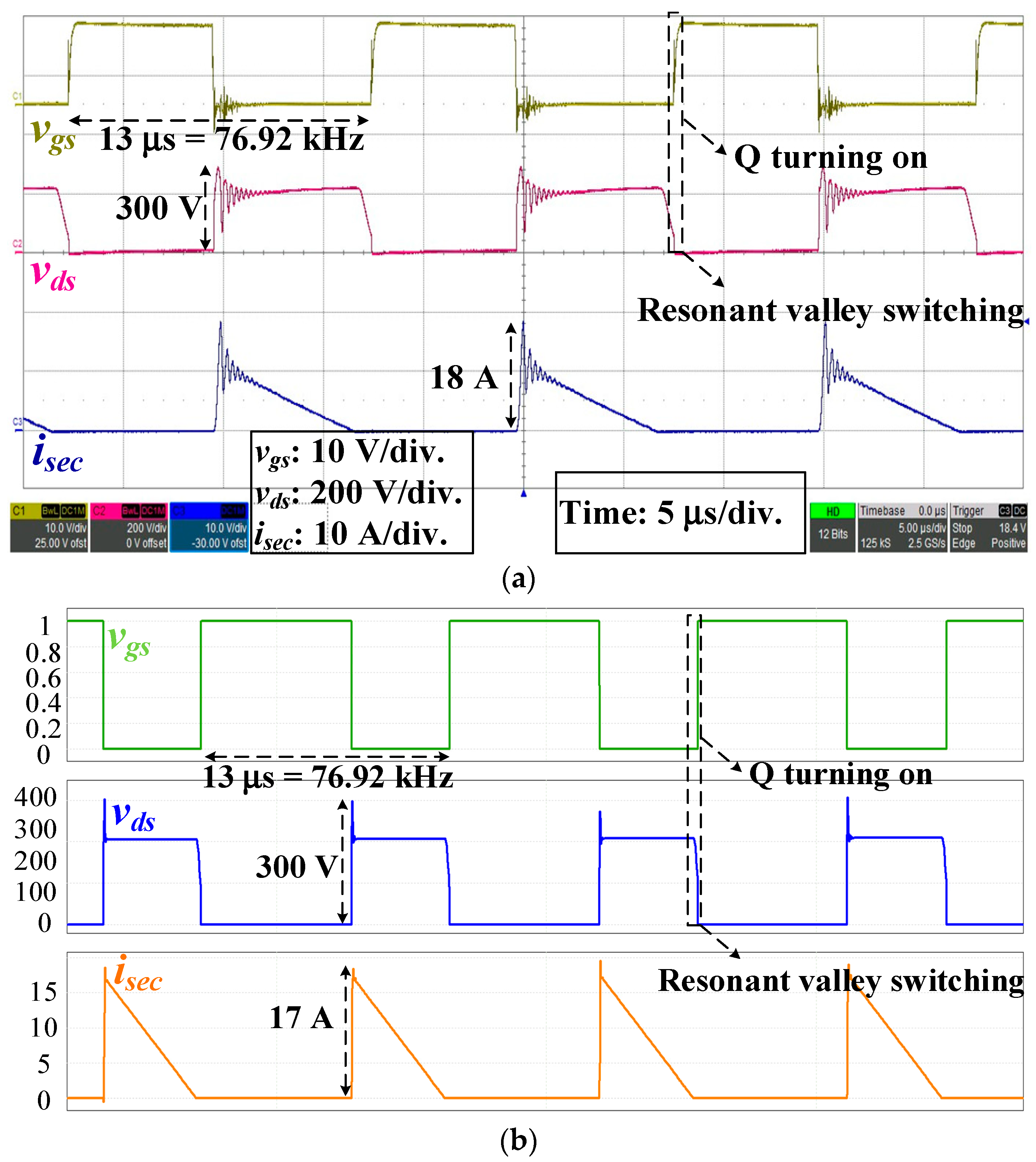
Under the full load operation and
vac = 85 V
rms, the experiment and simulation waveforms of
vgs,
vds and
isec are shown in
Figure 7. The operating frequencies of
vgs were 76.92 kHz (experiment) and 78.13 kHz (simulation), and the highest voltages of
vds were 300 V (experiment) and 300 V (simulation), respectively.
vgs was changed at the resonant valley of
vds, and the MOSFET switch was turned on. The PSIM software was used for the simulation. Moreover, the peak currents of
isec were 18 A (experiment) and 17 A (simulation), respectively; the result of
isec based on (13) was 13 A.
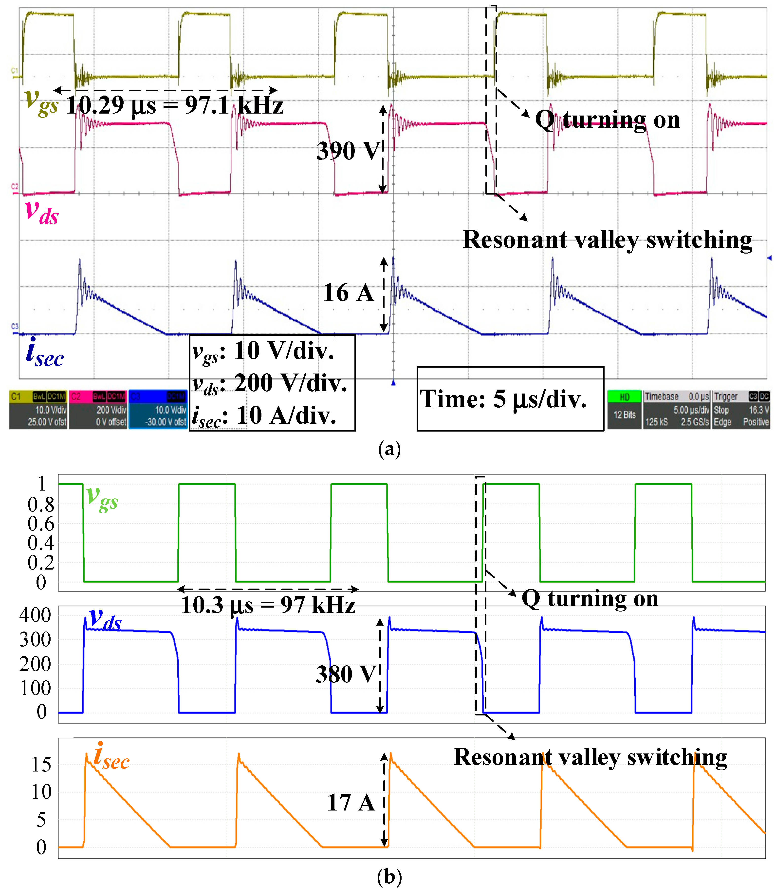
Under the full load operation and
vac = 140 V
rms, the experiment and simulation waveforms of
vgs,
vds and
isec are shown in
Figure 8. The operating frequencies of
vgs were 97.1 kHz (experiment) and 97 kHz (simulation), respectively; the highest voltages of
vds were 390 V (experiment) and 380 V (simulation), respectively.
vgs was changed at the resonant valley of
vds, and the MOSFET switch was turned on. Moreover, the peak currents of
isec were 16 A (experiment) and 17 A (simulation), respectively.
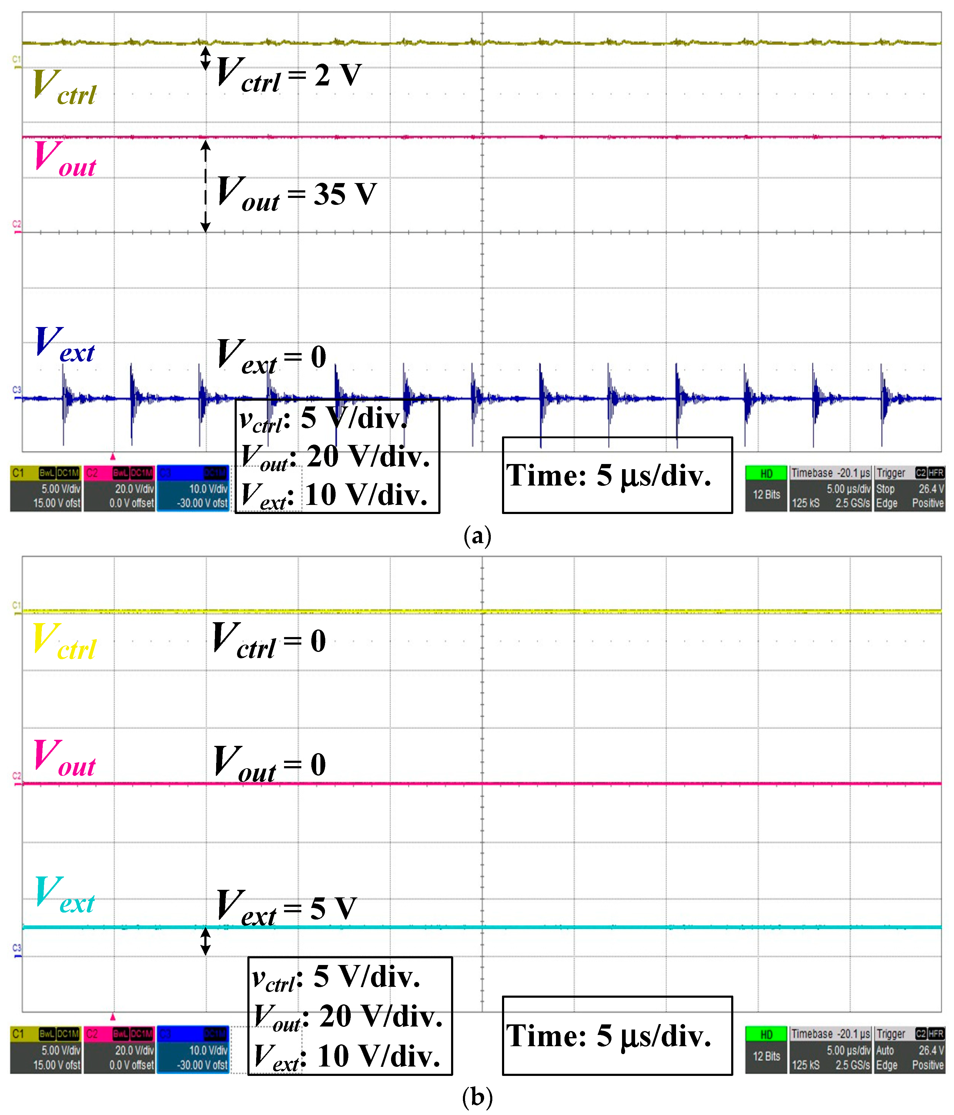
The external control signal
Vext (
Figure 3) was used to control the
Vctrl (
Figure 3) voltage level of the PWM control chip, and then
Vout of the QR-flyback converter can be controlled, as shown in
Figure 9. In
Figure 9a, when
Vext = 0,
Vctrl = 2 V, and
Vout = 35 V, this experiment represented the fact that the bright and extinguishable control circuit enabled the QR-flyback converter to drive the LED array streetlamp at
Vout = 35 V; therefore, the LED array streetlamp could be lighted. In
Figure 9b, when
Vext = 5 V,
Vctrl = 0, and
Vout = 0, this experiment represented the fact that the bright and extinguishable control circuit disabled the output voltage of the QR-flyback converter; therefore, the LED array streetlamp was dimmed.
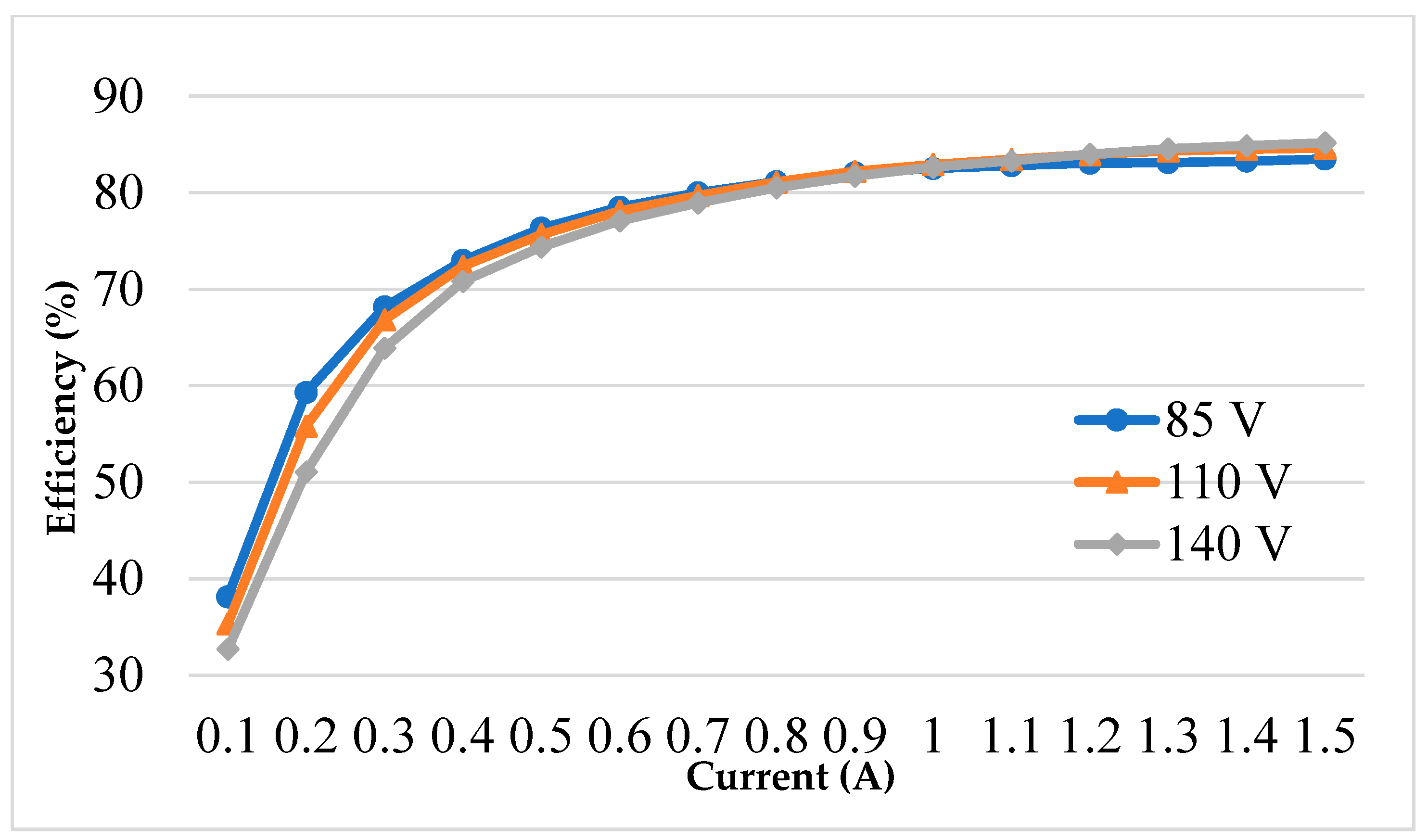
At the different
vac (85 to 140 V
rms),
Iout was changed from 0.1 to 1.5 A, the efficiency measurements were recorded in
Figure 10. The minimum efficiency was about 32% under the
vac = 140 V
rms and
Iout = 0.1 A; the maximum efficiency was about 85% under the
vac = 140 V
rms and
Iout = 1.5 A.
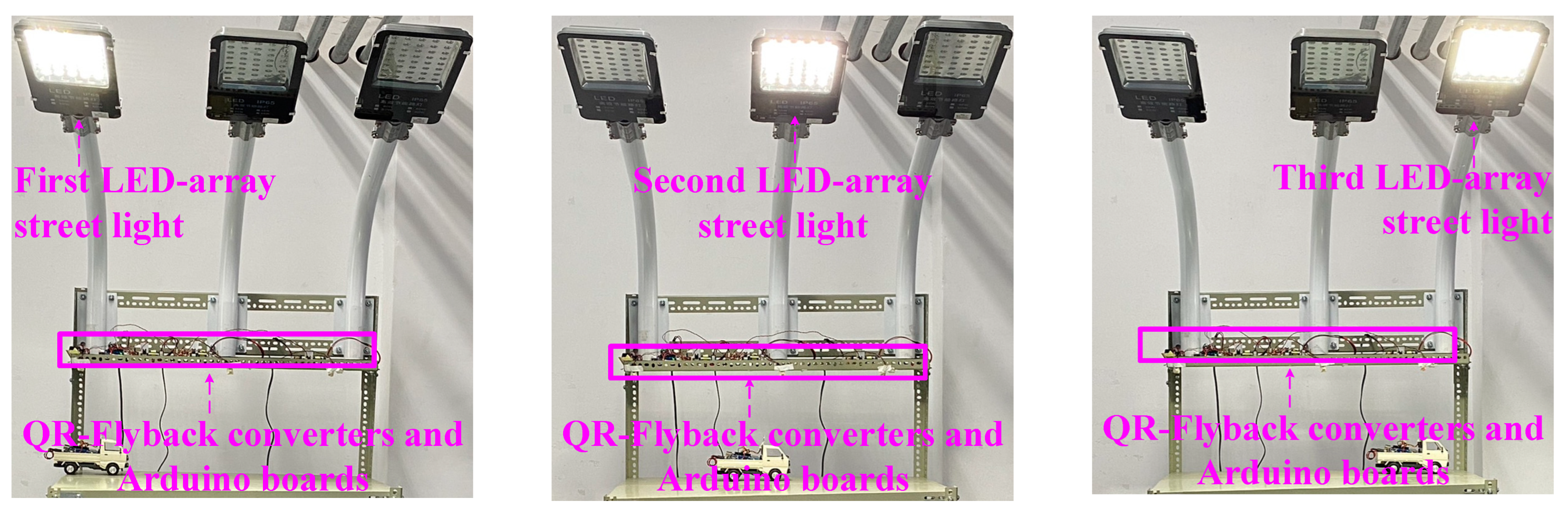
Vext (
Figure 1 and
Figure 9) was generated by the Arduino development board and combined with the QR-flyback converter to drive the LED array streetlamp system, as shown in
Figure 11. In
Figure 11, the three LED array streetlamps were controlled achieving bright and extinguishable operations at different times, when the model car moved to different positions.
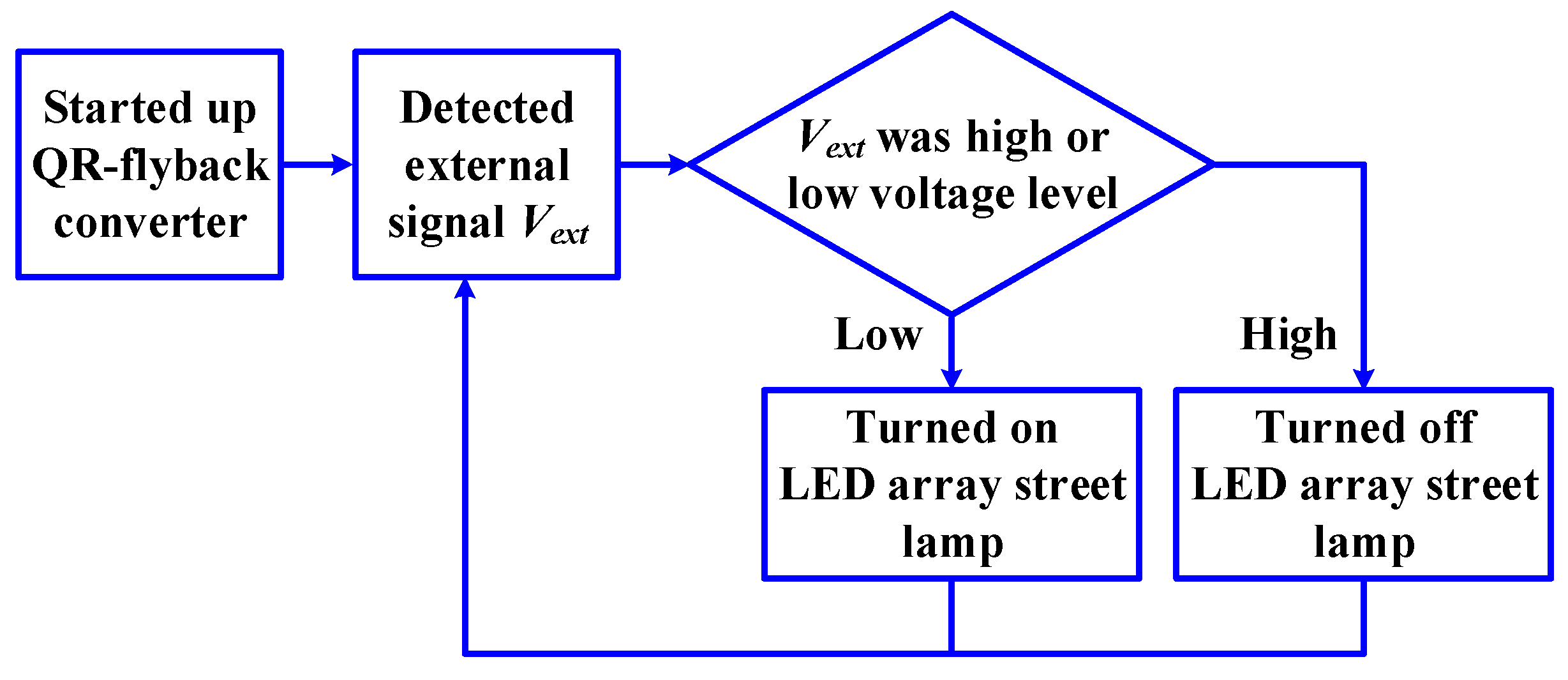
The implement block diagram of the LED array streetlamp is depicted in
Figure 12, its operation described as follows:
The QR-flyback converter was started up.
The external signal Vext was detected to control the bright and extinguishable control circuit.
When Vext was a low voltage level, the LED array streetlamp employed the bright operation; when Vext was a high voltage level, the LED array streetlamp employed the extinguishable operation.


