1. Introduction
Insulated Gate Bipolar Transistor (IGBT) is the core device in power electronic devices used for electric energy conversion and circuit control [
1,
2,
3]. Various IGBT structures and techniques have been proposed and studied, including the field stop IGBT (FS-IGBT) [
4], injection enhanced gate transistor (IEGT) [
5] and carrier stored trench-gate bipolar transistor (CSTBT) [
6]. With IGBT discrete devices and IGBT modules having an output power of up to 10 MW, they are widely utilized in high-voltage systems of Electric Vehicle, such as the main drive inverter, on-board charger (OBC), battery management system, on-board air conditioning control system, steering and other high-voltage auxiliary systems. In addition, IGBT is extensively employed in DC and AC charging piles, making them the cornerstone of the Electric Vehicle ecosystem.
For modern electronic systems represented by Electric Vehicles, higher operating frequency and higher power output are essential design goals. In the power converter system of Electric Vehicles (e.g., DC/DC converter, DC-to-DC inverter and the electronic power transformer), increasing the operating frequency can significantly benefit the system by reducing its volume, eliminating total harmonic distortion and improving power quality [
7,
8].
However, IGBT is still bottlenecked by technical and physical limitations, such as the unique trailing current and resulting switching loss that restrict the switching frequency to below 20 kHz [
9,
10,
11]. Among the IGBTs mentioned above, CSTBT stands out as a promising candidate for the next-generation power electronics due to its ability to significantly reduce the on-state voltage while improving the carrier distribution in trench IGBT [
12,
13,
14].
In a typical CSTBT, an additional carrier storage (CS) layer with a higher doping concentration is located between the P-type well region (P-body) and the N-drift region. In the on-state, the CS layer acts as a higher potential barrier that blocks holes from being collected by the emitter, leading to hole accumulation in the drift region near emitter side [
15,
16]. Accordingly, this causes a considerable number of electrons to be injected through the emitter, maintaining electrical neutrality and increasing the carrier concentration [
17,
18].
The switching frequency of optimized IGBTs is limited to 20 kHz to 40 kHz, which falls short of the desired 100 kHz, resulting in a tradeoff between high power and high frequency [
19,
20,
21].
Therefore, improving the switching performance of IGBT has become a highly concerned issue, with two primary limiting factors listed below:
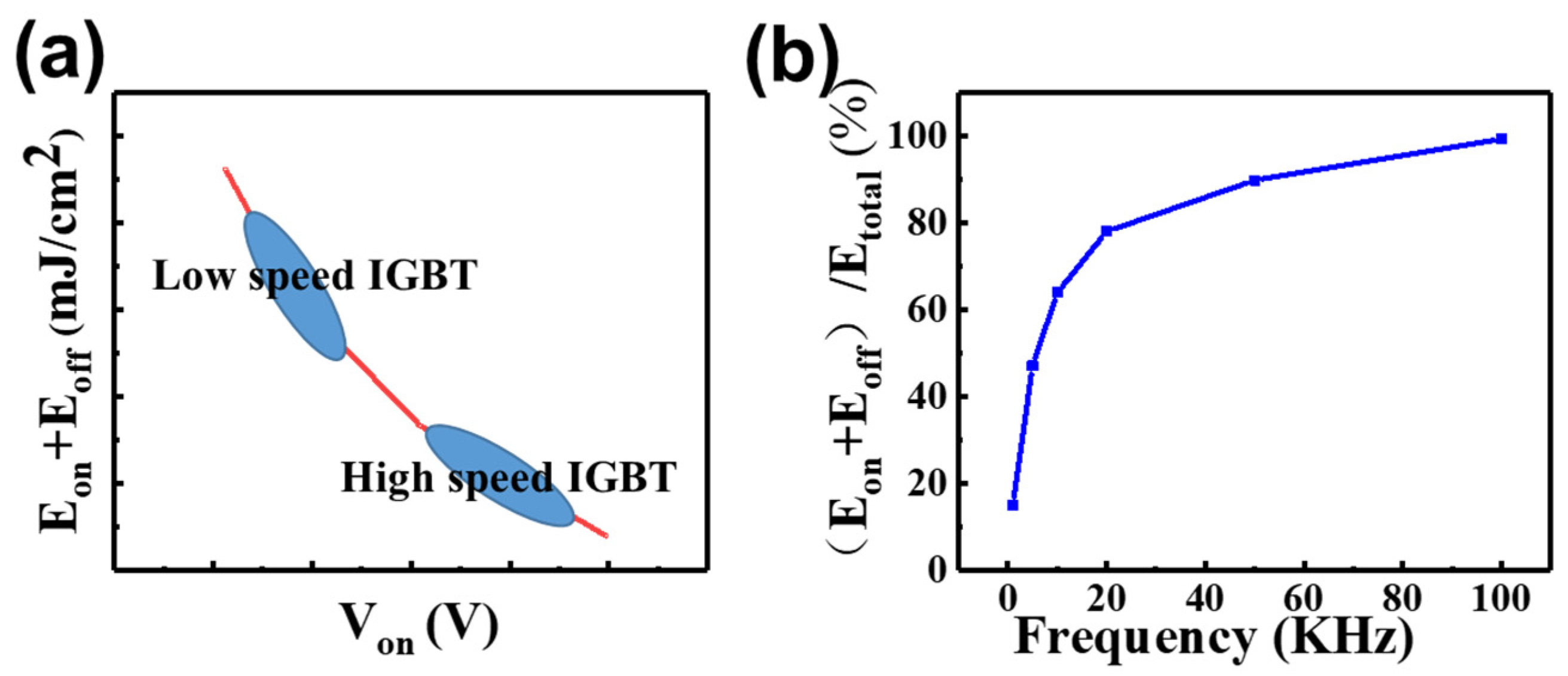
Switching frequency refers to the number of times the IGBT is switched on and off within a second. Under the specified bus voltage and current, IGBT will generate power loss every time it switches. As the switching frequency increases, so does the power loss and temperature rise, which could lead to IGBT failure if the temperature exceeds the upper limit. The total power losses of an IGBT chip are typically composed of turn-on loss (Eon), turn-off loss (Eoff) and conduction loss, and are proportional to the product of frequency and switching loss (Eoff + Eon).
In high frequency switching applications above 20 kHz, the reduction of switching loss becomes crucial, as it accounts for the majority of the total power consumption (above 60%), as shown in
Figure 1b. In order to reduce the total power consumption under the switching frequency of 20~50 kHz, IGBT chip performance must be set at the position of high V
on, low E
on and E
off, like High speed IGBT in
Figure 1a.
Currently, shield gate technology (SGT) is a promising way to reduce switching loss by decreasing Qg. However, the grounded bottom electrode in SGT increases channel resistance, leading to a serious impact on Von and a corresponding rise in conduction loss.
In this work, we propose a CSTBT device with a forward DC bias shield gate and hole path (DC-CSTBT). The characteristics of low Von, low Eon, low Eoff and high breakdown voltage are demonstrated simultaneously. The proposed device only made minor changes on the basis of conventional CSTBT and offers a simple and easy-to-implement structure and process.
2. Structure and Process Flow
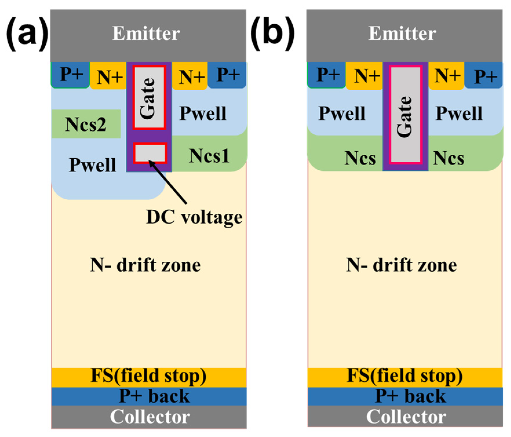
The schematic diagram of the proposed DC-CSTBT is shown in
Figure 2a. Compared with the conventional CSTBT shown in
Figure 2b, both devices have the same doping profile except for an extra N-type carrier storage layer (CS2).
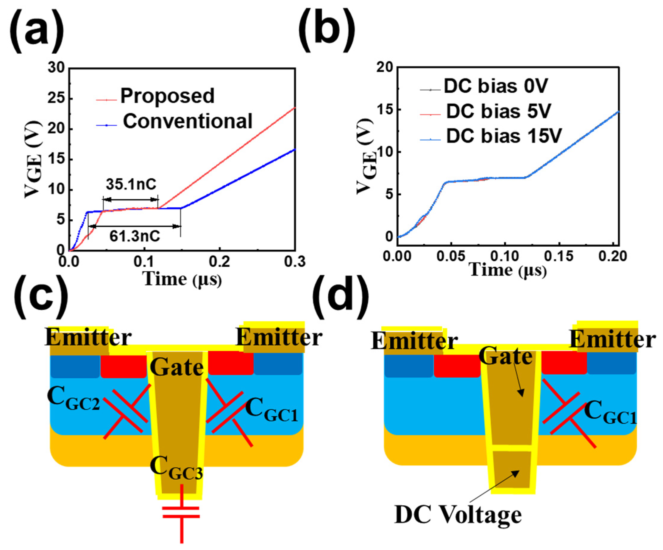
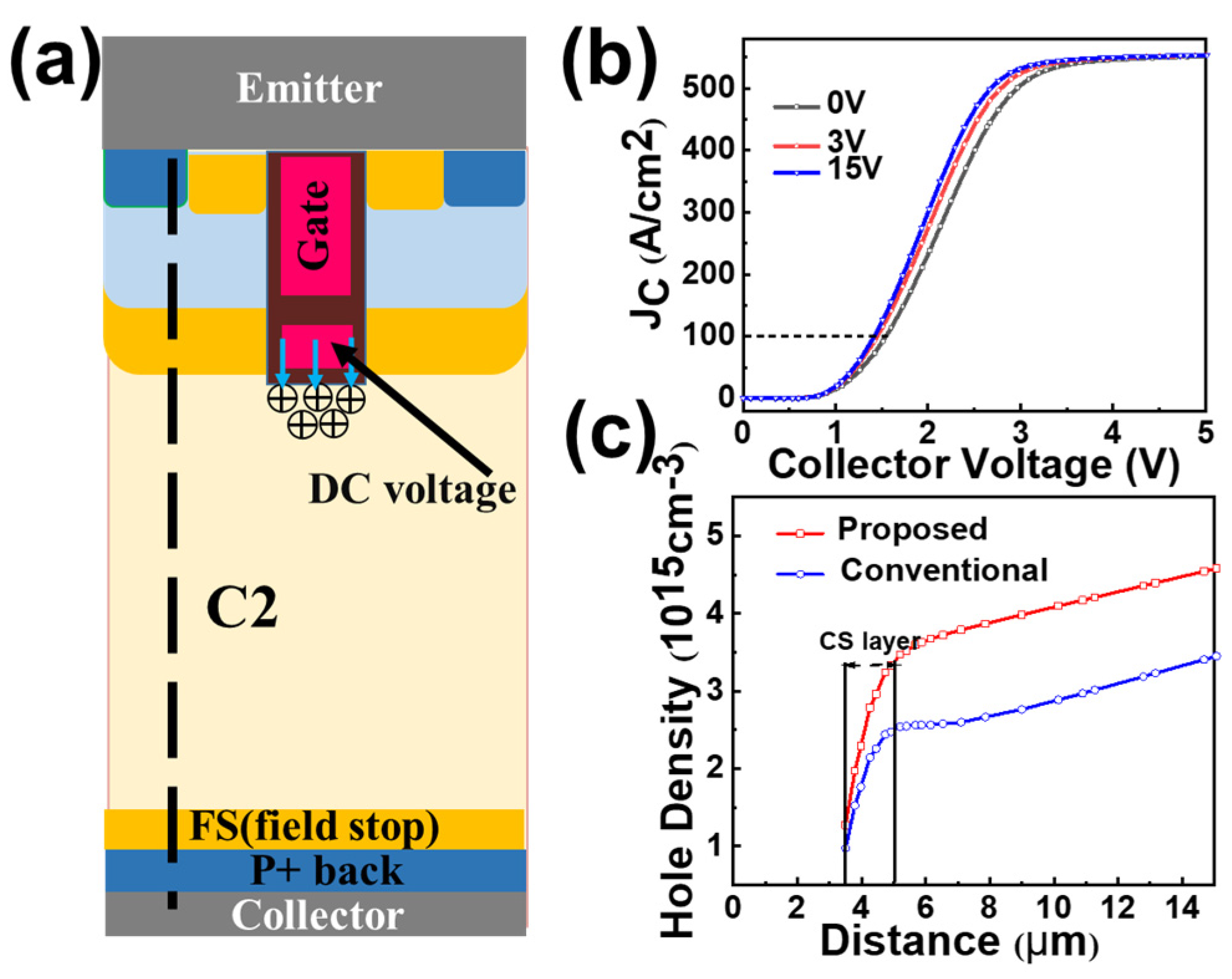
In the proposed DC-CSTBT, the trench gate is split into two parts, including the upper and deeper parts. The upper part is connected to the gate control signal, controlling the turning on and off of the device. The deeper shield trench gate is connected to a positive DC bias. Generally, the DC bias value is the same as the gate saturation turn-on voltage, and there is no need to add the additional output of the driving circuit.
The CS2 region on the left is achieved by additional lithography and ion implantation. There is a gap between the trench and the CS2, and the state (on/off) of this hole path is completely controlled by the trench gate voltage. In the on state, the hole channel is closed, and the gap is inverted and acts as a whole CS storage layer with a CS2 layer. As the CS2 locates away from the bottom of the trench, its doping concentration is high to reduce V
on without blocking characteristic deterioration.
Table 1 shows the major structural parameters of the proposed device.
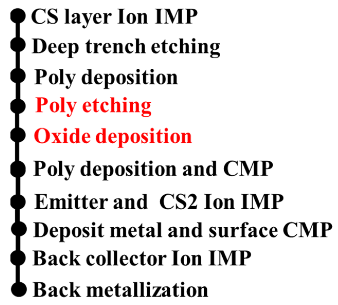
The split trench gate technology is compatible with the current manufacturing process. The process flow of the device is shown in
Figure 3. The main process steps include epitaxial layer formation, ion implantation, trench etching, polysilicon deposition and etching, oxide layer formation, etc. Two additional processes compared with the conventional CSTBT process are highlighted in red, namely the polysilicon etching and the oxide layer deposition.
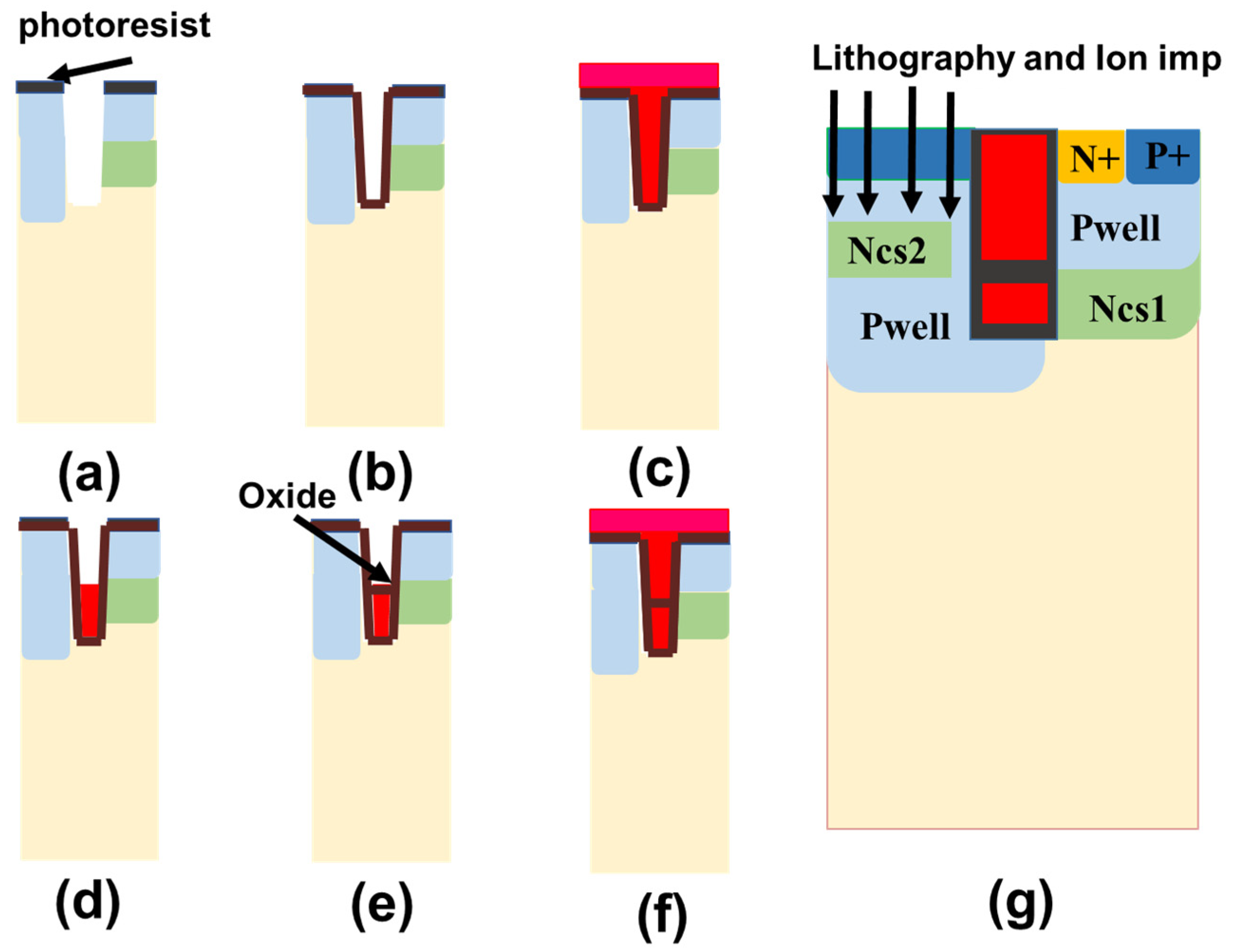
In addition, the detailed device process of split gate formation is shown in
Figure 4a–f below. After deep trench etching (
Figure 4a), an oxide (
Figure 4b) and a very thick polysilicon (
Figure 4c) is deposited in the trench. Then, part of the polysilicon is etched (
Figure 4d), and only the bottom part as a shield gate is left. Subsequently, an oxide layer is deposited to complete the isolation of the upper and lower split gates (
Figure 4e). Finally, polysilicon is deposited into the trench to form the split gate (
Figure 4f). The split gate at the bottom serves as the DC bias shielding gate in the paper.
Figure 4g shows the formation of CS2 on the left. A high-energy ion injection is added after an emitter injection, and the distribution of the CS2 layer is defined by mask.
Despite the slight increase in device fabrication complexity or cost associated with the proposed DC bias shielding approach, the process steps are completely consistent with those of existing trench IGBT devices. Additionally, the inclusion of a DC bias shield gate necessitates only minimal alterations to the driving circuit and requires the addition of only one lithography mask. This device has a simple structure and low cost, with great potential for practical applications.
3. Simulation Results and Discussion
The device model is established by the Sentaurus Technology Computer-Aided Design (TCAD) simulation, and the process conditions are based on the SMIC 0.18 µm process node. The following four aspects of optimization brought by DC bias shielding are introduced. The structures contrasted below include a conventional CSTBT, a conventional shield CSTBT with a grounded shield gate (Con-SGCSTBT), DC-CSTBT, referring to CSTBT without a split gate, a split gate CSTBT with grounded shield gate and the proposed DC bias CSTBT, respectively.
- A.
Low Eon
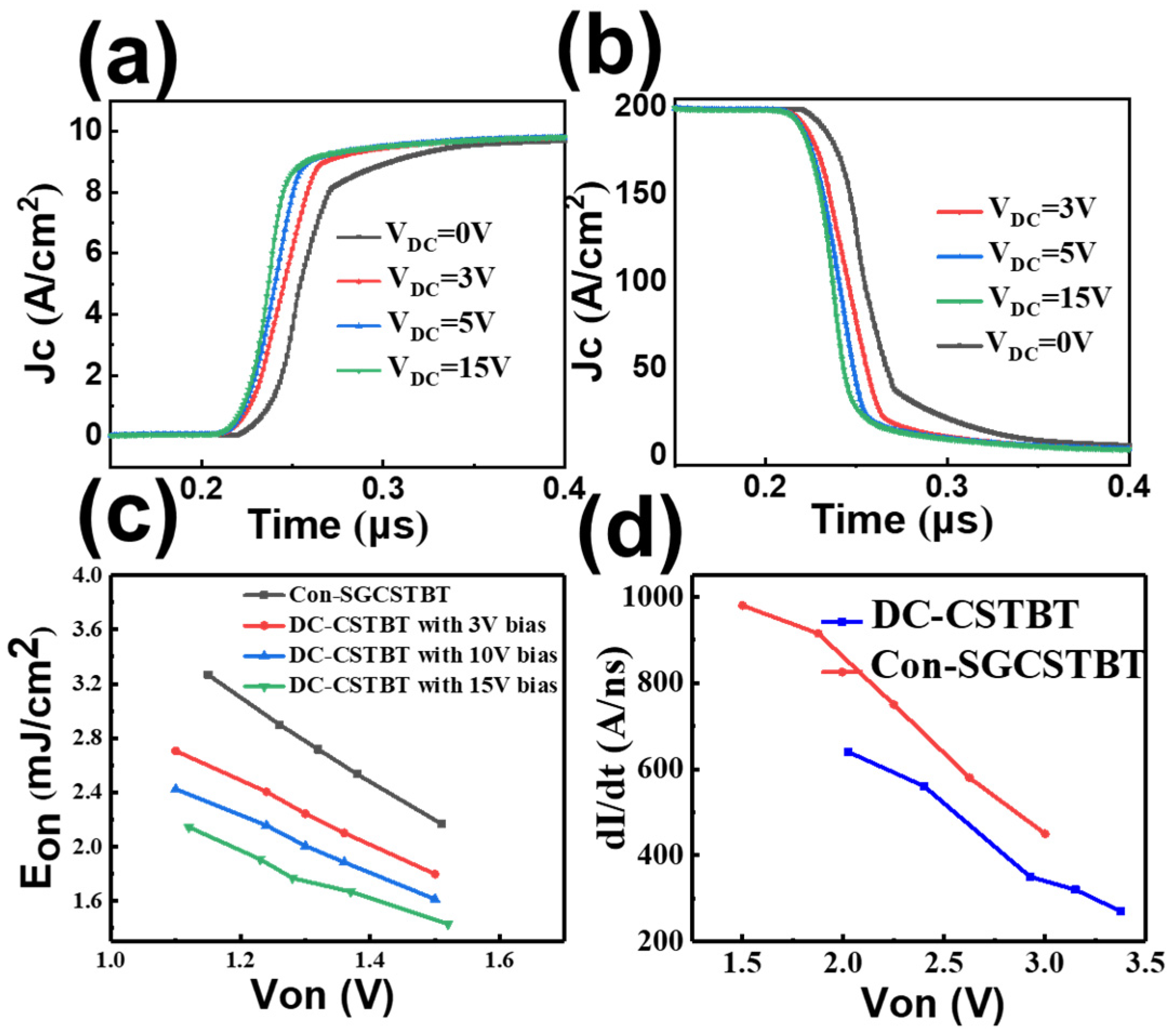
There are two factors contributing to the low Eon. Firstly, the SGT gate structure reduces the Miller capacitance, which helps to decrease the Eon. The Miller effect induces the formation of a platform voltage when driving the trench gate, which subsequently prolongs switching time and heightens switching loss. These consequences can have profoundly detrimental effects on the normal operation of the IGBT. Secondly, the shield gate DC bias technology accelerates the formation of conductive channels, further reducing the Eon.
(1) low QGC
In the conventional CSTBT structure, the whole C
GC is composed of three parts, as depicted in
Figure 5c; namely, C
GC1, C
GC2 and C
GC3. C
GC1 and C
GC2 are mainly related to gate oxide thickness and the coupling area between trench and collector. Among these three parts, C
CG3 is the most dominant factor. Compared with a conventional CSTBT, the deeper trench of the proposed device is DC biased (equivalent to AC ground), resulting in a smaller coupling area between the gate and collector. The charging time of the Miller capacitor is reduced by 42.7% in the proposed DC-CSTBT compared with the conventional CSTBT. Q
GC is reduced from 61.3 nC to 35.1 nC, and the Miller capacitance of the proposed device, equivalently, is decreased from 8.636 nF/cm
2 to 2.57 nF/cm
2. The reduction in Miller capacitance is mainly transformed into C
GE. The simulation results indicate that the Q
GC of the proposed device remains constant under a different DC bias, as depicted in
Figure 5b. Therefore, a higher DC bias can enhance the carrier storage effect without deteriorating the Miller effect.
(2) Faster turn-on by forward biased bottom inversion channel
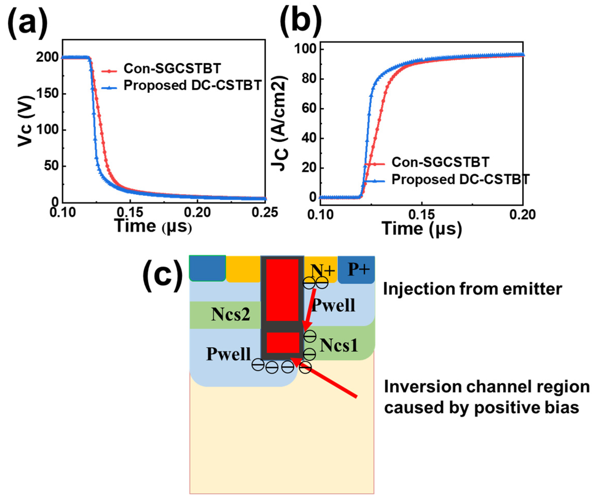
Con-SGCSTBT will bring the problem of excessive Von. To address this, the improved DC-CSTBT is proposed here.
Figure 6 shows the turn-on curve of the proposed device under a clamped load. The collector current voltage and collector current of the proposed device is swifter than C
on-SGCSTBT, as depicted in
Figure 6a,b. This improvement can be attributed to the inverse channel forward formed by the DC voltage at the trench bottom rather than the grounded deep trench. The formation of a conductive channel is accelerated and the turn-on process is sped up effectively by the DC biasing technique.
The turn-on process of the IGBT is as follows. First, a positive bias is applied at the trench, which inverts the P-base region to form an N channel. Then, the emitter releases electrons into the drift region through this channel, leading to the potential drop in the drift region. When the potential is low to a certain threshold, the collector PN junction conducts forward, and holes are injected into the N-region; conductance modulation effect starts.
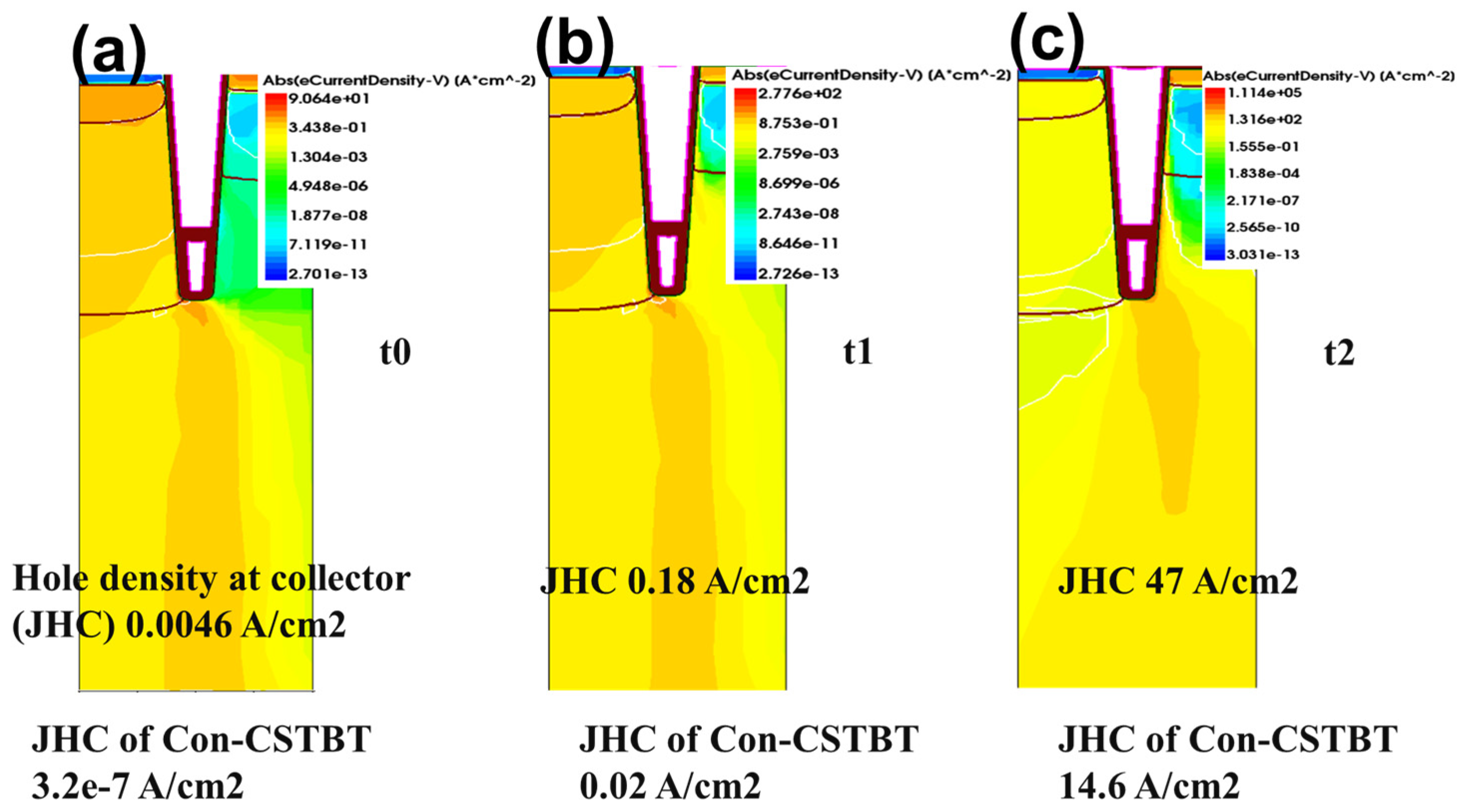
Figure 7 shows the distribution of electron current during the turn-on state. Large electron currents flowing to the drift region can be clearly seen at the trench bottom. The mechanism can be explained as follows. There exists a DC bias at the shield gate and a corresponding electric field pointing from the trench bottom to the emitter. Consequently, electrons in the emitter are injected through the inversion layer around the shield gate, resulting in a decrease in the N-drift potential.
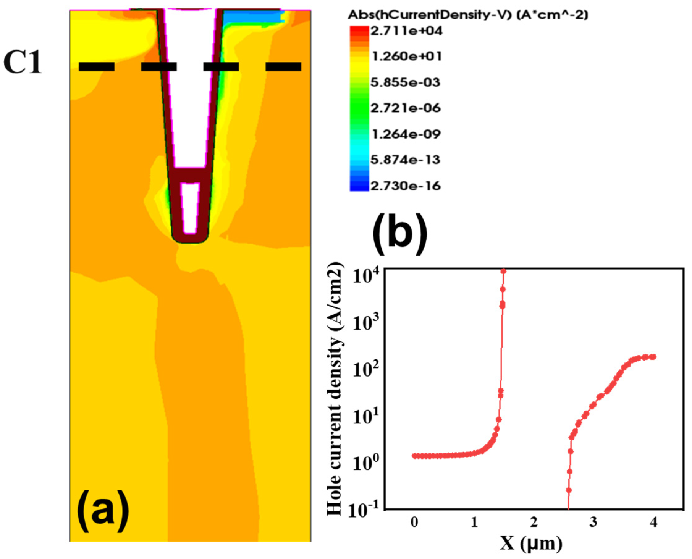
Moreover, the hole current density at the collector region is marked, which can further compare the collector injection speed, as illustrated in
Figure 7a–c. At t
0, the hole current density at the collector (J
CH) of DC-CSTBT is 10
4 larger than that of the normal grounded shield gate. At t
1, J
CH of DC-CSTBT is also nine times larger. Until t
2, both reach an order of magnitude of 47 A/cm
2 and 14.6 A/cm
2, respectively. It is further proved that the DC bias shield can speed up the device turn-on process.
Figure 8 shows the turn-on curve of the proposed DC-CSTBT (under various DC bias). It can be seen that the J
C of the DC-CSTBT with a higher DC voltage is much swifter. A higher DC bias contributes to a stronger electric field to promote the incident of electrons. In addition, during the turn-on process, dV/dt and dI/dt are significantly improved, and the turn-on loss can be reduced. The simulation results show that, compared with the C
on-SGCSTBT, the E
on of the proposed device can be reduced by 35.9%, from 3.2 mJ/cm
2 to 2.05 mJ/cm
2.
- B.
Low Eoff
Figure 9a illustrates the transient hole current distribution during the turn-off at t
1 (a period of time after the turn on time t
0) of the DC-CSTBT and hole current values along C
1. It can be seen that the highest hole current is concentrated at the designed hole path, reaching more than 1 × 10
4 A/cm
2 as depicted in
Figure 9b.
In the turn-off process, the inversed hole path recovers into the P-region with VG transferring to zero. Consequently, the accumulated holes in the drift region are swept out through the inversion layer around the hole path region, accelerating hole extraction to make the drift zone reach neutrality as soon as possible.
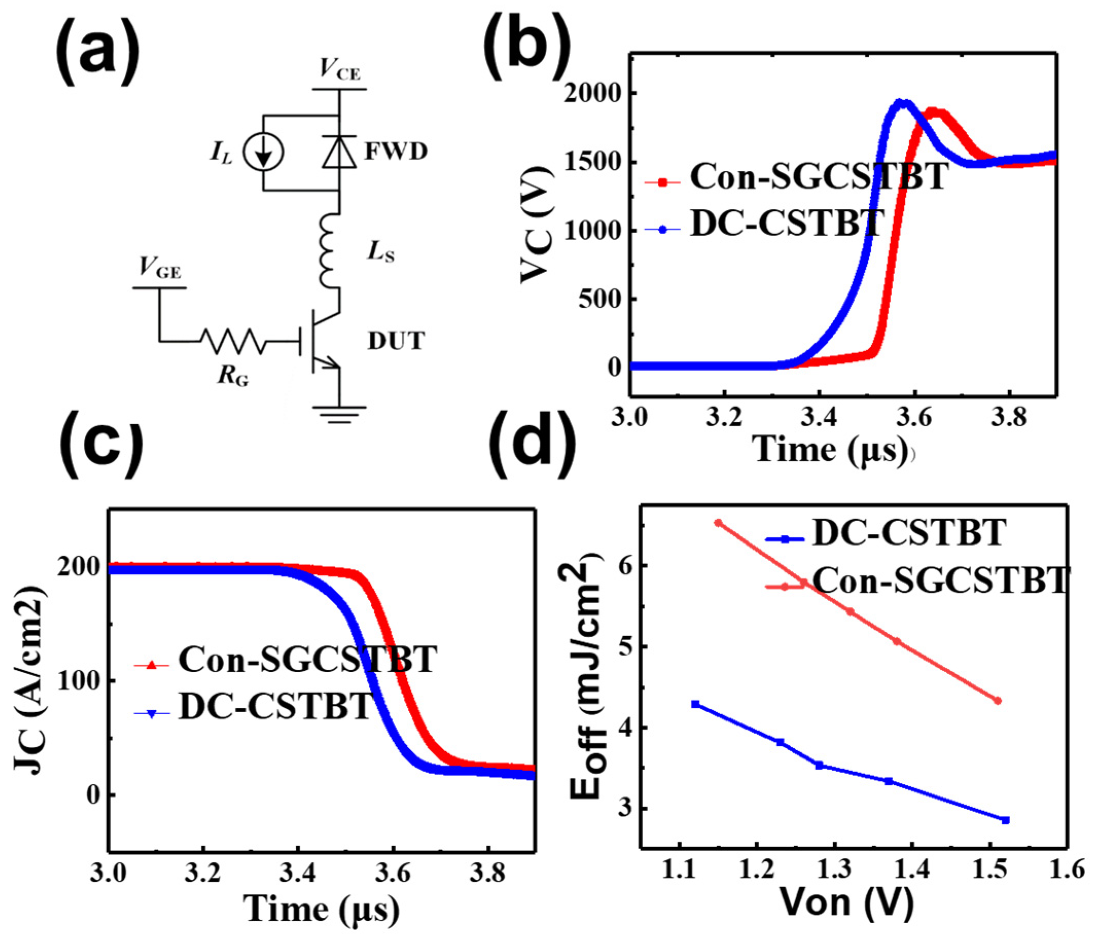
The mixed-mode, clamped, inductive switching simulation is performed to study the turn-off performance. The simulated devices are set to the same current of 10 A at the current density of 100 A/cm
2. The DC bus voltage (V
bus) is set to 1500 V. The load inductance L
c load is 1 mH and the circuit is shown in
Figure 10a. The gate voltage decreases from 15 to 0 V to turn off the device. The simulated turn-off process of C
on-SGCSTBT and the proposed DC-CSTBT (with same V
on of 1.5 V) are shown in
Figure 10b,c. Clearly, the T
off of the DC-CSTBT is much smaller than that of C
on-SGCSTBT, which indicates that the E
off of the proposed device is more excellent.
Figure 10d illustrates the relationship between E
off and V
on for the two different structures, after changing the peak P-collector doping concentration. Under V
on = 1.15 V, the E
off of the proposed DC-CSTBT is 6.5 mJ/cm
2, which is 36.1% lower than that of the C
on-SGCSTBT (4.15 mJ/cm
2). In addition, the switching loss, including E
on and E
off, are further compared, as shown below.
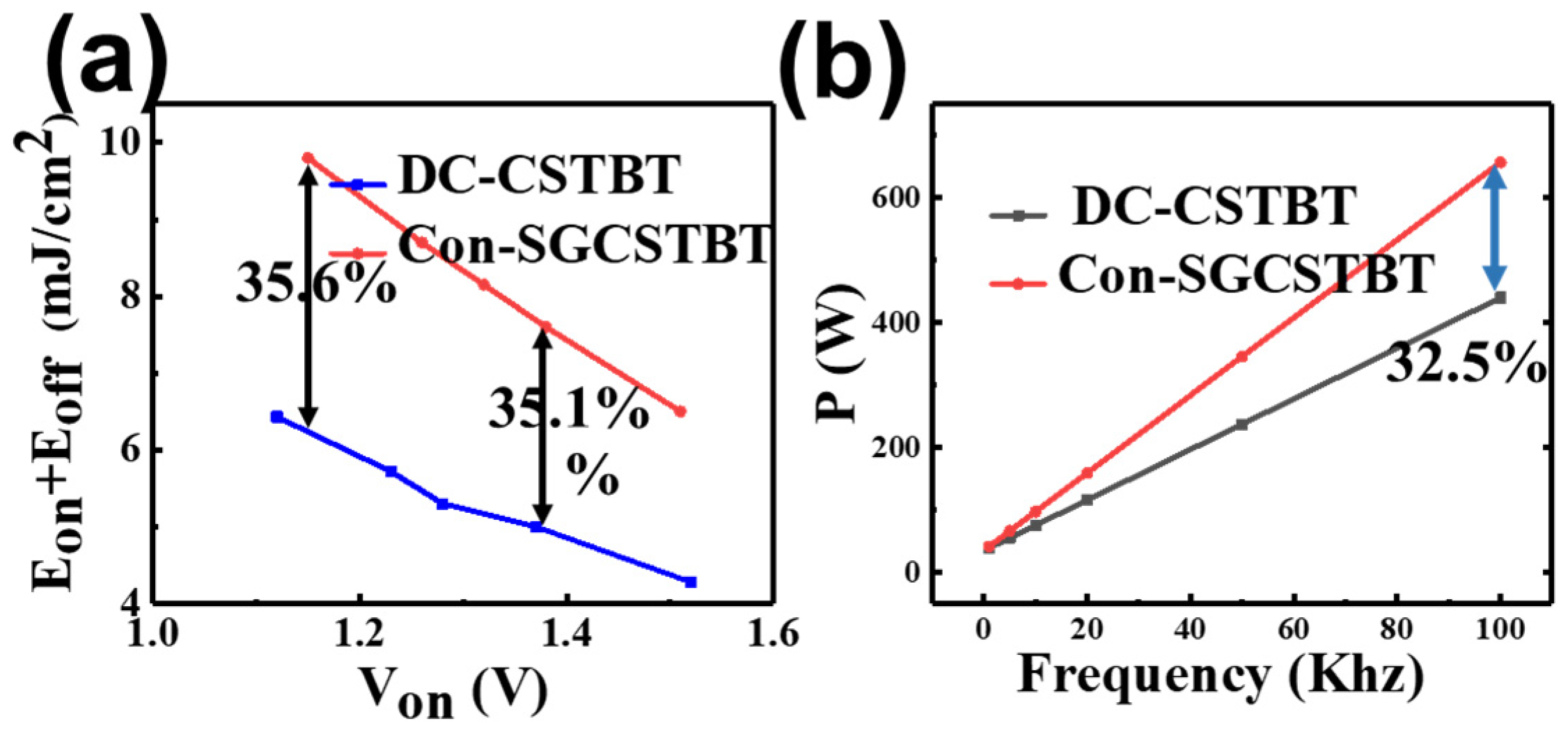
Figure 11 shows the tradeoff curves of V
on − (E
off + E
on) for the devices. It is observed that the tradeoff curves of DC-CSTBT is obviously more optimized than C
on-SGCSTBT. This is mainly due to the presence of both a hole path and emitter electron injection acceleration techniques, which improve turn-on and turn-off, respectively. For the same V
on 1.38 V, E
off + E
on of DC-CSTBT is decreased by 35.1% compared with the C
on-SGCSTBT. However, with the V
on of 1.14 V, this reduction percentage is still higher. Considering the same E
off + E
on of 6.4 mJ/cm
2, the V
on of the DC-CSTBT can be 25.8% lower than that of the C
on-SGCSTBT. Therefore, DC-CSTBT have a better tradeoff between V
on and E
off + E
on than C
on-SGCSTBT. Correspondingly, the calculated power loss in high-frequency switching applications (100 kHz) can be reduced by 32.5% as shown in
Figure 11b.
- C.
Blocking characteristics
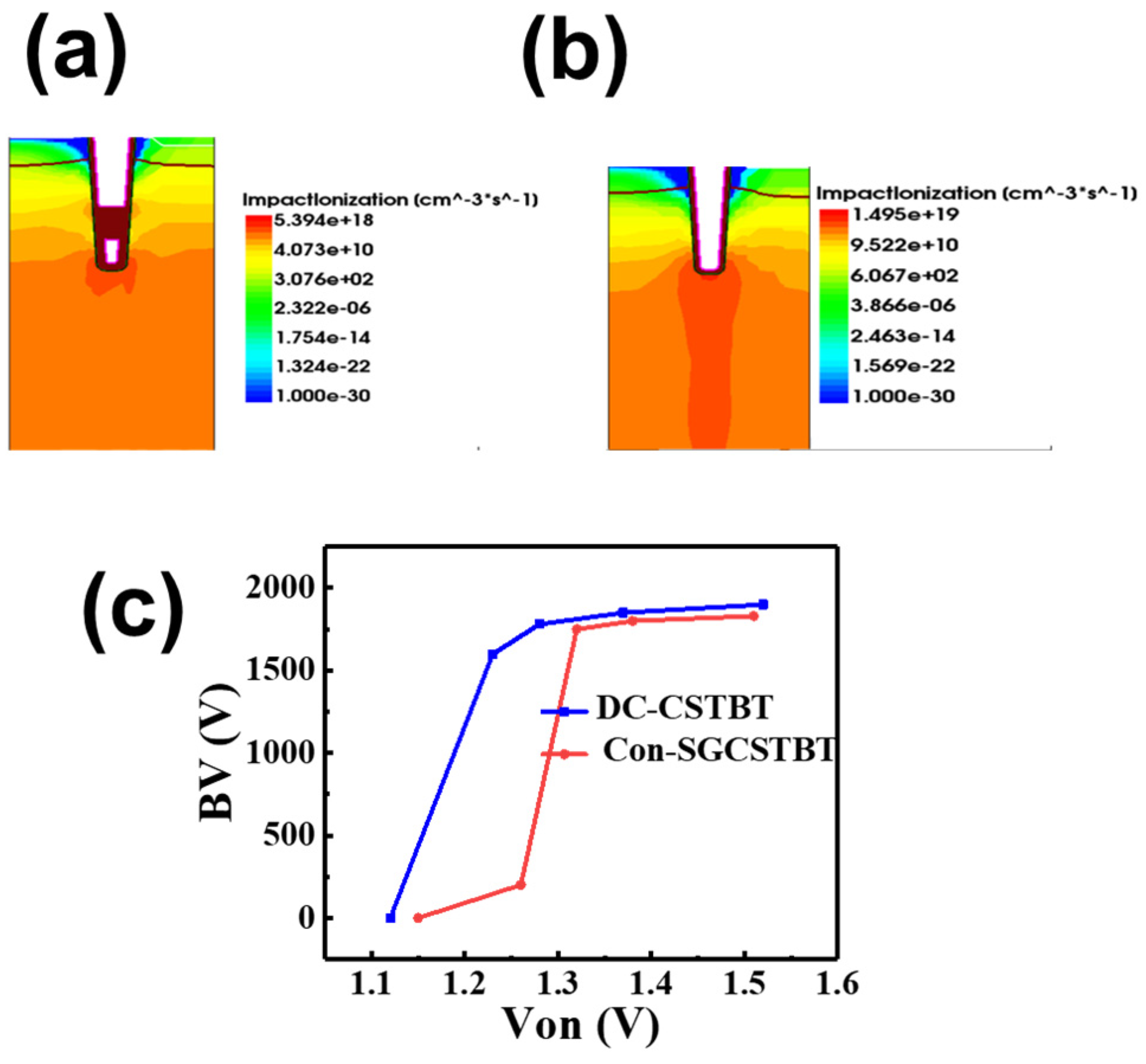
As mentioned above, the breakdown voltage of the trench IGBT is affected by the deep trench structure. The breakdown voltage of the trench IGBT is lower than that of the traditional planar type because of the pre-breakdown of trench bottom.
Especially with the introduction of the carrier enhancement layer, the electric field at the bottom becomes too concentrated. The reason for the high electric field is the largest potential difference at the trench bottom. The electric potential of the trench is 0 V, which is the lowest potential at the same depth in the drift region. Breakdown initially occurs at the bottom of the trench. Some structures have previously been proposed to attenuate the overly concentrated electric field, such as implanting the P-type doped well at the bottom. However, the conduction loss will increase significantly because of the drift zone resistance increase. To address this issue, the proposed DC bias device employs a deeper trench electrode connected with a forward DC bias to reduce the potential difference at the bottom trench by raising the potential at the shield gate, thus relieving the electric field at the bottom of the trench effectively.
Figure 12a,b show the impact ionization distribution under same reverse bias at 1800 V. It should be noted that C
on-SGCSTBT shows similar breakdown characteristics as a conventional CSTBT for the same electric field distribution at the trench bottom, while the proposed device can reduce the peak impact by about 50% compared with C
on-SGCSTBT.
Figure 12c illustrates the tradeoff relationship between BV and V
on of C
on-SGCSTBT and the proposed DC-CSTBT (by changing the doping concentration of the CS layer). Under the same V
on, the proposed device always has a higher BV because of the weakened electric field at the trench bottom. For C
on-SGCSTBT, the BV starts to decrease when V
on is smaller than 1.35 V (reduce the conduction pressure drop by increasing the concentration of CS). While the proposed device can maintain 1600 V withstand voltage until V
on is smaller than 1.2 V. The present device achieves a better tradeoff relationship.
- D.
Conduction characteristics
The forward DC bias at the deep shield trench repels positively charged holes because of mutual repulsion between positive charges, promoting the accumulation of holes near the trench bottom, as depicted in
Figure 13a. Therefore, a large number of holes accumulates at the emitter side. In order to maintain electrical neutrality, the emitter should emit a corresponding quantity of electrons. With the increase in carrier doping concentrations in the drift region, the on-resistance of the device is reduced.
Figure 13b shows the comparison of output characteristics of the proposed device under different forward DC voltages including 0 V, 3 V and 15 V. It is clear that V
on decreases with DC bias rises, as a higher DC voltage contributes to a stronger hole block effect.
Figure 13c compares the distributions of the hole carrier density along line C2 for DC-CSTBT and with a DC bias at collector current density J = 100 A/cm
2. As the DC bias at the deeper electrode only contributes to a higher hole carrier density near the emitter, only a little penalty in the switching losses will be added.
- E.
Other characteristics
Output characteristics, transfer characteristics and short circuit characteristics are also studied. Simulation results show that the JC–VG curve does not change, while the saturation current and short circuit characteristics are greatly optimized.
Figure 14a shows that the saturation current density is significantly reduced compared with C
on-SGCSTBT, since no current flows through the left half of the proposed DC-CSTBT. In addition,
Figure 14b shows the transfer characteristics (J
C–V
G curve) of C
on-SGCSTBT and the proposed device under the same V
on. The curve of both devices almost overlap, indicating that the proposed structure only optimizes the device characteristics by adding a DC bias shield structure, while preserving the basic transfer characteristics of the device.
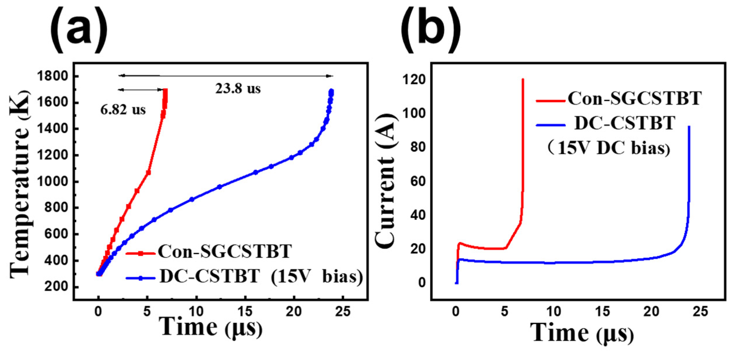
Figure 15 shows short-circuit waves. It indicates that the DC-CSTBT withstands a significantly longer short-circuit duration time (device failure time is defined when lattice temperature reaches 1687 K) than that of the C
on-SGCSTBT before failure. Owing to the smaller saturation current density, the short-circuit time of the proposed DC-CSTBT structure is about 2.48 times longer than that of the C
on-SGCSTBT.


