Article

Electrical Stability Modeling Based on Surface Potential for a-InGaZnO TFTs under Positive-Bias Stress and Light Illumination

1
College of Integrated Circuit Science and Engineering, Nanjing University of Posts and Telecommunications, Nanjing 210023, China
2
School of Communications and Information Engineering, Nanjing University of Posts and Telecommunications, Nanjing 210023, China
3
National Laboratory of Solid State Microstructures, Nanjing University, Nanjing 210093, China
*
Author to whom correspondence should be addressed.
Micromachines 2023, 14(4), 842; https://doi.org/10.3390/mi14040842
Submission received: 23 March 2023 / Revised: 8 April 2023 / Accepted: 11 April 2023 / Published: 13 April 2023
(This article belongs to the Special Issue Recent Advances in Thin Film Electronic Devices and Circuits)

Abstract

:
In this work, an electrical stability model based on surface potential is presented for amorphous In-Ga-Zn-O (a-IGZO) thin film transistors (TFTs) under positive-gate-bias stress (PBS) and light stress. In this model, the sub-gap density of states (DOSs) are depicted by exponential band tails and Gaussian deep states within the band gap of a-IGZO. Meanwhile, the surface potential solution is developed with the stretched exponential distribution relationship between the created defects and PBS time, and the Boltzmann distribution relationship between the generated traps and incident photon energy, respectively. The proposed model is verified using both the calculation results and experimental data of a-IGZO TFTs with various distribution of DOSs, and a consistent and accurate expression of the evolution of transfer curves is achieved under PBS and light illumination.

1. Introduction

Amorphous In-Ga-Zn-O (a-IGZO) thin film transistors (TFTs) have been widely investigated as pixel-switching and driving devices for active-matrix display technology because they offer high-current drive capacity, low off-state power consumption, and low-temperature uniform deposition compared with amorphous silicon-based TFTs [1,2]. However, there are high-density sub-gap defects located in the bandgap of a-IGZO, which cause a change in threshold voltage (ΔVth) and the degradation of subthreshold swing (ΔSS) under electrical and light stress, respectively [3,4]. Correspondingly, the uniformity of pixel-to-pixel brightness are affected in active-matrix display applications [5,6]. As a result, electrical stability modeling is required for the accurate stability prediction of a-IGZO TFTs under external stress conditions.
Up to now, some models for a-IGZO TFTs have been proposed to describe current–voltage characteristics, such as the surface potential ( φ s )-based compact model, charge-based capacitance model and unified dc/capacitance compact model [7,8,9]. Although the band-tail states and localized deep states are considered in these models for a-IGZO TFTs, the localized sub-gap density of states (DOSs) is invaluable in solving the model. Actually, new defects are generated in the device channel or at the a-IGZO/gate dielectric interface under external stress conditions [10,11]. For example, it has been demonstrated that the oxygen interstitial (Oi)-related defects are created in the device channel or the interface region under gate bias stress, originating from weakly bonded oxygen ions in a-IGZO TFTs [12,13]. Furthermore, the occupied deep-level oxygen vacancy (Vo) defects (energy width of ~1.5 eV) near the valence band maximum (VBM) in a-IGZO are ionized into single-ionized Vo (Vo+) and double-ionized Vo (Vo2+)-related defects under the corresponding incident photon energy [4,14]. In this work, to realize the electrical stability modeling for a-IGZO TFTs, the stretched exponential distribution relationship for created Oi-related defects as a function of the PBS time (t) and the Boltzmann distribution relation for generated Vo-related defects versus the incident photon energy (Eph) are adopted to calculate the φ s in the model. The accuracy of the proposed model is confirmed by comparison calculation results and the experimental data of a-IGZO TFTs with various fabrication conditions. It is found that the evolution of transfer curves for a-IGZO TFTs under PBS and light stress is in good agreement between the calculated and experimental results.
The back-gate structure of TFTs was applied for the modeling in this work, as shown in Figure 1. SiO2 (200 nm) thin film as a gate dielectric layer was grown on a heavily doped n-type Si substrate by plasma-enhanced chemical vapor deposition (PECVD) at a temperature of 300 °C. Next, a 50 nm a-IGZO film was deposited by pulsed laser deposition (PLD) at room temperature, and the oxygen partial pressure (Po2) was set at 1 Pa and 3 Pa, respectively. The composition of the ceramic target used was In:Ga:Zn = 2:2:1 in an atom ratio. The TFT channel region was then formed by optical photolithography and wet chemical etching. Subsequently, a Ti/Au bilayer was grown by e-beam evaporation for the source/drain metal electrode. The fabricated TFTs had a channel width and length of 200 µm and 40 µm, respectively. Finally, a SiO2 (100 nm) thin film used as a passivation layer was grown by PECVD. The samples were annealed in air at T = 300 °C.

2. Model Calculation

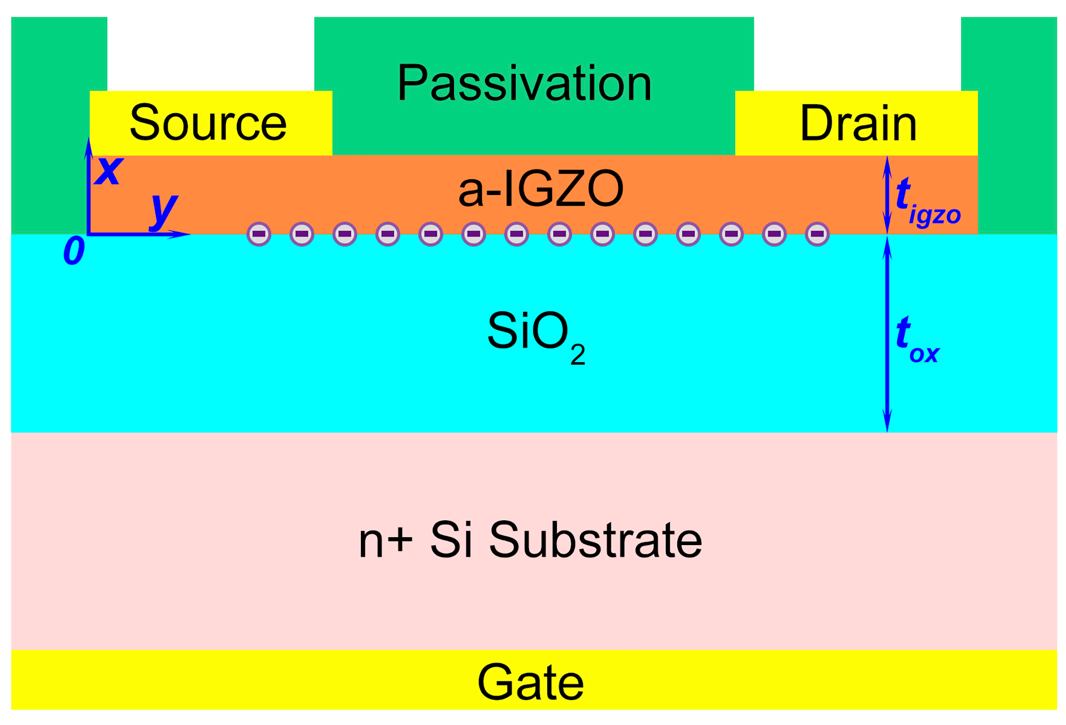
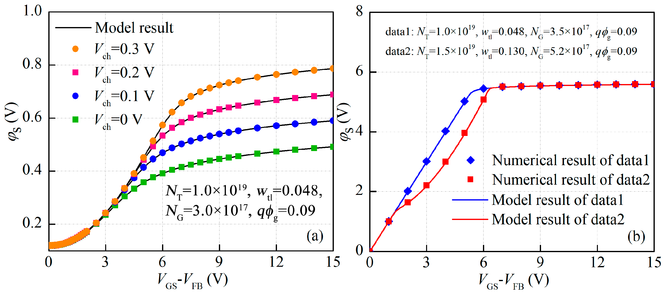
2.1. Surface Potential Model Calculation

For an n-type a-IGZO TFT, the sub-gap trap distribution comprises both the Gaussian deep states and exponential tails near the conduction band (EC) edge [15,16]. Based on the gradual channel approximation, the one-dimensional Poisson’s equation is given by
d 2 φ d x 2 = q ε igzo n free + n tail + n g
where the x-direction is defined as perpendicular to the channel direction, as shown in Figure 1. φ is the electrostatic potential, q is the electric charge, and ε igzo is the permittivity of a-IGZO. The free-electron concentration (nfree) in the channel, the electron concentration of tail states (ntail), and the electron concentration of deep states (ng) can be expressed as follows:
n free = n i exp E f + q φ V ch q ϕ f
n tail = N T exp E f E c + q φ V ch w tl ,
n g = k = 1 n d N k 1 + 1 g e E k E f q φ q ϕ f ,
where ni is the intrinsic electron concentration, ϕ f is the thermal voltage, Vch is the channel potential, and Ef is the Fermi-level energy; NT = gtail( π kT/sin( π kT/wtl)) when wtl > kT [17], herein, gtail is the tail states density at EC, and wtl is the conduction band tail slope. In this work, to solve the integration of Equation (4), the rectangle rule is applied to subdivide an integral interval into n equal rectangle levels [17]. In Equation (4), N k = N G exp E k E 0 2 / q ϕ g 2 , where NG is the peak value of the deep states, Ek is the center energy value of each discrete rectangle distribution, E0 is the energy value within the band gap corresponding to the peak of the deep states, q ϕ g is the characteristic decay energy of the deep states, d is the distance between every two discrete levels, and g is defined as the degenerescence constant. By combining Equation (1) with the derivative relation, 2 d φ / dx d 2 φ / d x 2 = d / dx d φ / dx 2 , the magnitude of the electric field (E( φ ) = d φ /dx) can be written as
d φ dx = 2 q ε igzo 0 φ n free + n tail + n g d φ .
By using Gauss’s law at the TFT interface region, the φ s can be expressed by
V GS V FB φ s = ε igzo E φ s C OX ,
where VGS is the gate-source voltage, VFB is the flat-band voltage, and COX is the oxide capacitance per unit area. Then, substituting Equation (5) into Equation (6), the relationship between the VGS and φ s can be written as
V GS V FB φ s = 2 q ε igzo N f exp φ s / ϕ f 1 + N tl exp q φ s / w tl 1 + N g 1 2 C OX ,
in the above Equation (7), N f = n free ϕ f exp φ / ϕ f , N tl = n tail ϕ tl exp q φ / w tl , and N g = ϕ f   k = 1 n N k ln C k + exp φ s / ϕ f . Herein, C k = 1 g ×   exp E k E f / q ϕ f .
Using charge-sheet approximation and then taking both the diffusion and drift current into account, the drain current can be expressed as
I DS y = μ E W ϕ f d Q i dy Q i d φ s dy ,
where μ E is the electron mobility, μ E = μ i V GS V FB p , μi and p are the fitting parameters, W is the channel width, y-direction is parallel to the device interface, and Qi is the induced charge density per unit area: Qi =COX(VGSVFB φ s ) − QtailQg. Herein, the charge density of the tail state (Qtail) and the charge density of the deep states (Qg) are given by
Q tail = 0 t igzo q n tail dx = q n igzo t igzo ,
Q g = 0 t igzo q n g dx = q n g t igzo ,
and consequently, Equation (8) can be obtained by integrating this along the y-direction. The result can be expressed as
I DS = μ E W L ϕ f Q i φ sd Q i φ ss φ ss φ sd Q i φ s d φ s
where L is the channel length, and φ sd and φ ss are the value of φ s when Vch = VDS and Vch = 0 V, respectively. In Equation (11), the integral result of Qi( φ s ) can be written as
G ( φ s ) = q t igzo [ ϕ tail n tail + ϕ f k = 1   n N k ln ( C k + e φ s ϕ f ) ]
Finally, substituting Equation (12) with Equation (11), the drain current (IDS) equation can be obtained as
I DS = μ E W L ϕ f Q i φ sd Q i φ ss G φ sd G φ ss .

2.2. Model Verification

To confirm the accuracy of the model, the φ s solution is compared with numerical results with different Vch values and defect distributions.
As shown in Figure 2a,b, it was found that the surface potential characteristics are in line with numerical results. The parameters for the model calculation are summarized in Table 1. Meanwhile, to further evaluate the model validity, a comparison of the model results with the measured experimental data from a-IGZO TFTs fabricated with Po2 values of 1 Pa and 3 Pa was carried out. It has been demonstrated that DOSs mainly originate from Vo-related traps in a-IGZO, and the distribution of DOSs is affected by the Po2 during channel layer deposition [18,19]. Correspondingly, the quantity of Vo within the a-IGZO films grown with Po2 values of 1 Pa and 3 Pa was analyzed by X-ray photoelectron spectroscopy (XPS). As shown in Figure 3a,b, the binding energy peaks at 530.1 eV, 530.9 eV, and 532 eV are associated with the O2 ions combined with metal atoms (M-O), Vo, and OH, respectively [20,21]. The relative amount of Vo in the a-IGZO films could be described by the area ratio of the Vo peak to the total O 1s peak, which are 37% and 32% for a-IGZO films grown with Po2 values of 1 Pa and 3 Pa, respectively. Therefore, the output and transfer characteristics of devices fabricated with Po2 values of 1 Pa and 3 Pa are used to compare with those of the model. As shown in Figure 4a,b, the model results are in accordance with the measured I–V curves for a-IGZO TFTs. The obtained model parameters are presented in Table 1. Thus, these results confirm that the model can accurately predict the I–V characteristics for a-IGZO TFTs with various distributions of DOSs. In addition, it has been reported that new trap states are generated for a-IGZO TFTs under PBS and light stress, which cause the diminishment in electrical performance [10,22,23]. Therefore, in the following, the newly created defect DOS model is used to describe the electrical stability of a-IGZO TFTs under external stress conditions.

3. Results and Discussions

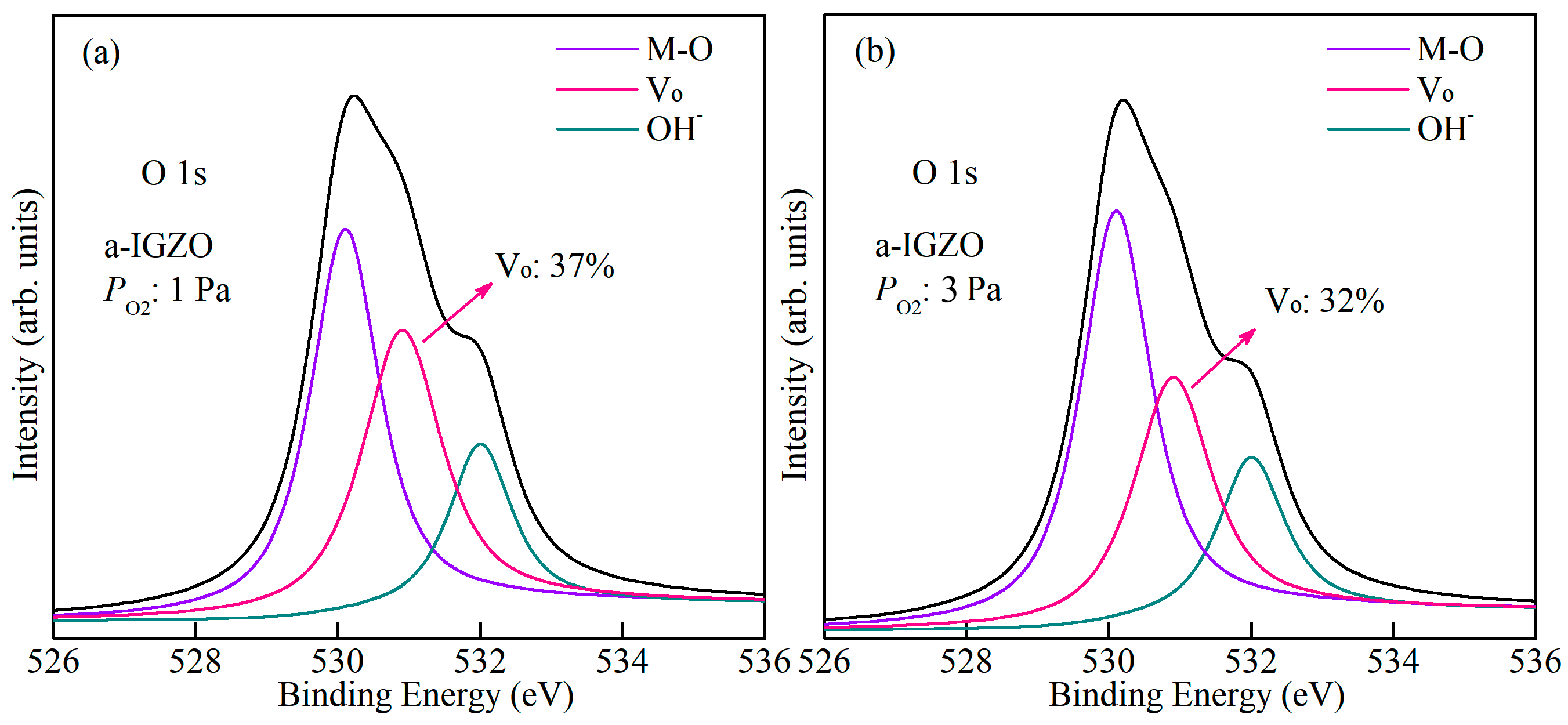
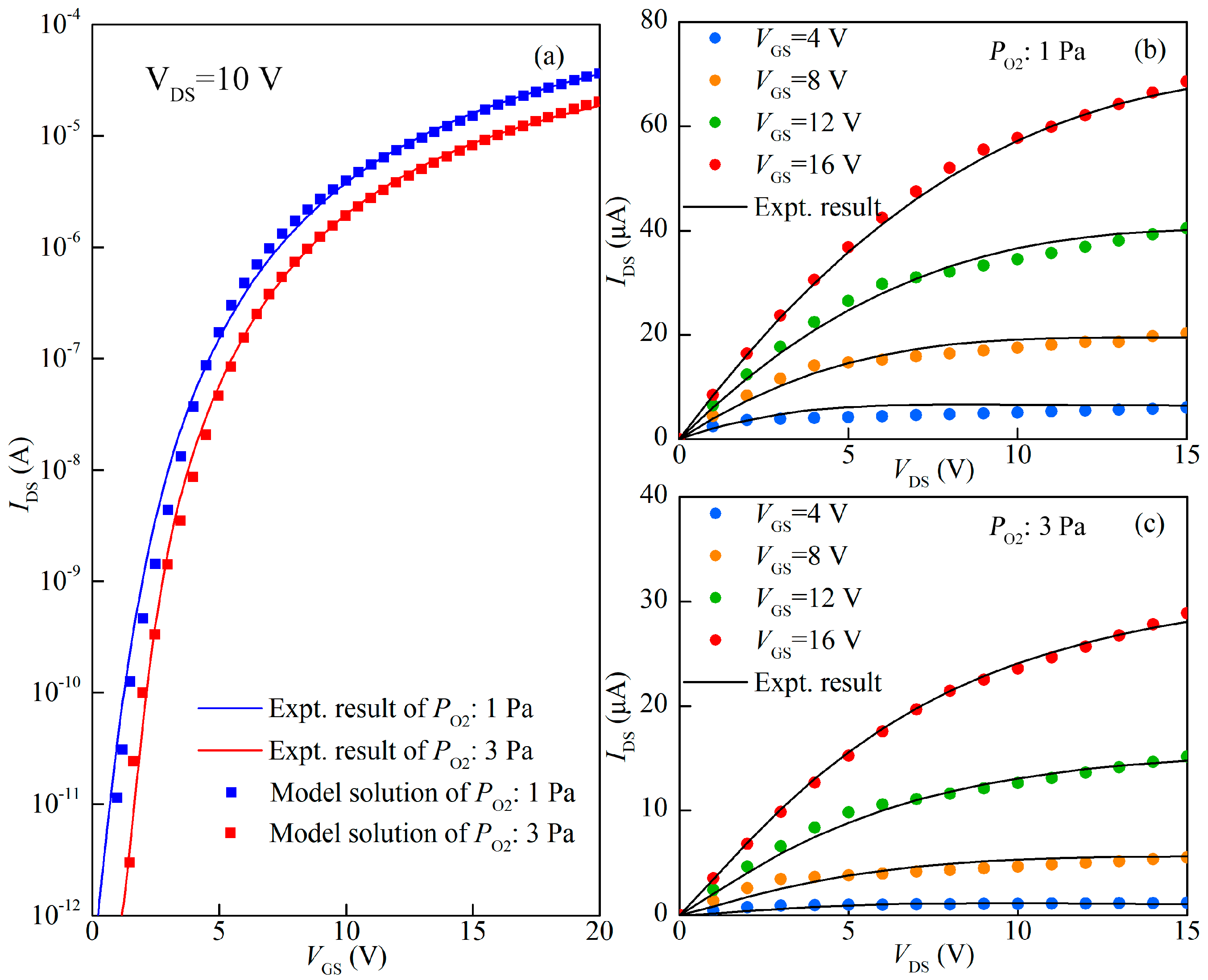
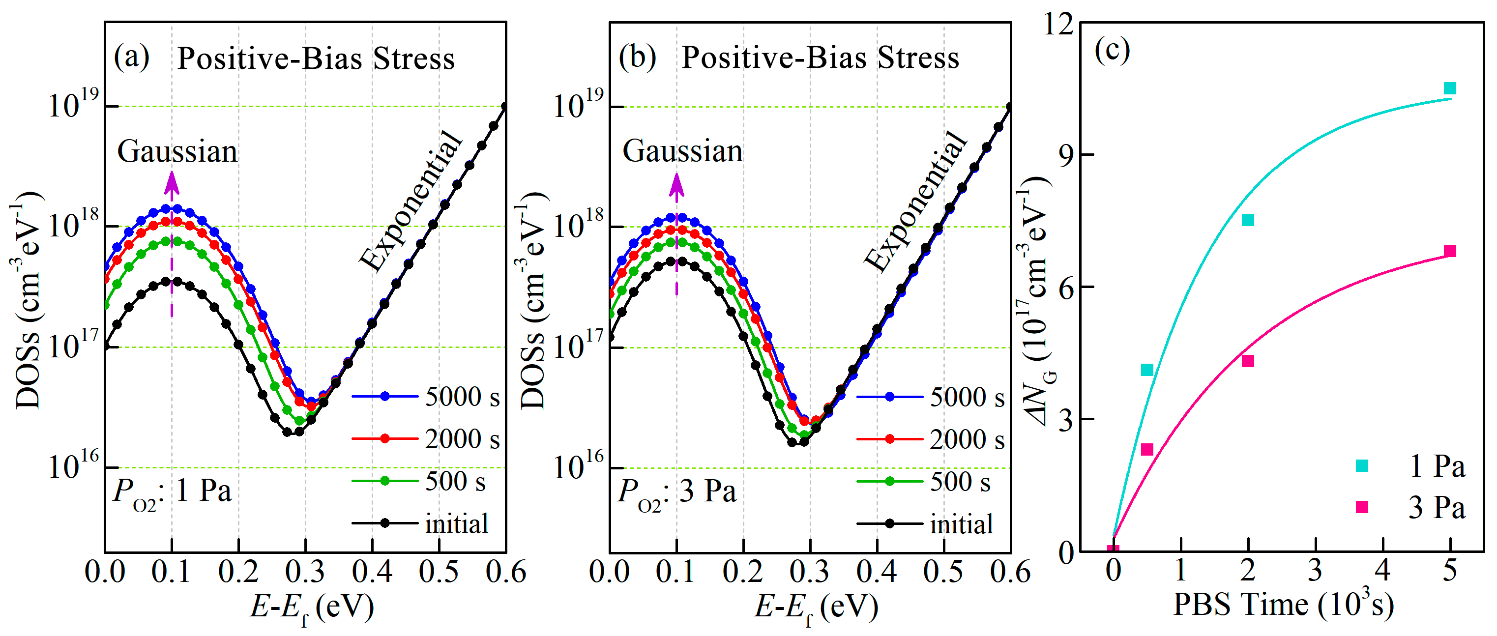
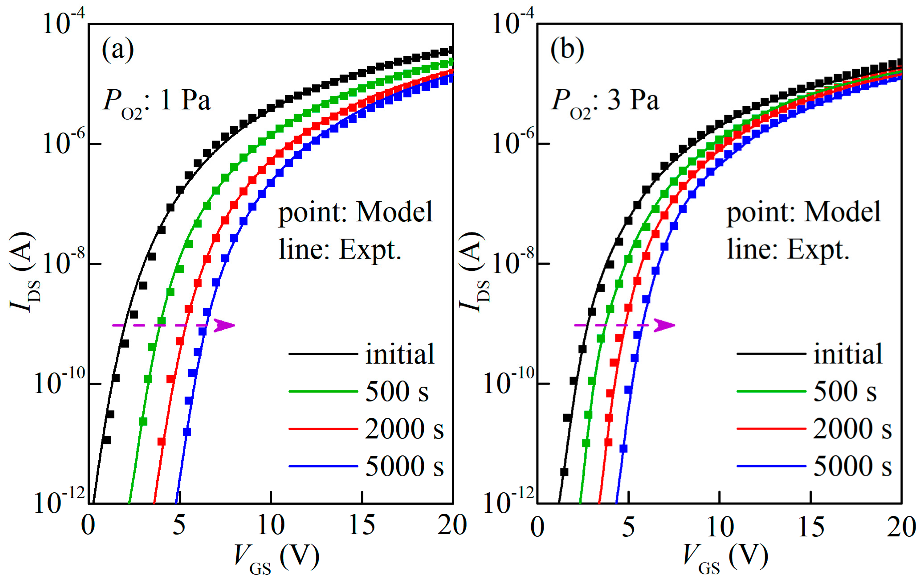
3.1. The Model of a-IGZO TFTs under PBS

It has been demonstrated that the ΔVth values for a-IGZO TFTs under PBS are mainly ascribed to the creation of oxygen-related traps [10,24]. Under PBS, the oxygen interstitials (Oi) are generated from the weakly bonded oxygen ions in a-IGZO, which are in an octahedral configuration [Oi(oct)] and are electrically active. The created Oi(oct)-related defects located above the mid-gap are occupied by trapping electrons and become the negatively charged defect [Oi2(oct)] when the Ef increases under PBS, which causes a positive drift in the transfer curve of a-IGZO TFTs [24,25]. Meanwhile, the generated Oi2(oct)-related defects are transformed into deep-level negative-U states due to the structural relaxation effect. Because the generated Oi(oct)-related defects are distributed above the mid-gap, the peak value of the Gaussian-distributed deep defects are adjusted to describe the generation of new defects of a-IGZO TFTs during the PBS process. In previous reports, the ΔVth in a-IGZO TFTs under PBS depended on the characteristic trapping time of carriers (τ) and the dispersion parameter of the barrier energy height (β), which is in accordance with the stretched exponential distribution relationship [26,27]. Therefore, in this work, the amount of created Oi-related traps (ΔNG) with the increase of PBS time (t) can be expressed as follow:
Δ N G = α V 0 { 1 exp [ ( t τ ) β ] }
where α is the fitting parameter relating to the DOSs, and V0 is Vbias-Vth0 (Vbias and Vth0 are the PBS voltage and the initial Vth of the device, respectively).
Next, substituting Equation (14) into Equation (3), the modified DOSs model can be written as
N k = N G + Δ N G exp E k E 0 q ϕ g 2 .
Finally, the IDS of a-IGZO TFTs under PBS could be calculated by using the proposed DOSs model.
To validate the proposed scheme, the model is compared with the experimental results from the evolution of transfer curves versus PBS time for devices fabricated with Po2 values of 1 Pa and 3 Pa, respectively. The PBS stability of the a-IGZO TFTs is measured at a VGS of 20 V for the PBS time of 5000 s. Based on the proposed DOS model calculation, it is clear that the peak value of the Gaussian-distributed oxygen-related defects (NG) is increased as the PBS time increases for the a-IGZO TFTs, as shown in Figure 5a,b. Meanwhile, the ΔNG after 5000 s of PBS is 1.05 × 1018 cm−3eV−1 and 6.8 × 1017 cm−3eV−1 for a-IGZO TFTs with Po2 values of 1 Pa and 3 Pa, respectively. In addition, as shown in Figure 6a,b, it is found that the evolution of transfer curves for the devices calculated using the defect DOS model agrees well with the experimental results, and the specific values of the relevant parameters are listed in Table 2. Correspondingly, the ΔVth values are 4.5 V and 2.5 V for a-IGZO TFTs fabricated with Po2 values of 1 Pa and 3 Pa, suggesting that the oxygen-related defects are suppressed in the channel by the increasing in Po2. This result can also be supported by XPS analysis. Thus, the presented results confirm that the model could accurately predict the PBS stability of a-IGZO TFTs.

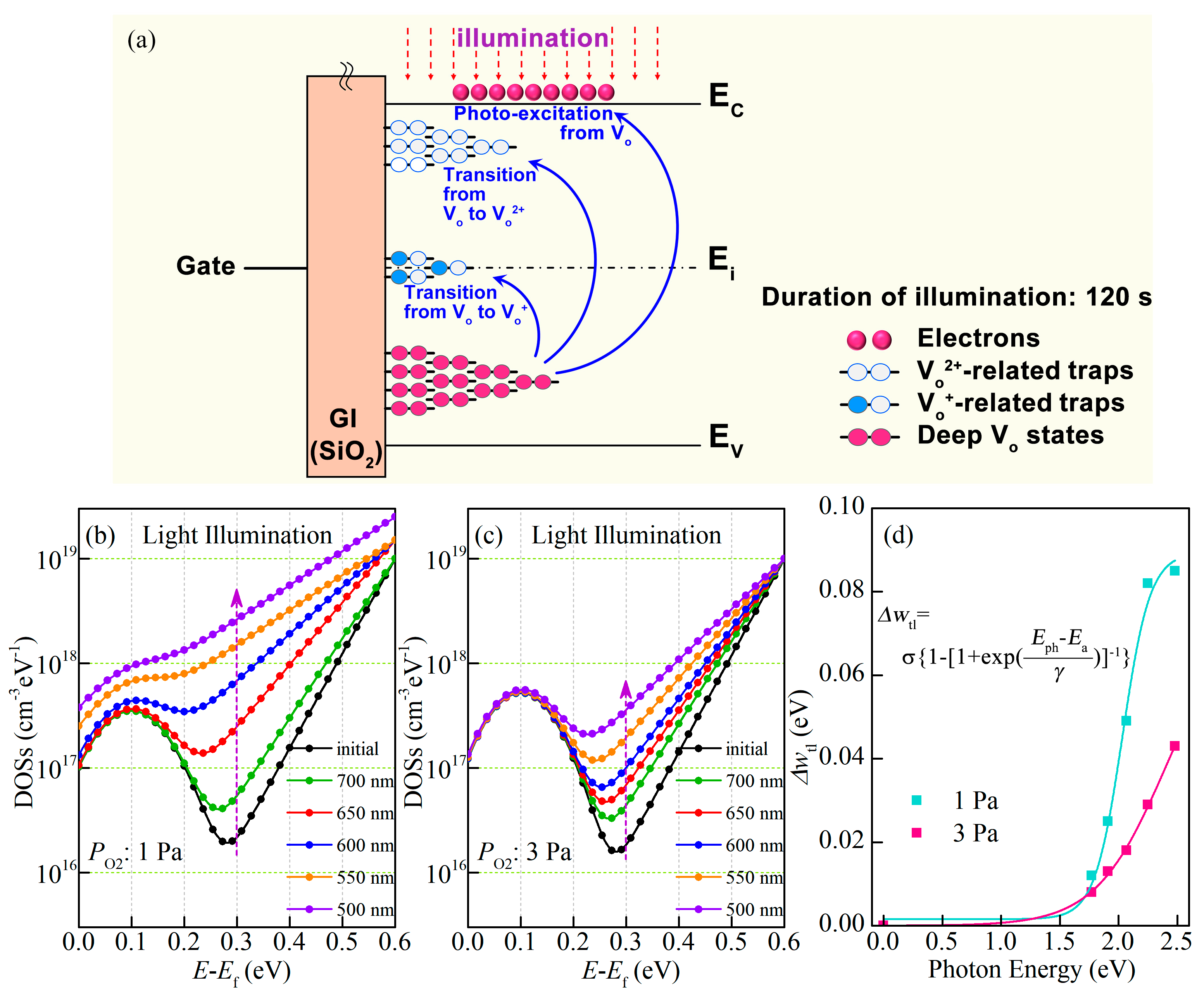
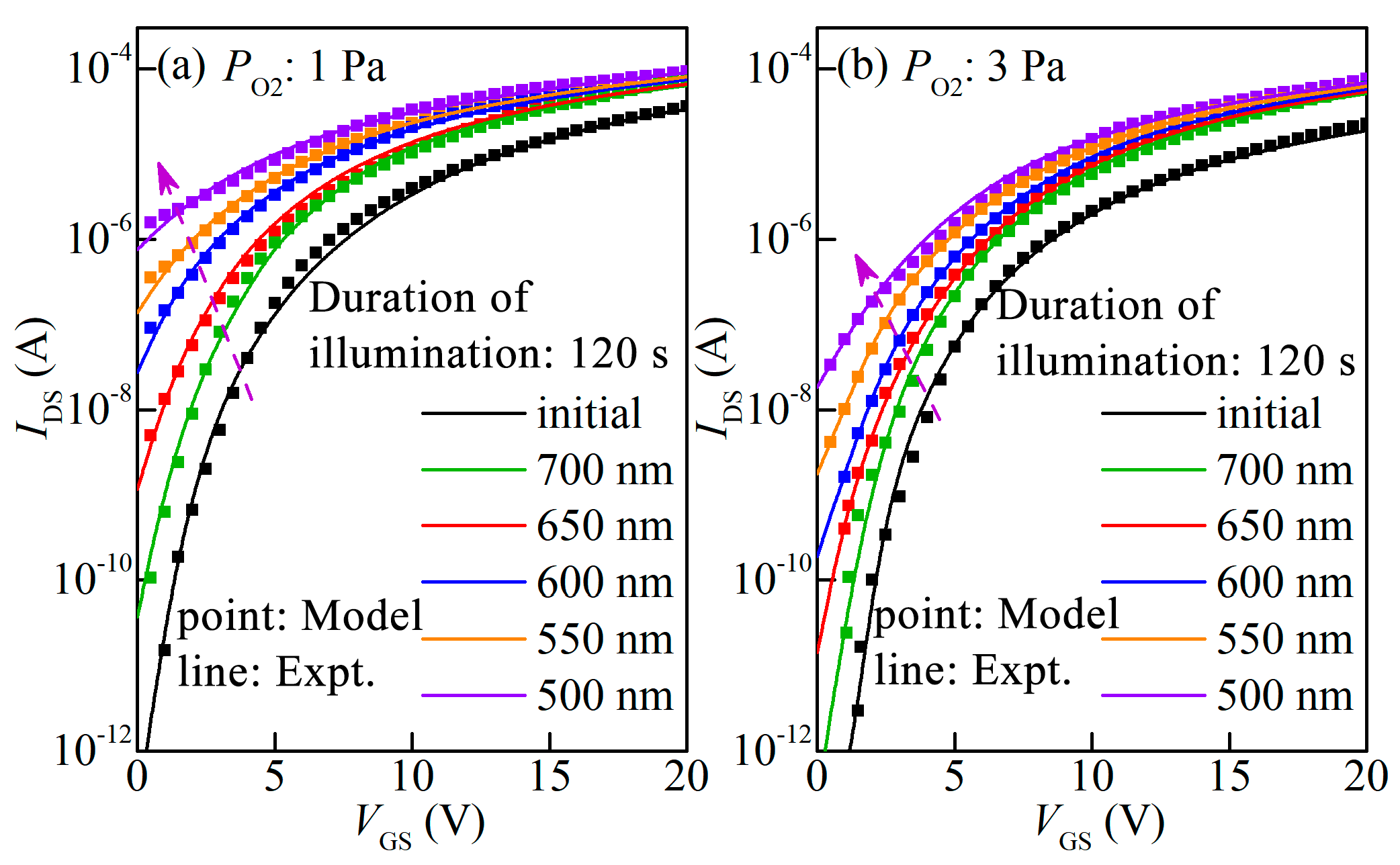
3.2. The Model of a-IGZO TFTs under Light Illumination

It has been demonstrated that there are high-density entirely occupied Vo values existing in the VBM with the energy distribution of ~1.5 eV, which are ionized to Vo+ and Vo2+ under short-wavelength light. During photo-excited ionization processes, the new unoccupied defect states are generated at the bottom of EC and mid-gap due to the outward lattice relaxation effect [28,29]. Meanwhile, the values of the activation energy (Ea) for the photo-induced transition from Vo to Vo+ and Vo2+ are ~2.0 eV and ~2.3 eV, respectively. Figure 7a shows the process of generating Vo-related traps in a-IGZO under monochromatic light. Since the generated Vo-related defects are mainly distributed near the bottom of the EC [29,30], the conduction band tail slope is adjusted to describe the creation of Vo-related defects for a-IGZO TFTs under a light illumination process. It has been reported that the exponential band tails can be expressed by a generalization of Boltzmann relations in semiconductor materials [31,32]. Thus, in this work, the Boltzmann distribution relation is applied to describe the generated Vo-related defects at the bottom of the EC under light conditions. The amount of change in the conduction band tail slope (Δwtl) versus the incident photon energy (Eph) can be written as
Δ w tl = σ { 1 [ 1 + exp ( E ph E a γ ) ] 1 }
where σ is the fitting parameter, and γ is the fitting parameter in proportion to the oxygen partial pressure. Substituting Equation (16) with Equation (4), the density of the tail state (NTL) model of a-IGZO TFTs under light stress can be given by
N TL = g tail exp E E c w tl + Δ w tl .
As a result, the IDS of a-IGZO TFTs under light conditions could be calculated by using the proposed DOS model. To check the proposed scheme, a comparison between the model and the measured transfer curves of a-IGZO TFTs under monochromatic light at various wavelengths for 120 s was carried out. According to the proposed DOS model calculation, it is clear that the Δwtl is increased as the wavelength of incident light is reduced from 700 nm to 500 nm for the a-IGZO TFTs, as shown in Figure 7b,c. Correspondingly, the Δwtl values are 0.085 eV and 0.043 eV for a-IGZO TFTs with Po2 values of 1 Pa and 3 Pa after λ = 500 nm, as shown in Figure 7d. Meanwhile, the evolution of transfer curves for a-IGZO TFTs calculated using the proposed DOS model is in good accordance with the experimental results, as shown in Figure 8a,b. The specific values of the relevant parameters are listed in Table 3. Under light illumination, the transfer curves of TFTs drift toward the negative direction as the incident wavelength light reduces from 700 nm to 500 nm, which are induced by the photo-excited electrons from the occupied interface defects and occupied deep Vo states. In addition, it has been demonstrated that the ΔSS is associated with the amount of created defects (ΔNt) within the device’s active region [33,34]. It is found that the ΔSS values for devices fabricated with Po2 values of 1 Pa and 3 Pa are 0.9 V/dec and 0.5 V/dec after λ = 500 nm, suggesting that deep-level Vo can be suppressed by increasing Po2. Therefore, these results demonstrate that the model could accurately predict the light stability of a-IGZO TFTs.

4. Conclusions

In this work, an electrical stability model based on surface potential for a-IGZO TFTs considering both exponential band tails and Gaussian deep states has been proposed. In this model, a reasonable method is presented for solving the surface potential by using the stretched exponential and Boltzmann distribution relation to describe the generated defects as a function of external stress conditions, the feasibility of which has been demonstrated by achieving good agreement between calculation results and experimental data of a-IGZO TFTs under PBS and light conditions. Thus, the proposed model is accurate and useful for predicting the electrical stability of a-IGZO TFTs.

Author Contributions

Conceptualization, X.H., W.C., C.H. and C.C.; writing—original draft preparation, W.C.; writing—review and editing, X.H., C.H., Z.S. and W.X. All authors have read and agreed to the published version of the manuscript.

Funding

This research was funded by the National Natural Science Foundation of China (grant no. 61904086 and 62274096) and China Postdoctoral Science Foundation (grant no. SBH19006).

Data Availability Statement

The data presented in this study are available on request from the corresponding author.

Conflicts of Interest

The funders had no role in the design of the study; in the collection, analyses, or interpretation of data; in the writing of the manuscript; or in the decision to publish the results.

References

  1. Nomura, K.; Ohta, H.; Takagi, A.; Kamiya, T.; Hirano, M.; Hosono, H. Room-temperature fabrication of transparent flexible thin-film transistors using amorphous oxide semiconductors. Nature 2004, 432, 488–492. [Google Scholar] [CrossRef] [PubMed]
  2. Cho, M.H.; Seol, H.; Yang, H.; Yun, P.S.; Bae, J.U.; Park, K.-S.; Jeong, J.K. High-performance amorphous indium gallium zinc oxide thin-film transistors fabricated by atomic layer deposition. IEEE Electron Device Lett. 2018, 39, 688–691. [Google Scholar] [CrossRef]
  3. Kim, J.; Kim, H.; Oh, J.; Choi, S.-Y.; Park, H. Turn-around of threshold voltage shift in amorphous InGaZnO TFT under positive bias illumination stress. Solid-State Electron. 2023, 201, 108605. [Google Scholar] [CrossRef]
  4. Kim, W.; Lee, W.J.; Kwak, T.; Baek, S.; Lee, S.H.; Park, S. Influence of UV/ozone treatment on threshold voltage modulation in sol–gel IGZO thin-film transistors. Adv. Mater. Interfaces 2022, 9, 2200032. [Google Scholar] [CrossRef]
  5. Jeong, J. The status and perspectives of metal oxide thin-film transistors for active matrix flexible displays. Semicond. Sci. Technol. 2011, 26, 034008. [Google Scholar] [CrossRef]
  6. Bagheri, M.; Cheng, X.; Zhang, J.; Lee, S.; Ashtiani, S.; Nathan, A. Threshold voltage compensation error in voltage programmed AMOLED displays. J. Disp. Technol. 2016, 12, 658–664. [Google Scholar] [CrossRef] [Green Version]
  7. Zong, Z.; Li, L.; Jang, J.; Lu, N.; Liu, M. Analytical surface-potential compact model for amorphous-IGZO thin-film transistors. J. Appl. Phys. 2015, 117, 215705. [Google Scholar] [CrossRef]
  8. Moldovan, O.; Castro-Carranza, A.; Estrada, M.; Cerdeira, A.; Lime, F.; Iniguez, B. A complete charge-based capacitance model for IGZO TFTs. IEEE Electron Device Lett. 2019, 40, 730–733. [Google Scholar] [CrossRef]
  9. Deng, W.; Fang, J.; Wei, X.; Wu, W.; Huang, J. A core compact model for IGZO TFTS considering degeneration mechanism. IEEE Trans. Electron Devices 2018, 65, 1370–1376. [Google Scholar] [CrossRef]
  10. Chowdhury, M.; Migliorato, P.; Jang, J. Time-temperature dependence of positive gate bias stress and recovery in amorphous indium-gallium-zinc-oxide thin-film-transistors. Appl. Phys. Lett. 2011, 98, 153511. [Google Scholar] [CrossRef]
  11. Hung, M.; Wang, D.; Furuta, M. Investigating effect of postannealing time on positive bias stress stability of In–Ga–Zn–O TFT by conductance method. IEEE Trans. Electron Devices 2015, 62, 3697–3702. [Google Scholar] [CrossRef]
  12. Zhou, X.; Shao, Y.; Zhang, L.; Lu, H.; He, H.; Han, D.; Wang, Y.; Zhang, S. Oxygen interstitial creation in a-IGZO thin-film transistors under positive gate-bias stress. IEEE Electron Device Lett. 2017, 38, 1252–1255. [Google Scholar] [CrossRef]
  13. Lee, E.; Park, J.; Lee, S.; Na, H.; Cho, N.; Im, C.; Cho, Y.; Kim, Y. Oxygen radical control via atmospheric pressure plasma treatment for highly stable IGZO thin-film transistors. IEEE Trans. Electron Devices 2020, 67, 3135–3140. [Google Scholar] [CrossRef]
  14. Kuk, S.; Lee, S.; Kim, S.; Kim, B.; Park, S.; Kwon, J.; Han, M. Light-induced hysteresis of In–Ga–Zn–O thin-film transistors with various temperatures. IEEE Electron Device Lett. 2012, 33, 1279–1281. [Google Scholar] [CrossRef]
  15. Tsormpatzoglou, A.; Hastas, N.; Choi, N.; Mahmoudabadi, F.; Hatalis, M.; Dimitriadis, C. Analytical surface-potential-based drain current model for amorphous InGaZnO thin film transistors. J. Appl. Phys. 2013, 114, 184502. [Google Scholar] [CrossRef]
  16. Jang, J.; Ko, D.; Choi, S.; Kim, D.; Kim, D. Observation of hydrogen-related defect in subgap density of states and its effects under positive bias stress in amorphous InGaZnO TFT. IEEE Electron Device Lett. 2021, 42, 708–711. [Google Scholar] [CrossRef]
  17. Deng, W.; Huang, J.; Li, X. Surface-potential-based drain current model of polysilicon TFTs with gaussian and exponential DOS distribution. IEEE Trans. Electron Devices 2011, 59, 94–100. [Google Scholar] [CrossRef]
  18. Yang, G.; Park, J.; Choi, S.; Kim, C.; Kim, D.M.; Choi, S.; Bae, J.; Cho, I.; Kim, D. Total subgap range density of states-based analysis of the effect of oxygen flow rate on the bias stress instabilities in a-IGZO TFTs. IEEE Trans. Electron Devices 2022, 69, 166–173. [Google Scholar] [CrossRef]
  19. Oka, N.; Aoi, T.; Hayashi, R.; Kumomi, H.; Shigesato, Y. Electronic state of amorphous indium gallium zinc oxide films deposited by dc magnetron sputtering with water vapor introduction. Appl. Phys. Express 2012, 5, 075802. [Google Scholar] [CrossRef]
  20. Yang, S.; Ji, K.; Kim, U.; Hwang, C.; Park, S.; Hwang, C.; Jang, J.; Jeong, J. Suppression in the negative bias illumination instability of Zn-Sn-O transistor using oxygen plasma treatment. Appl. Phys. Lett. 2011, 99, 102103. [Google Scholar] [CrossRef]
  21. Nomura, K.; Kamiya, T.; Ikenaga, E.; Yanagi, H.; Kobayashi, K.; Hosono, H. Depth analysis of subgap electronic states in amorphous oxide semiconductor, a-In-Ga-Zn-O, studied by hard X-ray photoelectron spectroscopy. J. Appl. Phys. 2011, 109, 073726. [Google Scholar] [CrossRef]
  22. Ha, T.; Kim, Y.; Cho, Y.; Kang, Y.; Yu, S.; Kim, G.; Jeong, H.; Park, J.; Kim, O. Defect-creation effects on abnormal on-current under drain bias illumination stress in a-IGZO thin-film transistors. Solid-State Electron. 2020, 165, 107752. [Google Scholar] [CrossRef]
  23. Um, J.; Mativenga, M.; Migliorato, P.; Jang, J. Increase of interface and bulk density of states in amorphous-indium-gallium-zinc-oxide thin-film transistors with negative-bias-under-illumination-stress time. Appl. Phys. Lett. 2012, 101, 113504. [Google Scholar]
  24. Nomura, K.; Kamiya, T.; Hirano, M.; Hosono, H. Origins of threshold voltage shifts in room-temperature deposited and annealed a-In–Ga–Zn–O thin-film transistors. Appl. Phys. Lett. 2009, 95, 013502. [Google Scholar] [CrossRef]
  25. Choi, S.; Choi, S.J.; Kim, D.; Park, S.; Kim, J.; Seo, Y.; Shin, H.; Jeong, Y.; Bae, J.; Oh, C.; et al. Positive bias stress instability of InGaZnO TFTs with self-aligned top-gate structure in the threshold-voltage compensated pixel. IEEE Electron Device Lett. 2020, 41, 50–53. [Google Scholar] [CrossRef]
  26. Hsu, S.; He, J.; Li, Y.; Su, D.; Tsai, F.; Cheng, I. Effect of mechanical strain on electrical performance of flexible p-type SnO thin-film transistors. IEEE Trans. Electron Devices 2019, 66, 5183–5186. [Google Scholar] [CrossRef]
  27. Costa, J.; Kermani, A.; Cantarella, G.; Petti, L.; Vogt, C.; Daus, A.; Knobelspies, S.; Troster, G.; Munzenrieder, N. Long-term aging of Al2O3 passivated and unpassivated flexible a-IGZO TFTs. IEEE Trans. Electron Devices 2020, 67, 4934–4939. [Google Scholar] [CrossRef]
  28. Huang, X.; Wu, C.; Lu, H.; Ren, F.; Xu, Q.; Ou, H.; Zhang, R.; Zheng, Y. Electrical instability of amorphous indium-gallium-zinc oxide thin film transistors under monochromatic light illumination. Appl. Phys. Lett. 2012, 100, 243505. [Google Scholar] [CrossRef] [Green Version]
  29. Billah, M.; Chowdhury, M.; Mativenga, M.; Um, J.; Mruthyunjaya, R.; Heiler, G.; Tredwell, T.; Jang, J. Analysis of improved performance under negative bias illumination stress of dual gate driving a-IGZO TFT by TCAD simulation. IEEE Electron Device Lett. 2016, 37, 735–737. [Google Scholar] [CrossRef]
  30. Kim, Y.; Kim, S.; Kim, W.; Bae, M.; Jeong, H.; Kong, D.; Choi, S.; Kim, D.; Kim, D.H. Amorphous InGaZnO thin-film transistors—Part II: Modeling and simulation of negative bias illumination stress-induced instability. IEEE Trans. Electron Devices 2012, 59, 2699–2706. [Google Scholar] [CrossRef]
  31. Tsurumi, J.; Matsui, H.; Kubo, T.; Häusermann, R.; Mitsui, C.; Okamoto, T.; Watanabe, S.; Takeya, J. Coexistence of ultra-long spin relaxation time and coherent charge transport in organic single-crystal semiconductors. Nat. Phys. 2017, 13, 994–998. [Google Scholar] [CrossRef]
  32. Beckers, A.; Beckers, D.; Jazaeri, F.; Parvais, B.; Enz, C. Generalized boltzmann relations in semiconductors including band tails. J. Appl. Phys. 2021, 129, 045701. [Google Scholar] [CrossRef]
  33. Xie, H.; Wu, Q.; Xu, L.; Zhang, L.; Liu, G.; Dong, C. Nitrogen-doped amorphous oxide semiconductor thin film transistors with double-stacked channel layers. Appl. Surf. Sci. 2016, 387, 237–243. [Google Scholar] [CrossRef]
  34. Yang, Z.; Meng, T.; Zhang, Q.; Shieh, H. Stability of amorphous indium–tungsten oxide thin-film transistors under various wavelength light illumination. IEEE Electron Device Lett. 2016, 37, 437–440. [Google Scholar] [CrossRef]
Figure 1. Schematic diagram of a-IGZO TFTs used in modeling.
Micromachines 14 00842 g001
Figure 2. Comparison of the surface potential solution with the numerical result for (a) different values of Vch and (b) various DOS distributions.
Micromachines 14 00842 g002
Figure 3. O 1s XPS spectra of a-IGZO thin films fabricated with Po2 values of (a) 1 Pa and (b) 3 Pa.
Micromachines 14 00842 g003
Figure 4. Comparison of (a) transfer characteristics and (b,c) output characteristics for a-IGZO TFTs fabricated with Po2 values of 1 Pa and 3 Pa between the model results and experimental data.
Micromachines 14 00842 g004
Figure 5. Calculated DOSs as a function of PBS time for a-IGZO TFTs fabricated with different Po2 values: (a) 1 Pa and (b) 3 Pa; (c) the shift of NG for a-IGZO TFTs fabricated with Po2 values of 1 Pa and 3 Pa.
Micromachines 14 00842 g005
Figure 6. Measured evolution of the transfer curves as a function of PBS time for a-IGZO TFTs fabricated with different Po2 values compared with model results: (a) 1 Pa and (b) 3 Pa.
Micromachines 14 00842 g006
Figure 7. (a) Schematic diagram of the Vo-related defect generation process for a-IGZO TFTs under short-wavelength light. Calculated DOSs as a function of monochromatic light illumination for a-IGZO TFTs fabricated with different Po2 values: (b) 1 Pa and (c) 3 Pa; (d) the shift of wtl for a-IGZO TFTs fabricated with Po2 values of 1 Pa and 3 Pa.
Micromachines 14 00842 g007
Figure 8. Measured evolution of transfer curves as a function of various conditions of monochromatic light illumination for a-IGZO TFTs fabricated with different Po2 values compared with model results: (a) 1 Pa and (b) 3 Pa.
Micromachines 14 00842 g008
Table 1. Key parameters used in the model.
ParametersValueUnitParametersValueUnit
q1.6 × 10−19Cd0.05eV
εigzo11.5-E02.7eV
COX1.73 × 10−4F/m2μi5cm2s−1/V1+p
VFB0Vp0.7-
VDS10VW200µm
ϕf0.026VL40µm
Ef2.6eVtigzo50nm
Table 2. Parameters of the DOSs under PBS.
ParameterPo2 [Pa]InitialPBS Time [s]
50020005000
NT [cm−3eV−1]11 × 10191 × 10191 × 10191 × 1019
31 × 10191 × 10191 × 10191 × 1019
wtl [eV]10.0480.0480.0480.048
30.0470.0470.0470.045
NG [cm−3eV−1]13.5 × 10177.6 × 10171.1 × 10181.4 × 1018
35.2 × 10177.5 × 10179.5 × 10171.2 × 1018
g [eV]10.090.090.0950.095
30.0830.0850.090.09
β10.85
3
τ[s]11544.58
31902.39
α16.43 × 10¹⁶
35.49 × 10¹⁶
Table 3. Parameters of the DOSs under illumination.
ParameterPo2 [Pa]InitialWavelength of Light [nm]
750650600550500
NT [cm−3eV−1]11 × 10191 × 10191.5 × 10191.5 × 10191.5 × 10192.5 × 1019
31 × 10191 × 10191 × 10191 × 10191 × 10191 × 1019
wtl [eV]10.0480.0600.0730.0970.1300.133
30.0470.0550.0600.0650.0760.090
NG [cm−3eV−1]13.5 × 10173.5 × 10173.5 × 10173.5 × 10173.5 × 10173.5 × 1017
35.2 × 10175.2 × 10175.2 × 10175.2 × 10175.2 × 10175.2 × 1017
g [eV]10.090.090.090.090.090.09
30.0830.0830.0830.0830.0830.083
Ea [eV]12.3
3
γ10.1
30.3
σ10.089
30.076
Disclaimer/Publisher’s Note: The statements, opinions and data contained in all publications are solely those of the individual author(s) and contributor(s) and not of MDPI and/or the editor(s). MDPI and/or the editor(s) disclaim responsibility for any injury to people or property resulting from any ideas, methods, instructions or products referred to in the content.

