
Vertical GaN MOSFET Power Devices
 and
and 
Abstract
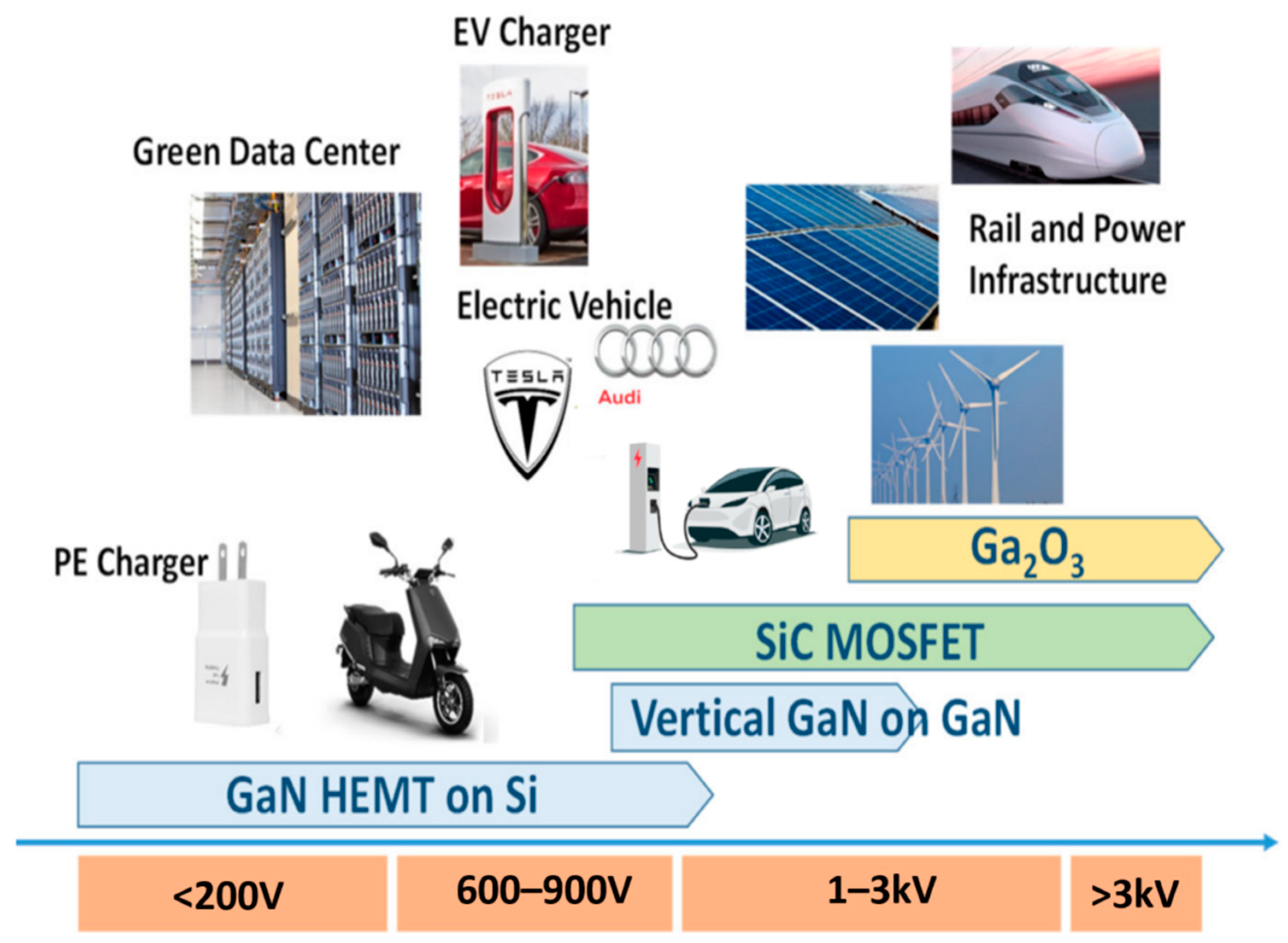
:1. Introduction
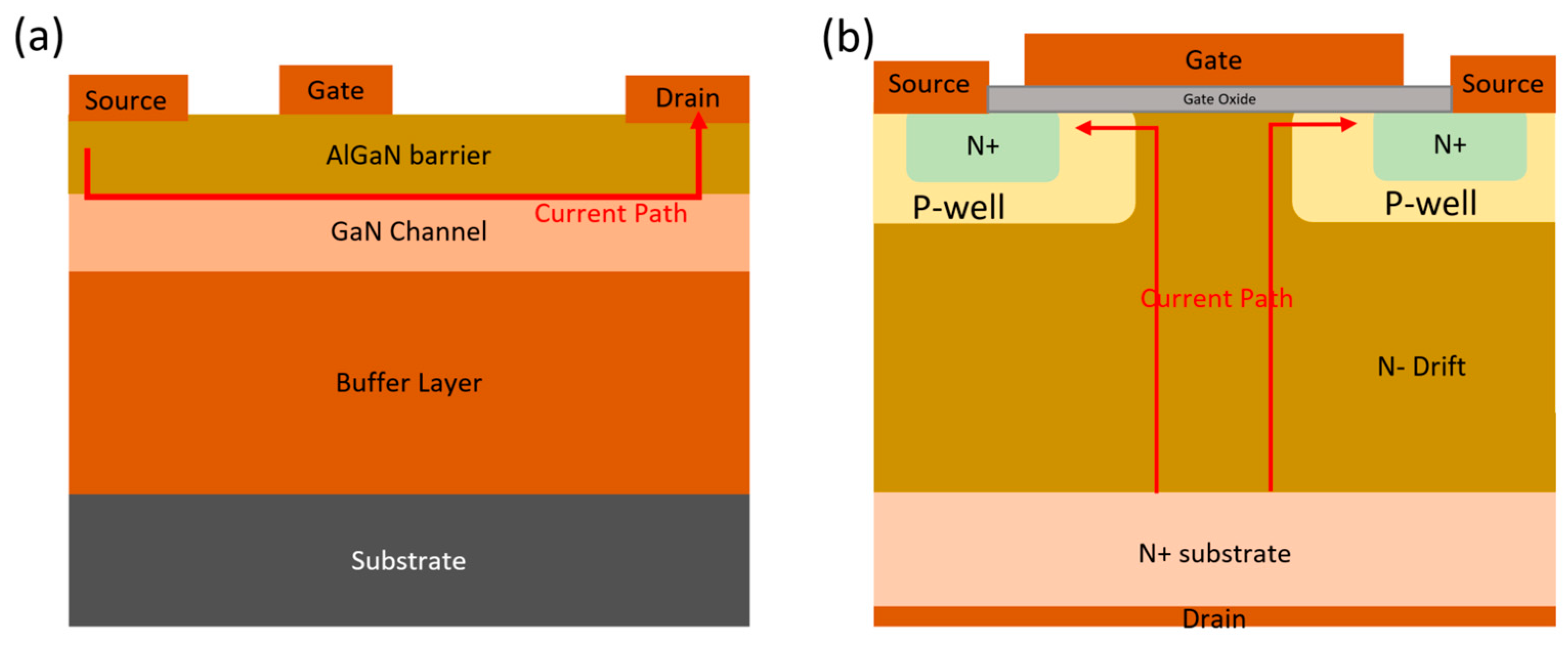
2. GaN Power Devices
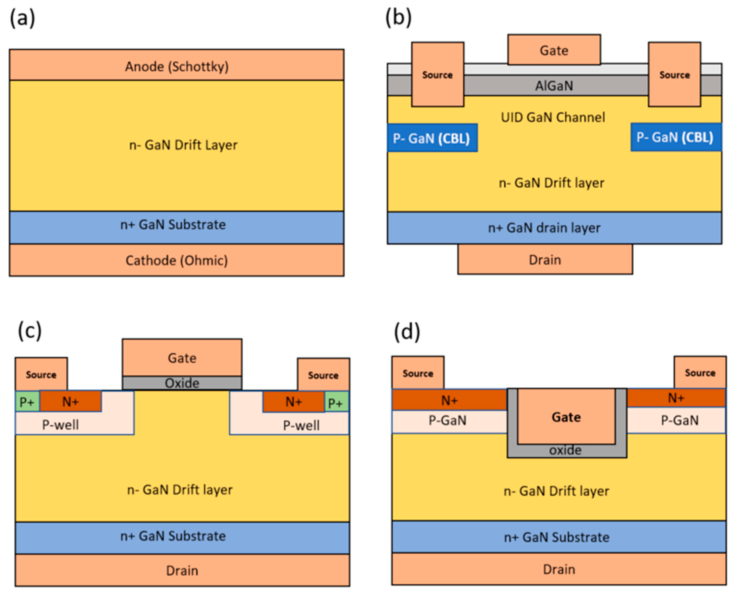
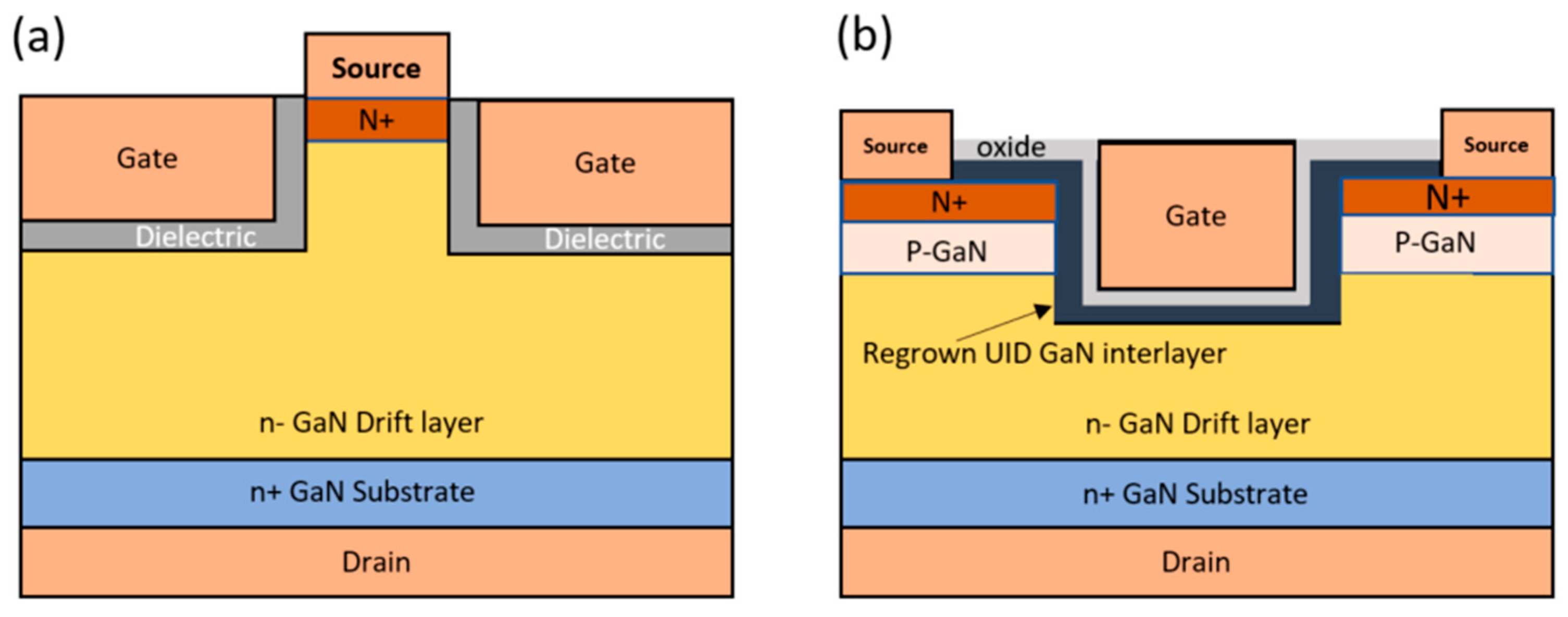
3. Vertical GaN Field Effect Transistors
4. Techniques to Boost the Breakdown Voltage
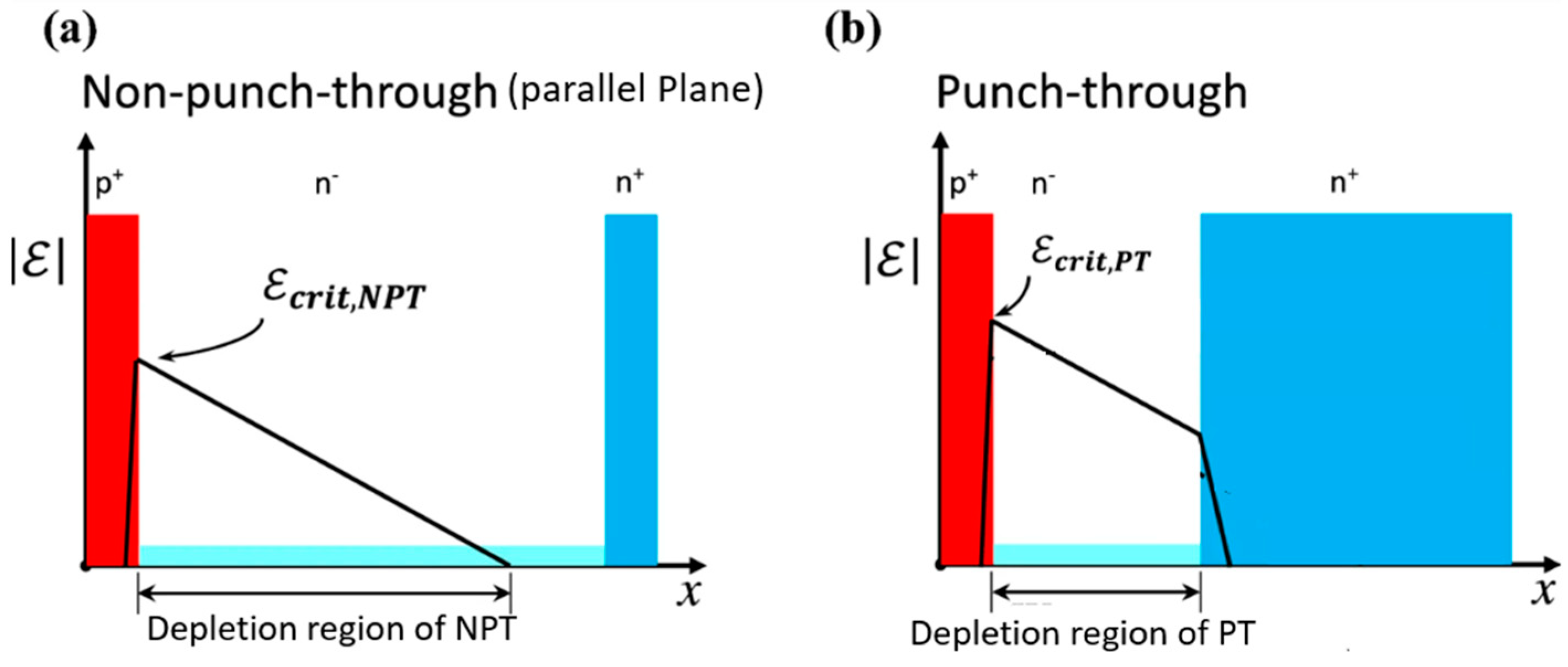
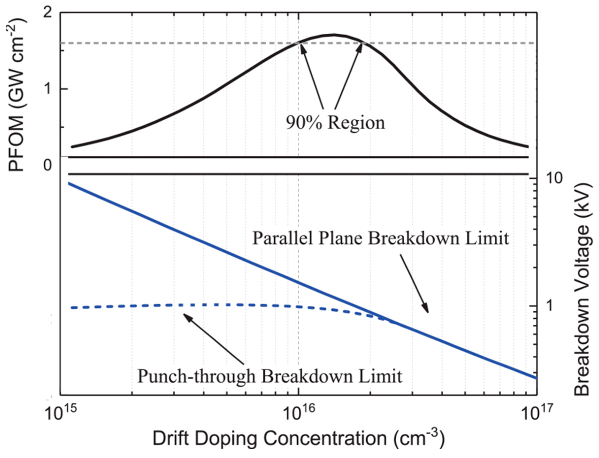
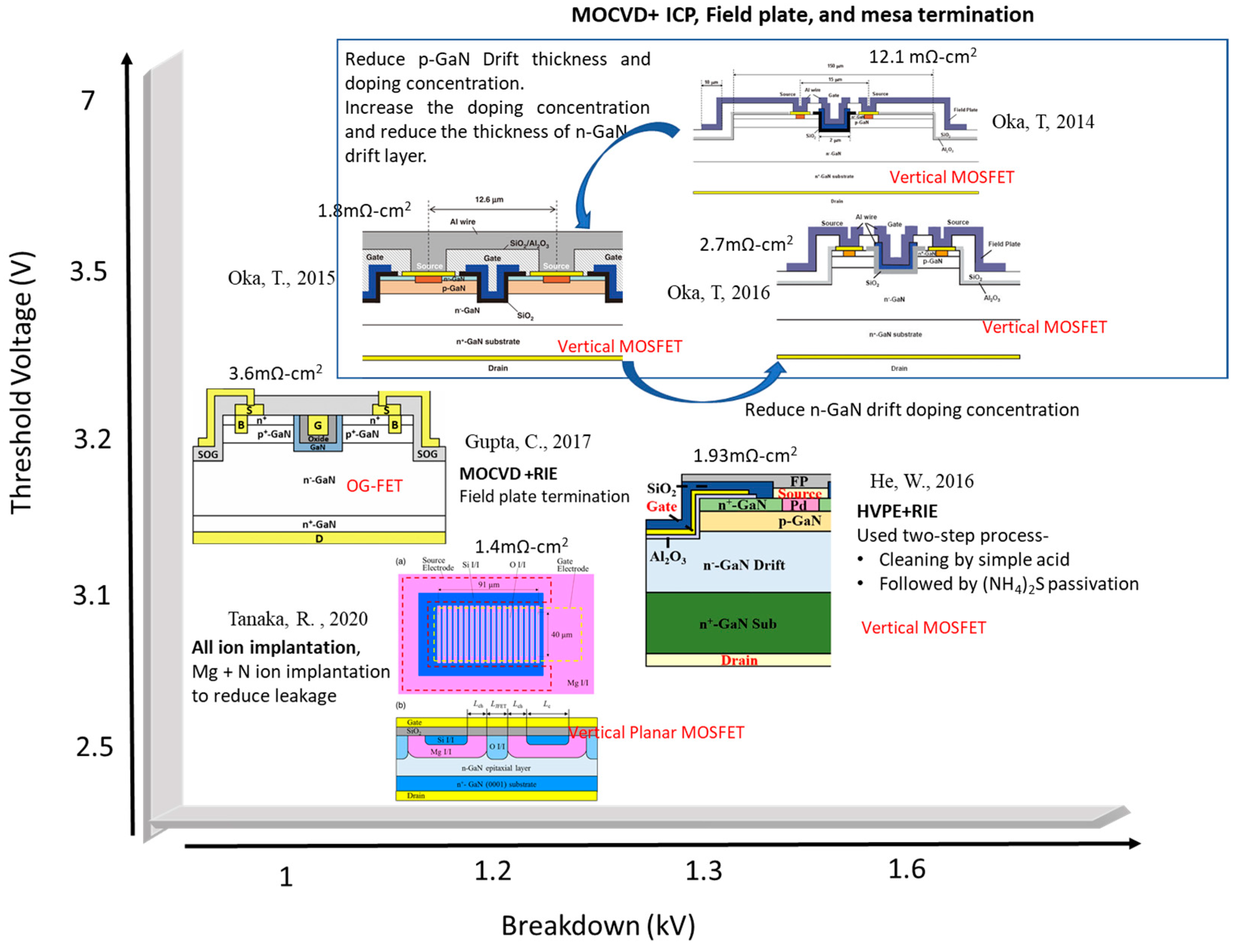
4.1. Drift Layer Thickness and Doping Concentration
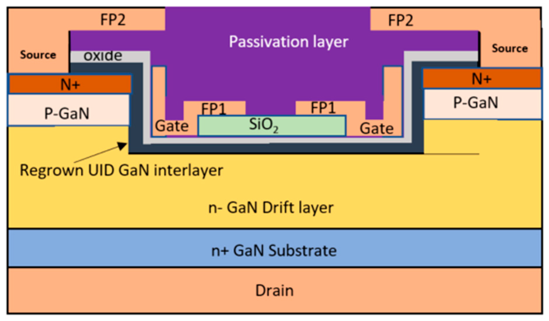
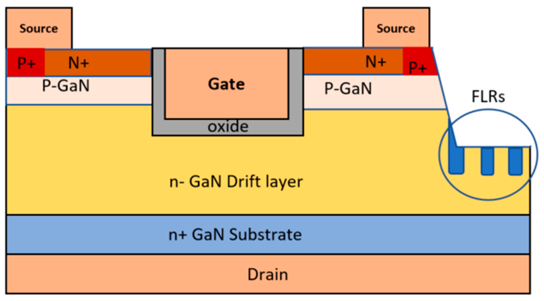
4.2. Field Plate Termination
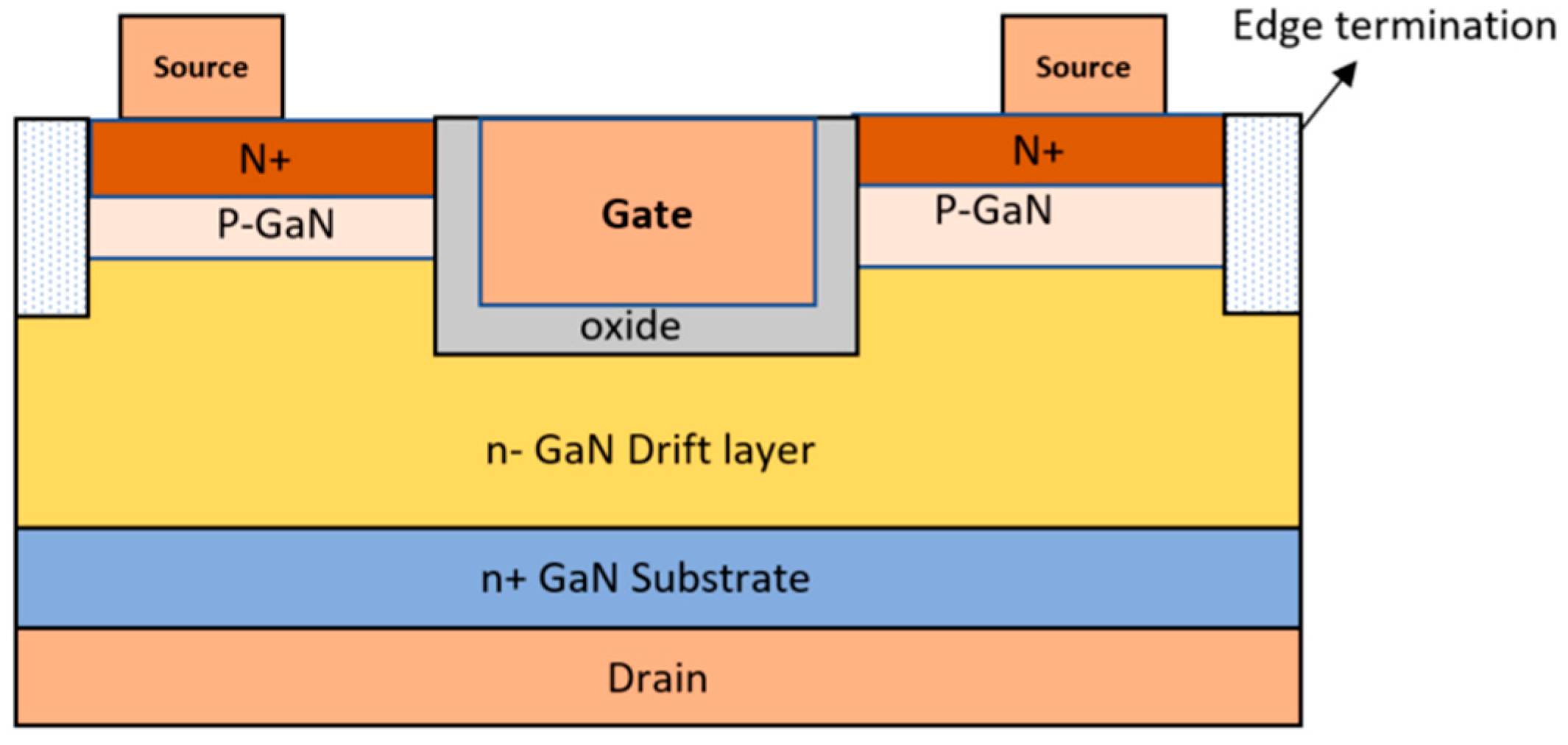
4.3. Edge Termination
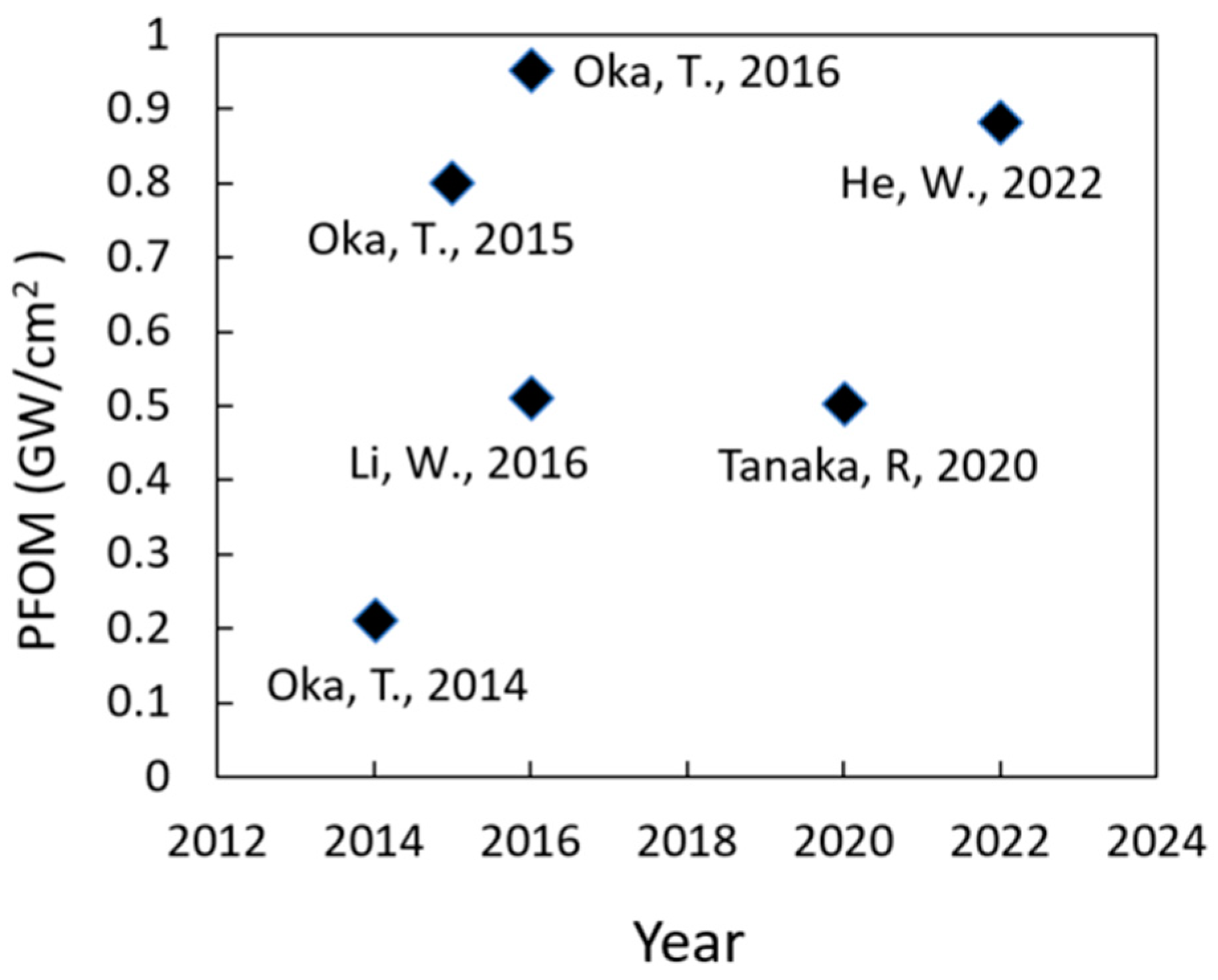
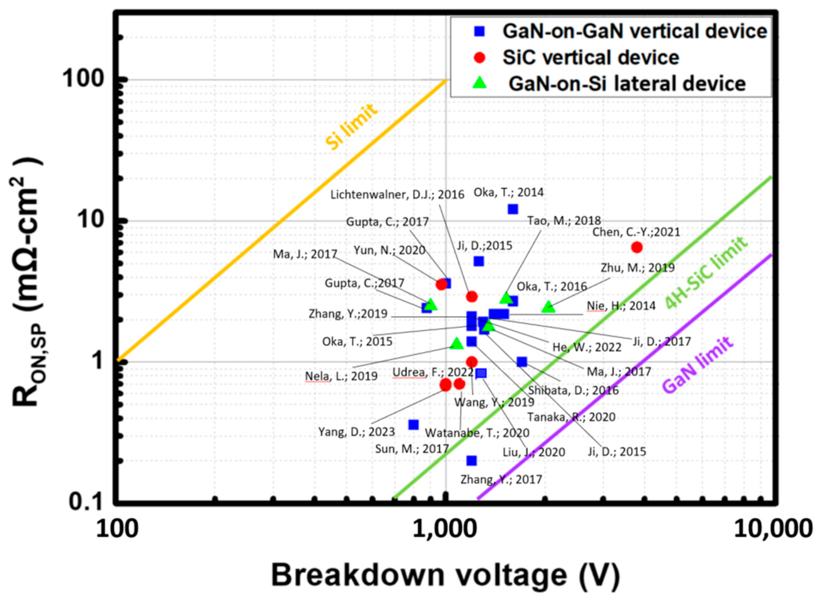
5. GaN Vertical Transistor Summary and Benchmarking
6. Conclusions
Author Contributions
Funding
Data Availability Statement
Acknowledgments
Conflicts of Interest
References
- Chow, T.P.; Omura, I.; Higashiwaki, M.; Kawarada, H.; Pala, V. Smart Power Devices and ICs Using GaAs and Wide and Extreme Bandgap Semiconductors. IEEE Trans. Electron Devices 2017, 64, 856–873. [Google Scholar] [CrossRef]
- Baliga, B.J. Trends in power semiconductor devices. IEEE Trans. Electron Devices 1996, 43, 1717–1731. [Google Scholar] [CrossRef]
- Chow, T.P. Wide bandgap semiconductor power devices for energy efficient systems. In Proceedings of the 2015 IEEE 3rd Workshop on Wide Bandgap Power Devices and Applications (WiPDA), Blacksburg, VA, USA, 2–4 November 2015; pp. 402–405. [Google Scholar]
- Ding, X.; Zhou, Y.; Cheng, J. A review of gallium nitride power device and its applications in motor drive. CES Trans. Electr. Mach. Syst. 2019, 3, 54–64. [Google Scholar] [CrossRef]
- Rodríguez, M.; Zhang, Y.; Maksimović, D. High-frequency PWM buck converters using GaN-on-SiC HEMTs. IEEE Trans. Power Electron. 2013, 29, 2462–2473. [Google Scholar] [CrossRef]
- Meneghini, M.; De Santi, C.; Abid, I.; Buffolo, M.; Cioni, M.; Khadar, R.A.; Nela, L.; Zagni, N.; Chini, A.; Medjdoub, F. GaN-based power devices: Physics, reliability, and perspectives. J. Appl. Phys. 2021, 130, 181101. [Google Scholar] [CrossRef]
- EPC2023—Enhancement Mode Power Transistor. Available online: https://epc-co.com/epc/Portals/0/epc/documents/datasheets/EPC2023_datasheet.pdf (accessed on 20 June 2023).
- EPC2012C—Enhancement Mode Power Transistor. Available online: https://epc-co.com/epc/Products/eGaNFETsandICs/EPC2012C.aspx (accessed on 20 June 2023).
- EPC2108—Enhancement-Mode GaN Power Transistor Half-Bridge with Integrated Synchronous Bootstrap. Available online: https://epc-co.com/epc/Portals/0/epc/documents/datasheets/EPC2108_datasheet.pdf (accessed on 20 June 2023).
- EPC launches 200V, 10mΩ GaN FET. Available online: https://www.semiconductor-today.com/news_items/2023/jan/epc-310123.shtml (accessed on 20 June 2023).
- TP65H480G4JSGB-650V SuperGaN® GaN FET in PQFN (source tab). Available online: https://www.transphormusa.com/en/document/datasheet-tp65h480g4jsgb-650v-gan-fet (accessed on 20 June 2023).
- TP65H050G4BS-650V SuperGaN® FET in TO-263 (source tab). Available online: https://www.transphormusa.com/en/document/datasheet-tp65h050g4bs-650v-gan-fet (accessed on 20 June 2023).
- 900V Cascode GaN FET in TO-247 (Source Tab). Available online: https://www.transphormusa.com/en/document/datasheet-tp90h050ws/ (accessed on 20 June 2023).
- Hwang, I.; Choi, H.; Lee, J.; Choi, H.S.; Kim, J.; Ha, J.; Um, C.Y.; Hwang, S.K.; Oh, J.; Kim, J.Y.; et al. 1.6kV, 2.9 mΩ cm2 normally-off p-GaN HEMT device. In Proceedings of the 2012 24th International Symposium on Power Semiconductor Devices and ICs, Bruges, Belgium, 3–7 June 2012; pp. 41–44. [Google Scholar]
- Dogmus, E.; Zegaoui, M.; Medjdoub, F. GaN-on-silicon high-electron-mobility transistor technology with ultra-low leakage up to 3000 V using local substrate removal and AlN ultra-wide bandgap. Appl. Phys. Express 2018, 11, 034102. [Google Scholar] [CrossRef]
- Herbecq, N.; Roch-Jeune, I.; Linge, A.; Zegaoui, M.; Jeannin, P.-O.; Rouger, N.; Medjdoub, F. Above 2000 V breakdown voltage at 600 K GaN-on-silicon high electron mobility transistors. Phys. Status Solidi (A) 2016, 213, 873–877. [Google Scholar] [CrossRef]
- Xiao, M.; Ma, Y.; Du, Z.; Pathirana, V.; Cheng, K.; Xie, A.; Beam, E.; Cao, Y.; Udrea, F.; Wang, H.; et al. Multi-Channel Monolithic-Cascode HEMT (MC2-HEMT): A New GaN Power Switch up to 10 kV. In Proceedings of the 2021 IEEE International Electron Devices Meeting (IEDM), San Francisco, CA, USA, 11–16 December 2021; pp. 5.5.1–5.5.4. [Google Scholar]
- Zhang, Y. Stretching GaN Power Devices to 10 kV. Available online: https://compoundsemiconductor.net/article/115524/Stretching_GaN_power_devices_to_10_kV (accessed on 20 June 2023).
- Hsu, L.-H.; Lai, Y.-Y.; Tu, P.-T.; Langpoklakpam, C.; Chang, Y.-T.; Huang, Y.-W.; Lee, W.-C.; Tzou, A.-J.; Cheng, Y.-J.; Lin, C.-H. Development of GaN HEMTs fabricated on silicon, silicon-on-insulator, and engineered substrates and the heterogeneous integration. Micromachines 2021, 12, 1159. [Google Scholar] [CrossRef]
- Zhou, S.Q.; Vantomme, A.; Zhang, B.S.; Yang, H.; Wu, M.F. Comparison of the properties of GaN grown on complex Si-based structures. Appl. Phys. Lett. 2005, 86, 081912. [Google Scholar] [CrossRef]
- Dadgar, A.; Schulze, F.; Wienecke, M.; Gadanecz, A.; Bläsing, J.; Veit, P.; Hempel, T.; Diez, A.; Christen, J.; Krost, A. Epitaxy of GaN on silicon—Impact of symmetry and surface reconstruction. New J. Phys. 2007, 9, 389. [Google Scholar] [CrossRef]
- Zhao, D.; Zhao, D. Analysis of the growth of GaN epitaxy on silicon. J. Semicond. 2018, 39, 033006. [Google Scholar] [CrossRef]
- Wośko, M.; Szymański, T.; Paszkiewicz, B.; Pokryszka, P.; Paszkiewicz, R. MOVPE growth conditions optimization for AlGaN/GaN/Si heterostructures with SiN and LT-AlN interlayers designed for HEMT applications. J. Mater. Sci. Mater. Electron. 2019, 30, 4111–4116. [Google Scholar] [CrossRef]
- Stanchu, H.V.; Kuchuk, A.V.; Mazur, Y.I.; Li, C.; Lytvyn, P.M.; Schmidbauer, M.; Maidaniuk, Y.; Benamara, M.; Ware, M.E.; Wang, Z.M. Local strain and crystalline defects in GaN/AlGaN/GaN (0001) heterostructures induced by compositionally graded AlGaN buried layers. Cryst. Growth Des. 2018, 19, 200–210. [Google Scholar] [CrossRef]
- Ibbetson, J.P.; Fini, P.T.; Ness, K.D.; DenBaars, S.P.; Speck, J.S.; Mishra, U.K. Polarization effects, surface states, and the source of electrons in AlGaN/GaN heterostructure field effect transistors. Appl. Phys. Lett. 2000, 77, 250–252. [Google Scholar] [CrossRef]
- del Alamo, J.A.; Joh, J. GaN HEMT reliability. Microelectron. Reliab. 2009, 49, 1200–1206. [Google Scholar] [CrossRef]
- Ohki, T.; Kikkawa, T.; Inoue, Y.; Kanamura, M.; Okamoto, N.; Makiyama, K.; Imanishi, K.; Shigematsu, H.; Joshin, K.; Hara, N. Reliability of GaN HEMTs: Current status and future technology. In Proceedings of the 2009 IEEE International Reliability Physics Symposium, Montreal, QC, Canada, 26–30 April 2009; pp. 61–70. [Google Scholar]
- Saito, W. Reliability of GaN-HEMTs for high-voltage switching applications. In Proceedings of the 2011 International Reliability Physics Symposium, Monterey, CA, USA, 10–14 April 2011; pp. 4E.1.1–4E.1.5. [Google Scholar]
- Meneghesso, G.; Verzellesi, G.; Danesin, F.; Rampazzo, F.; Zanon, F.; Tazzoli, A.; Meneghini, M.; Zanoni, E. Reliability of GaN High-Electron-Mobility Transistors: State of the Art and Perspectives. IEEE Trans. Device Mater. Reliab. 2008, 8, 332–343. [Google Scholar] [CrossRef]
- Chen, K.J.; Zhou, C. Enhancement-mode AlGaN/GaN HEMT and MIS-HEMT technology. Phys. Status Solidi (A) 2011, 208, 434–438. [Google Scholar] [CrossRef]
- Chen, K.J.; Yuan, L.; Wang, M.J.; Chen, H.; Huang, S.; Zhou, Q.; Zhou, C.; Li, B.K.; Wang, J.N. Physics of fluorine plasma ion implantation for GaN normally-off HEMT technology. In Proceedings of the 2011 International Electron Devices Meeting, Washington, DC, USA, 5–7 December 2011; pp. 19.14.11–19.14.14. [Google Scholar]
- Yong, C.; Yugang, Z.; Chen, K.J.; Lau, K.M. High-performance enhancement-mode AlGaN/GaN HEMTs using fluoride-based plasma treatment. IEEE Electron Device Lett. 2005, 26, 435–437. [Google Scholar] [CrossRef]
- Saito, W.; Takada, Y.; Kuraguchi, M.; Tsuda, K.; Omura, I. Recessed-gate structure approach toward normally off high-Voltage AlGaN/GaN HEMT for power electronics applications. IEEE Trans. Electron Devices 2006, 53, 356–362. [Google Scholar] [CrossRef]
- Greco, G.; Iucolano, F.; Roccaforte, F. Review of technology for normally-off HEMTs with p-GaN gate. Mater. Sci. Semicond. Process. 2018, 78, 96–106. [Google Scholar] [CrossRef]
- Ma, J.; Matioli, E. High Performance Tri-Gate GaN Power MOSHEMTs on Silicon Substrate. IEEE Electron Device Lett. 2017, 38, 367–370. [Google Scholar] [CrossRef]
- Ma, J.; Matioli, E. Slanted tri-gates for high-voltage GaN power devices. IEEE Electron Device Lett. 2017, 38, 1305–1308. [Google Scholar] [CrossRef]
- Zhang, W.; Xu, Z.; Zhang, Z.; Wang, F.; Tolbert, L.M.; Blalock, B.J. Evaluation of 600 V cascode GaN HEMT in device characterization and all-GaN-based LLC resonant converter. In Proceedings of the 2013 IEEE Energy Conversion Congress and Exposition, Denver, CO, USA, 15–19 September 2013; pp. 3571–3578. [Google Scholar]
- Huang, X.; Liu, Z.; Li, Q.; Lee, F.C. Evaluation and Application of 600 V GaN HEMT in Cascode Structure. IEEE Trans. Power Electron. 2014, 29, 2453–2461. [Google Scholar] [CrossRef]
- Zhong, Y.; Zhang, J.; Wu, S.; Jia, L.; Yang, X.; Liu, Y.; Zhang, Y.; Sun, Q. A review on the GaN-on-Si power electronic devices. Fundam. Res. 2022, 2, 462–475. [Google Scholar] [CrossRef]
- Nexgenpowersystems. Vertical GaN™ Theory of Operation. Available online: https://nexgenpowersystems.com/wp-content/uploads/2020/03/Theory_of_operation_TOC_r8.6.pdf (accessed on 1 July 2023).
- Oka, T.; Ueno, Y.; Ina, T.; Hasegawa, K. Vertical GaN-based trench metal oxide semiconductor field-effect transistors on a free-standing GaN substrate with blocking voltage of 1.6 kV. Appl. Phys. Express 2014, 7, 021002. [Google Scholar] [CrossRef]
- Kizilyalli, I.C.; Edwards, A.P.; Nie, H.; Disney, D.; Bour, D. High Voltage Vertical GaN p-n Diodes with Avalanche Capability. IEEE Trans. Electron Devices 2013, 60, 3067–3070. [Google Scholar] [CrossRef]
- Santi, C.D.; Fabris, E.; Meneghesso, G.; Zanoni, E.; Meneghini, M. GaN Vertical p–i–n Diodes in Avalanche Regime: Time-Dependent Behavior and Degradation. IEEE Electron Device Lett. 2020, 41, 1300–1303. [Google Scholar] [CrossRef]
- Maeda, T.; Narita, T.; Ueda, H.; Kanechika, M.; Uesugi, T.; Kachi, T.; Kimoto, T.; Horita, M.; Suda, J. Design and Fabrication of GaN p-n Junction Diodes with Negative Beveled-Mesa Termination. IEEE Electron Device Lett. 2019, 40, 941–944. [Google Scholar] [CrossRef]
- Oka, T. Recent development of vertical GaN power devices. Jpn. J. Appl. Phys. 2019, 58, SB0805. [Google Scholar] [CrossRef]
- Sochacki, T.; Bryan, Z.; Amilusik, M.; Bobea, M.; Fijalkowski, M.; Bryan, I.; Lucznik, B.; Collazo, R.; Weyher, J.L.; Kucharski, R.; et al. HVPE-GaN grown on MOCVD-GaN/sapphire template and ammonothermal GaN seeds: Comparison of structural, optical, and electrical properties. J. Cryst. Growth 2014, 394, 55–60. [Google Scholar] [CrossRef]
- Mizutani, T.; Ohno, Y.; Akita, M.; Kishimoto, S.; Maezawa, K. A study on current collapse in AlGaN/GaN HEMTs induced by bias stress. Electron Devices IEEE Trans. 2003, 50, 2015–2020. [Google Scholar] [CrossRef]
- Yu, C.; Luo, X.D.; Zhou, W.; Luo, Q.Z.; Liu, P.s. Investigation on the current collapse effect of AlGaN/GaN/InGaN/GaN doubleheterojunction HEMTs. Wuli Xuebao/Acta Phys. Sin. 2012, 61, 207301. [Google Scholar]
- Yaegassi, S.; Okada, M.; Saitou, Y.; Yokoyama, M.; Nakata, K.; Katayama, K.; Ueno, M.; Kiyama, M.; Katsuyama, T.; Nakamura, T. Vertical heterojunction field-effect transistors utilizing re-grown AlGaN/GaN two-dimensional electron gas channels on GaN substrates. Phys. Status Solidi (C) 2011, 8, 450–452. [Google Scholar] [CrossRef]
- Chen, K.J.; Häberlen, O.; Lidow, A.; Tsai, C.l.; Ueda, T.; Uemoto, Y.; Wu, Y. GaN-on-Si Power Technology: Devices and Applications. IEEE Trans. Electron Devices 2017, 64, 779–795. [Google Scholar] [CrossRef]
- Li, Y.; Yang, S.; Liu, K.; Cheng, K.; Sheng, K.; Shen, B. Low ON-Resistance Fully-Vertical GaN-on-SiC Schottky Barrier Diode with Conductive Buffer Layer. In Proceedings of the 2022 IEEE 34th International Symposium on Power Semiconductor Devices and ICs (ISPSD), Vancouver, BC, Canada, 22–25 May 2022; pp. 333–336. [Google Scholar]
- Li, Y.; Yang, S.; Liu, K.; Cheng, K.; Sheng, K.; Shen, B. Fully-Vertical GaN-on-SiC Schottky Barrier Diode: Role of Conductive Buffer Structure. IEEE Trans. Electron Devices 2023, 70, 619–626. [Google Scholar] [CrossRef]
- Liu, J.; Xiao, M.; Zhang, R.; Pidaparthi, S.; Cui, H.; Edwards, A.; Craven, M.; Baubutr, L.; Drowley, C.; Zhang, Y. 1.2-kV Vertical GaN Fin-JFETs: High-Temperature Characteristics and Avalanche Capability. IEEE Trans. Electron Devices 2021, 68, 2025–2032. [Google Scholar] [CrossRef]
- Liu, J.; Zhang, R.; Xiao, M.; Pidaparthi, S.; Cui, H.; Edwards, A.; Baubutr, L.; Drowley, C.; Zhang, Y. Surge Current and Avalanche Ruggedness of 1.2-kV Vertical GaN p-n Diodes. IEEE Trans. Power Electron. 2021, 36, 10959–10964. [Google Scholar] [CrossRef]
- Zhang, Y.; Dadgar, A.; Palacios, T. Gallium nitride vertical power devices on foreign substrates: A review and outlook. J. Phys. D Appl. Phys. 2018, 51, 273001. [Google Scholar] [CrossRef]
- Khadar, R.A.; Liu, C.; Zhang, L.; Xiang, P.; Cheng, K.; Matioli, E. 820-V GaN-on-Si Quasi-Vertical p-i-n Diodes with BFOM of 2.0 GW/cm2. IEEE Electron Device Lett. 2018, 39, 401–404. [Google Scholar] [CrossRef]
- Kizilyalli, I.C.; Edwards, A.P.; Aktas, O.; Prunty, T.; Bour, D. Vertical power pn diodes based on bulk GaN. IEEE Trans. Electron Devices 2014, 62, 414–422. [Google Scholar] [CrossRef]
- Ohta, H.; Kaneda, N.; Horikiri, F.; Narita, Y.; Yoshida, T.; Mishima, T.; Nakamura, T. Vertical GaN pn junction diodes with high breakdown voltages over 4 kV. IEEE Electron Device Lett. 2015, 36, 1180–1182. [Google Scholar] [CrossRef]
- Tanaka, R.; Takashima, S.; Ueno, K.; Matsuyama, H.; Edo, M. Demonstration of 1200 V/1.4 mΩ cm2 vertical GaN planar MOSFET fabricated by an all ion implantation process. Jpn. J. Appl. Phys. 2020, 59, SGGD02. [Google Scholar] [CrossRef]
- Tanaka, R.; Takashima, S.; Ueno, K.; Matsuyama, H.; Edo, M.; Nakagawa, K. Mg implantation dose dependence of MOS channel characteristics in GaN double-implanted MOSFETs. Appl. Phys. Express 2019, 12, 054001. [Google Scholar] [CrossRef]
- Ben-Yaacov, I.; Seck, Y.-K.; Mishra, U.K.; DenBaars, S.P. AlGaN/GaN current aperture vertical electron transistors with regrown channels. J. Appl. Phys. 2004, 95, 2073–2078. [Google Scholar] [CrossRef]
- Williams, R.K.; Darwish, M.N.; Blanchard, R.A.; Siemieniec, R.; Rutter, P.; Kawaguchi, Y. The trench power MOSFET: Part I—History, technology, and prospects. IEEE Trans. Electron Devices 2017, 64, 674–691. [Google Scholar] [CrossRef]
- Williams, R.K.; Darwish, M.N.; Blanchard, R.A.; Siemieniec, R.; Rutter, P.; Kawaguchi, Y. The trench power MOSFET—Part II: Application specific VDMOS, LDMOS, packaging, and reliability. IEEE Trans. Electron Devices 2017, 64, 692–712. [Google Scholar] [CrossRef]
- Otake, H.; Egami, S.; Ohta, H.; Nanishi, Y.; Takasu, H. GaN-Based Trench Gate Metal Oxide Semiconductor Field Effect Transistors with Over 100 cm2/(V s) Channel Mobility. Jpn. J. Appl. Phys. 2007, 46, L599. [Google Scholar] [CrossRef]
- Otake, H.; Chikamatsu, K.; Yamaguchi, A.; Fujishima, T.; Ohta, H. Vertical GaN-Based Trench Gate Metal Oxide Semiconductor Field-Effect Transistors on GaN Bulk Substrates. Appl. Phys. Express 2008, 1, 011105. [Google Scholar] [CrossRef]
- Oka, T.; Ina, T.; Ueno, Y.; Nishii, J.J.A.P.E. 1.8 mΩ·cm2 vertical GaN-based trench metal–oxide–semiconductor field-effect transistors on a free-standing GaN substrate for 1.2-kV-class operation. Appl. Phys. Express 2015, 8, 054101. [Google Scholar] [CrossRef]
- Oka, T.; Ina, T.; Ueno, Y.; Nishii, J. Over 10 a operation with switching characteristics of 1.2 kV-class vertical GaN trench MOSFETs on a bulk GaN substrate. In Proceedings of the 2016 28th International Symposium on Power Semiconductor Devices and ICs (ISPSD), Prague, Czech Republic, 12–16 June 2016; pp. 459–462. [Google Scholar]
- Li, W.; Chowdhury, S. Design and fabrication of a 1.2 kV GaN-based MOS vertical transistor for single chip normally off operation. Phys. Status Solidi (A) 2016, 213, 2714–2720. [Google Scholar] [CrossRef]
- He, W.; Li, J.; Liao, Z.; Lin, F.; Wu, J.; Wang, B.; Wang, M.; Liu, N.; Chiu, H.-C.; Kuo, H.-C.; et al. 1.3 kV Vertical GaN-Based Trench MOSFETs on 4-Inch Free Standing GaN Wafer. Nanoscale Res. Lett. 2022, 17, 14. [Google Scholar] [CrossRef] [PubMed]
- Fu, H.; Fu, K.; Chowdhury, S.; Palacios, T.; Zhao, Y. Vertical GaN Power Devices: Device Principles and Fabrication Technologies—Part II. IEEE Trans. Electron Devices 2021, 68, 3212–3222. [Google Scholar] [CrossRef]
- Sun, M.; Zhang, Y.; Gao, X.; Palacios, T. High-Performance GaN Vertical Fin Power Transistors on Bulk GaN Substrates. IEEE Electron Device Lett. 2017, 38, 509–512. [Google Scholar] [CrossRef]
- Zhang, Y.; Sun, M.; Piedra, D.; Hu, J.; Liu, Z.; Lin, Y.; Gao, X.; Shepard, K.; Palacios, T. 1200 V GaN vertical fin power field-effect transistors. In Proceedings of the 2017 IEEE International Electron Devices Meeting (IEDM), San Francisco, CA, USA, 2–6 December 2017; pp. 9.2.1–9.2.4. [Google Scholar]
- Ji, D.; Gupta, C.; Chan, S.H.; Agarwal, A.; Li, W.; Keller, S.; Mishra, U.K.; Chowdhury, S. Demonstrating> 1.4 kV OG-FET performance with a novel double field-plated geometry and the successful scaling of large-area devices. In Proceedings of the 2017 IEEE International Electron Devices Meeting (IEDM), San Francisco, CA, USA, 2–6 December 2017; pp. 9.4.1–9.4.4. [Google Scholar]
- Ji, D.; Gupta, C.; Agarwal, A.; Chan, S.H.; Lund, C.; Li, W.; Keller, S.; Mishra, U.K.; Chowdhury, S. Large-Area In-Situ Oxide, GaN Interlayer-Based Vertical Trench MOSFET (OG-FET). IEEE Electron Device Lett. 2018, 39, 711–714. [Google Scholar] [CrossRef]
- Ji, D.; Li, W.; Chowdhury, S. A study on the impact of channel mobility on switching performance of vertical GaN MOSFETs. IEEE Trans. Electron Devices 2018, 65, 4271–4275. [Google Scholar] [CrossRef]
- Ruzzarin, M.; Geens, K.; Borga, M.; Liang, H.; You, S.; Bakeroot, B.; Decoutere, S.; De Santi, C.; Neviani, A.; Meneghini, M.; et al. Exploration of gate trench module for vertical GaN devices. Microelectron. Reliab. 2020, 114, 113828. [Google Scholar] [CrossRef]
- Robertson, J.; Falabretti, B. Band offsets of high K gate oxides on III-V semiconductors. J. Appl. Phys. 2006, 100, 014111. [Google Scholar] [CrossRef]
- Gupta, C.; Chan, S.H.; Pasayat, S.S.; Keller, S.; Mishra, U.K. Reverse breakdown studies of GaN MOSCAPs and their implications in vertical GaN power devices. J. Appl. Phys. 2019, 125, 124101. [Google Scholar] [CrossRef]
- Fu, H.; Huang, X.; Chen, H.; Lu, Z.; Zhang, X.; Zhao, Y. Effect of buffer layer design on vertical GaN-on-GaN pn and Schottky power diodes. IEEE Electron Device Lett. 2017, 38, 763–766. [Google Scholar] [CrossRef]
- Shuji Nakamura, S.N. GaN Growth Using GaN Buffer Layer. Jpn. J. Appl. Phys. 1991, 30, L1705. [Google Scholar] [CrossRef]
- Kuznia, J.N.; Khan, M.A.; Olson, D.T.; Kaplan, R.; Freitas, J. Influence of buffer layers on the deposition of high quality single crystal GaN over sapphire substrates. J. Appl. Phys. 1993, 73, 4700–4702. [Google Scholar] [CrossRef]
- Arulkumaran, S.; Egawa, T.; Matsui, S.; Ishikawa, H. Enhancement of breakdown voltage by AlN buffer layer thickness in AlGaN/GaN high-electron-mobility transistors on 4in. diameter silicon. Appl. Phys. Lett. 2005, 86, 123503. [Google Scholar] [CrossRef]
- Baliga, B.J. Power semiconductor device figure of merit for high-frequency applications. IEEE Electron Device Lett. 1989, 10, 455–457. [Google Scholar] [CrossRef]
- Huang, A.Q. New unipolar switching power device figures of merit. IEEE Electron Device Lett. 2004, 25, 298–301. [Google Scholar] [CrossRef]
- Brusaterra, E.; Treidel, E.B.; Brunner, F.; Wolf, M.; Thies, A.; Würfl, J.; Hilt, O. Optimization of Vertical GaN Drift Region Layers for Avalanche and Punch-Through Pn-Diodes. IEEE Electron Device Lett. 2023, 44, 388–391. [Google Scholar] [CrossRef]
- Mnatsakanov, T.T.; Levinshtein, M.E.; Pomortseva, L.I.; Yurkov, S.N.; Simin, G.S.; Asif Khan, M. Carrier mobility model for GaN. Solid-State Electron. 2003, 47, 111–115. [Google Scholar] [CrossRef]
- Bahat-Treidel, E. GaN-Based HEMTs for High Voltage Operation: Design, Technology and Characterization; Cuvillier Verlag: Goettingen, Germany, 2012; Volume 22. [Google Scholar]
- Slobodyan, O.; Flicker, J.; Dickerson, J.; Shoemaker, J.; Binder, A.; Smith, T.; Goodnick, S.; Kaplar, R.; Hollis, M. Analysis of the dependence of critical electric field on semiconductor bandgap. J. Mater. Res. 2022, 37, 849–865. [Google Scholar] [CrossRef]
- Maeda, T.; Narita, T.; Yamada, S.; Kachi, T.; Kimoto, T.; Horita, M.; Suda, J. Impact ionization coefficients and critical electric field in GaN. J. Appl. Phys. 2021, 129, 185702. [Google Scholar] [CrossRef]
- Baliga, B.J. Fundamentals of Power Semiconductor Devices; Springer Science & Business Media: Berlin/Heidelberg, Germany, 2010. [Google Scholar]
- Chyi, J.-I.; Lee, C.M.; Chuo, C.-C.; Chi, G.C.; Dang, G.; Zhang, A.P.; Ren, F.; Cao, X.A.; Pearton, S.J.; Chu, G.; et al. Growth and Device Performance of GaN Schottky Rectifiers. MRS Internet J. Nitride Semicond. Res. 1999, 4, E8. [Google Scholar] [CrossRef]
- Karmalkar, S.; Mishra, U.K. Enhancement of breakdown voltage in AlGaN/GaN high electron mobility transistors using a field plate. IEEE Trans. Electron Devices 2001, 48, 1515–1521. [Google Scholar] [CrossRef]
- Huili, X.; Dora, Y.; Chini, A.; Heikman, S.; Keller, S.; Mishra, U.K. High breakdown voltage AlGaN-GaN HEMTs achieved by multiple field plates. IEEE Electron Device Lett. 2004, 25, 161–163. [Google Scholar] [CrossRef]
- Karmalkar, S.; Shur, M.S.; Simin, G.; Khan, M.A. Field-plate engineering for HFETs. IEEE Trans. Electron Devices 2005, 52, 2534–2540. [Google Scholar] [CrossRef]
- Lei, Y.; Shi, H.; Lu, H.; Chen, D.; Zhang, R.; Zheng, Y. Field plate engineering for GaN-based Schottky barrier diodes. J. Semicond. 2013, 34, 054007. [Google Scholar] [CrossRef]
- Chowdhury, S. 6—GaN-on-GaN power device design and fabrication. In Wide Bandgap Semiconductor Power Devices; Baliga, B.J., Ed.; Woodhead Publishing: Sawston, UK, 2019; pp. 209–248. [Google Scholar] [CrossRef]
- Anantharam, V.; Bhat, K.N. Analytical solutions for the breakdown voltages of punched-through diodes having curved junction boundaries at the edges. IEEE Trans. Electron Devices 1980, 27, 939–945. [Google Scholar] [CrossRef]
- Fu, H.; Fu, K.; Chowdhury, S.; Palacios, T.; Zhao, Y. Vertical GaN Power Devices: Device Principles and Fabrication Technologies—Part I. IEEE Trans. Electron Devices 2021, 68, 3200–3211. [Google Scholar] [CrossRef]
- Wierer, J.J.; Dickerson, J.R.; Allerman, A.A.; Armstrong, A.M.; Crawford, M.H.; Kaplar, R.J. Simulations of Junction Termination Extensions in Vertical GaN Power Diodes. IEEE Trans. Electron Devices 2017, 64, 2291–2297. [Google Scholar] [CrossRef]
- Zeng, K.; Chowdhury, S. Designing Beveled Edge Termination in GaN Vertical p-i-n Diode-Bevel Angle, Doping, and Passivation. IEEE Trans. Electron Devices 2020, 67, 2457–2462. [Google Scholar] [CrossRef]
- Sung, W.; Brunt, E.V.; Baliga, B.J.; Huang, A.Q. A New Edge Termination Technique for High-Voltage Devices in 4H-SiC–Multiple-Floating-Zone Junction Termination Extension. IEEE Electron Device Lett. 2011, 32, 880–882. [Google Scholar] [CrossRef]
- Ozbek, A.M.; Baliga, B.J. Planar Nearly Ideal Edge-Termination Technique for GaN Devices. IEEE Electron Device Lett. 2011, 32, 300–302. [Google Scholar] [CrossRef]
- Wang, J.; Cao, L.; Xie, J.; Beam, E.; McCarthy, R.; Youtsey, C.; Fay, P. High voltage vertical p-n diodes with ion-implanted edge termination and sputtered SiNx passivation on GaN substrates. In Proceedings of the 2017 IEEE International Electron Devices Meeting (IEDM), San Francisco, CA, USA, 2–6 December 2017; pp. 9.6.1–9.6.4. [Google Scholar]
- Dickerson, J.R.; Allerman, A.A.; Bryant, B.N.; Fischer, A.J.; King, M.P.; Moseley, M.W.; Armstrong, A.M.; Kaplar, R.J.; Kizilyalli, I.C.; Aktas, O.; et al. Vertical GaN Power Diodes with a Bilayer Edge Termination. IEEE Trans. Electron Devices 2016, 63, 419–425. [Google Scholar] [CrossRef]
- Shurrab, M.; Siddiqui, A.; Singh, S. Counter-Doped Multizone Junction Termination Extension Structures in Vertical GaN Diodes. IEEE J. Electron Devices Soc. 2019, 7, 287–294. [Google Scholar] [CrossRef]
- Kachi, T.; Narita, T.; Sakurai, H.; Matys, M.; Kataoka, K.; Hirukawa, K.; Sumida, K.; Horita, M.; Ikarashi, N.; Sierakowski, K.; et al. Process engineering of GaN power devices via selective-area p-type doping with ion implantation and ultra-high-pressure annealing. J. Appl. Phys. 2022, 132, 130901. [Google Scholar] [CrossRef]
- Anderson, T.J.; Feigelson, B.N.; Kub, F.J.; Tadjer, M.J.; Hobart, K.D.; Mastro, M.A.; Hite, J.K.; Eddy, C.R., Jr. Activation of Mg implanted in GaN by multicycle rapid thermal annealing. Electron. Lett. 2014, 50, 197–198. [Google Scholar] [CrossRef]
- Fukushima, H.; Usami, S.; Ogura, M.; Ando, Y.; Tanaka, A.; Deki, M.; Kushimoto, M.; Nitta, S.; Honda, Y.; Amano, H. Vertical GaN p–n diode with deeply etched mesa and the capability of avalanche breakdown. Appl. Phys. Express 2019, 12, 026502. [Google Scholar] [CrossRef]
- Fukushima, H.; Usami, S.; Ogura, M.; Ando, Y.; Tanaka, A.; Deki, M.; Kushimoto, M.; Nitta, S.; Honda, Y.; Amano, H. Deeply and vertically etched butte structure of vertical GaN p–n diode with avalanche capability. Jpn. J. Appl. Phys. 2019, 58, SCCD25. [Google Scholar] [CrossRef]
- Ohta, H.; Asai, N.; Horikiri, F.; Narita, Y.; Yoshida, T.; Mishima, T. Two-Step Mesa Structure GaN p-n Diodes with Low ON-Resistance, High Breakdown Voltage, and Excellent Avalanche Capabilities. IEEE Electron Device Lett. 2020, 41, 123–126. [Google Scholar] [CrossRef]
- Xie, T.; da Silva, C.; Szabó, N.; Mikolajick, T.; Wachowiak, A. Dependence of reverse leakage on the edge termination process in vertical GaN power device. Semicond. Sci. Technol. 2023, 38, 015014. [Google Scholar] [CrossRef]
- Binder, A.T.; Pickrell, G.W.; Allerman, A.A.; Dickerson, J.R.; Yates, L.; Steinfeldt, J.; Glaser, C.; Crawford, M.H.; Armstrong, A.; Sharps, P. Etched and regrown vertical GaN junction barrier Schottky diodes. In Proceedings of the 2021 IEEE 8th Workshop on Wide Bandgap Power Devices and Applications (WiPDA), Redondo Beach, CA, USA, 7–11 November 2021; pp. 288–292. [Google Scholar]
- Binder, A.T.; Cooper, J.A.; Steinfeldt, J.; Allerman, A.A.; Floyd, R.; Yates, L.; Kaplar, R.J. Gate protection for vertical gallium nitride trench MOSFETs: The buried field shield. e-Prime—Adv. Electr. Eng. Electron. Energy 2023, 5, 100218. [Google Scholar] [CrossRef]
- Kojima, K.; Takashima, S.; Edo, M.; Ueno, K.; Shimizu, M.; Takahashi, T.; Ishibashi, S.; Uedono, A.; Chichibu, S.F. Nitrogen vacancies as a common element of the green luminescence and nonradiative recombination centers in Mg-implanted GaN layers formed on a GaN substrate. Appl. Phys. Express 2017, 10, 061002. [Google Scholar] [CrossRef]
- Gupta, C.; Agarwal, A.; Chan, S.H.; Koksaldi, O.S.; Keller, S.; Mishra, U.K. 1 kV field plated in-situ oxide, GaN interlayer based vertical trench MOSFET (OG-FET). In Proceedings of the 2017 75th Annual Device Research Conference (DRC), South Bend, IN, USA, 25–28 June 2017; pp. 1–2. [Google Scholar]
- Nie, H.; Diduck, Q.; Alvarez, B.; Edwards, A.P.; Kayes, B.M.; Zhang, M.; Ye, G.; Prunty, T.; Bour, D.; Kizilyalli, I.C. 1.5-kV and 2.2-m Ω -cm2 Vertical GaN Transistors on Bulk-GaN Substrates. IEEE Electron Device Lett. 2014, 35, 939–941. [Google Scholar] [CrossRef]
- Ji, D.; Chowdhury, S. Design of 1.2 kV Power Switches with Low RON Using GaN-Based Vertical JFET. IEEE Trans. Electron Devices 2015, 62, 2571–2578. [Google Scholar]
- Gupta, C.; Lund, C.; Chan, S.H.; Agarwal, A.; Liu, J.; Enatsu, Y.; Keller, S.; Mishra, U.K. In Situ Oxide, GaN Interlayer-Based Vertical Trench MOSFET (OG-FET) on Bulk GaN substrates. IEEE Electron Device Lett. 2017, 38, 353–355. [Google Scholar] [CrossRef]
- Zhang, Y.; Sun, M.; Perozek, J.; Liu, Z.; Zubair, A.; Piedra, D.; Palacios, T. Large-Area 1.2-kV GaN Vertical Power FinFETs with a Record Switching Figure of Merit. IEEE Electron Device Lett. 2019, 40, 75–78. [Google Scholar] [CrossRef]
- Liu, J.; Xiao, M.; Zhang, Y.; Pidaparthi, S.; Cui, H.; Edwards, A.; Baubutr, L.; Meier, W.; Coles, C.; Drowley, C. 1.2 kV Vertical GaN Fin JFETs with Robust Avalanche and Fast Switching Capabilities. In Proceedings of the 2020 IEEE International Electron Devices Meeting (IEDM), San Francisco, CA, USA, 12–18 December 2020; pp. 23.2.1–23.2.4. [Google Scholar]
- Udrea, F.; Naydenov, K.; Kang, H.; Kato, T.; Kagoshima, E.; Fujioka, H.; Kimoto, T. Experimental demonstration, challenges, and prospects of the vertical SiC FinFET. In Proceedings of the 2022 IEEE 34th International Symposium on Power Semiconductor Devices and ICs (ISPSD), Vancouver, BC, Canada, 22–25 May 2022; IEEE: Piscataway, NJ, USA, 2022; pp. 253–256. [Google Scholar]
- Watanabe, T.; Noguchi, M.; Tomohisa, S.; Miura, N. Compatibility of POCl3 gate process with the fabrication of vertical 4H-SiC MOSFETs. Mater. Sci. Forum 2020, 1004, 565–570. [Google Scholar] [CrossRef]
- Chen, C.-Y.; Lai, Y.-K.; Lee, K.-Y.; Huang, C.-F.; Huang, S.-Y. Investigation of 3.3 kV 4H-SiC DC-FSJ MOSFET Structures. Micromachines 2021, 12, 756. [Google Scholar] [CrossRef]
- Yun, N.; Lynch, J.; Sung, W.J. Experimental Analysis of 600V 4H-SiC Vertical and Lateral MOSFETs Fabricated on the same 6-Inch Substrate Using a Single Process. Mater. Sci. Forum 2020, 1004, 830–836. [Google Scholar] [CrossRef]
- Yang, D.; Wirths, S.; Knoll, L.; Han, Y.; Buca, D.M.; Zhao, Q.T. Enhanced Device Performance with Vertical SiC Gate-All-Around Nanowire Power MOSFETs. Key Eng. Mater. 2023, 945, 77–82. [Google Scholar] [CrossRef]
- Lichtenwalner, D.J.; Pala, V.; Hull, B.A.; Allen, S.; Palmour, J.W. High-Mobility SiC MOSFETs with Alkaline Earth Interface Passivation. Mater. Sci. Forum 2016, 858, 671–676. [Google Scholar] [CrossRef]
- Wang, Y.; Lyu, G.; Wei, J.; Zheng, Z.; He, J.; Lei, J.; Chen, K.J. Characterization of Static and Dynamic Behavior of 1200 V Normally off GaN/SiC Cascode Devices. IEEE Trans. Ind. Electron. 2019, 67, 10284–10294. [Google Scholar] [CrossRef]
- Zhu, M.; Ma, J.; Nela, L.; Matioli, E. High-performance normally-off tri-gate GaN power MOSFETs. In Proceedings of the 2019 31st International Symposium on Power Semiconductor Devices and ICs (ISPSD), Shanghai, China, 19–23 May 2019; IEEE: Piscataway, NJ, USA, 2019; pp. 71–74. [Google Scholar]
- Ma, J.; Zhu, M.; Matioli, E. 900 V reverse-blocking GaN-on-Si MOSHEMTs with a hybrid tri-anode Schottky drain. IEEE Electron Device Lett. 2017, 38, 1704–1707. [Google Scholar] [CrossRef]
- Nela, L.; Zhu, M.; Ma, J.; Matioli, E. High-Performance Nanowire-Based E-Mode Power GaN MOSHEMTs with Large Work-Function Gate Metal. IEEE Electron Device Lett. 2019, 40, 439–442. [Google Scholar] [CrossRef]
- Shibata, D.; Kajitani, R.; Ogawa, M.; Tanaka, K.; Tamura, S.; Hatsuda, T.; Ueda, T. 1.7 kV/1.0 mΩcm2 normally-off vertical GaN transistor on GaN substrate with regrown p-GaN/AlGaN/GaN semipolar gate structure. In Proceedings of the 2016 IEEE International Electron Devices Meeting (IEDM), San Francisco, CA, USA, 3–7 December 2016; IEEE: Piscataway, NJ, USA, 2016; pp. 10.1.1–10.1.4. [Google Scholar]
- Tao, M.; Liu, S.; Xie, B.; Wen, C.P.; Wang, J.; Hao, Y.; Wang, M. Characterization of 880 V normally off GaN MOSHEMT on silicon substrate fabricated with a plasma-free, self-terminated gate recess process. IEEE Trans. Electron Devices 2018, 65, 1453–1457. [Google Scholar] [CrossRef]


| Year | Type | Substrate | Threshold Voltage (V) | Breakdown Voltage (kV) | Specific On-Resistance (mΩ-cm2) | PFOM | References |
|---|---|---|---|---|---|---|---|
| 2014 | CAVET | GaN | 0.5 | 1.5 | 2.2 | 1.022 | [116] |
| 2014 | Vertical trench MOSFETVert | GaN | 7 | 1.6 | 12.1 | 0.211 | [41] |
| 2015 | Vertical trench MOSFETVer | GaN | 3.5 | 1.2 | 1.8 | 0.8 | [66] |
| 2016 | CAVET | GaN | 2.5 | 1.7 | 1.0 | 2.89 | [131] |
| 2016 | Vertical trench MOSFET. | GaN | 3.5 | 1.6 | 2.7 | 0.95 | [67] |
| 2017 | Vertical trench MOSFET (OG-FET) | GaN | 3.2 | 1 | 3.6 | 0.28 | [115] |
| 2017 | GaN OG-FET | GaN | 4.7 | 1.4 | 2.2 | 0.89 | [73] |
| 2017 | GaN fin FET | GaN | 1 | 1.2 | 0.2 | 7.2 | [72] |
| 2019 | Vertical Power FinFETs | GaN | 1.3 | 1.2 | 2.1 | 0.68 | [119] |
| 2020 | Vertical GaN planar MOSFET | GaN | 2.5 | 1.2 | 1.4 | 1.03 | [59] |
| 2022 | Vertical trench MOSFET | GaN | 3.1 | 1.3 | 1.93 | 0.87 | [69] |
Disclaimer/Publisher’s Note: The statements, opinions and data contained in all publications are solely those of the individual author(s) and contributor(s) and not of MDPI and/or the editor(s). MDPI and/or the editor(s) disclaim responsibility for any injury to people or property resulting from any ideas, methods, instructions or products referred to in the content. |
© 2023 by the authors. Licensee MDPI, Basel, Switzerland. This article is an open access article distributed under the terms and conditions of the Creative Commons Attribution (CC BY) license (https://creativecommons.org/licenses/by/4.0/).
Share and Cite
Langpoklakpam, C.; Liu, A.-C.; Hsiao, Y.-K.; Lin, C.-H.; Kuo, H.-C. Vertical GaN MOSFET Power Devices. Micromachines 2023, 14, 1937. https://doi.org/10.3390/mi14101937
Langpoklakpam C, Liu A-C, Hsiao Y-K, Lin C-H, Kuo H-C. Vertical GaN MOSFET Power Devices. Micromachines. 2023; 14(10):1937. https://doi.org/10.3390/mi14101937
Chicago/Turabian StyleLangpoklakpam, Catherine, An-Chen Liu, Yi-Kai Hsiao, Chun-Hsiung Lin, and Hao-Chung Kuo. 2023. "Vertical GaN MOSFET Power Devices" Micromachines 14, no. 10: 1937. https://doi.org/10.3390/mi14101937