
Ultrahigh Frequency Ultrasonic Transducers (150MHz) Based on Silicon Lenses
 , ,
, ,
Abstract
:1. Introduction
2. Materials and Methods
2.1. Design, Simulation and Fabrication of Silicon Lens
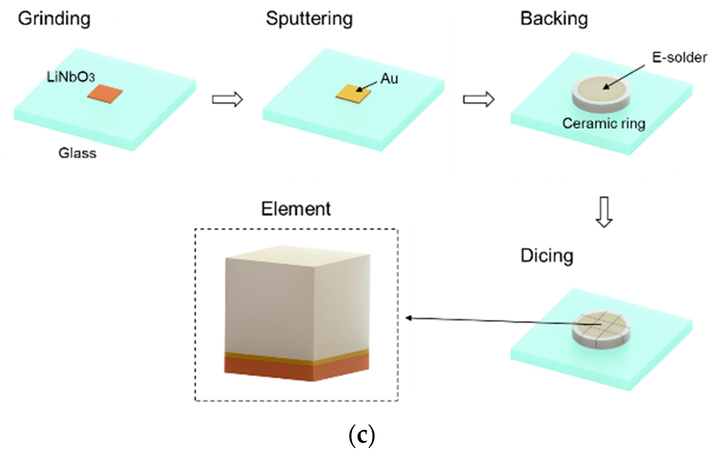
2.2. Fabrication of UHF Ultrasound Transducer
3. Results
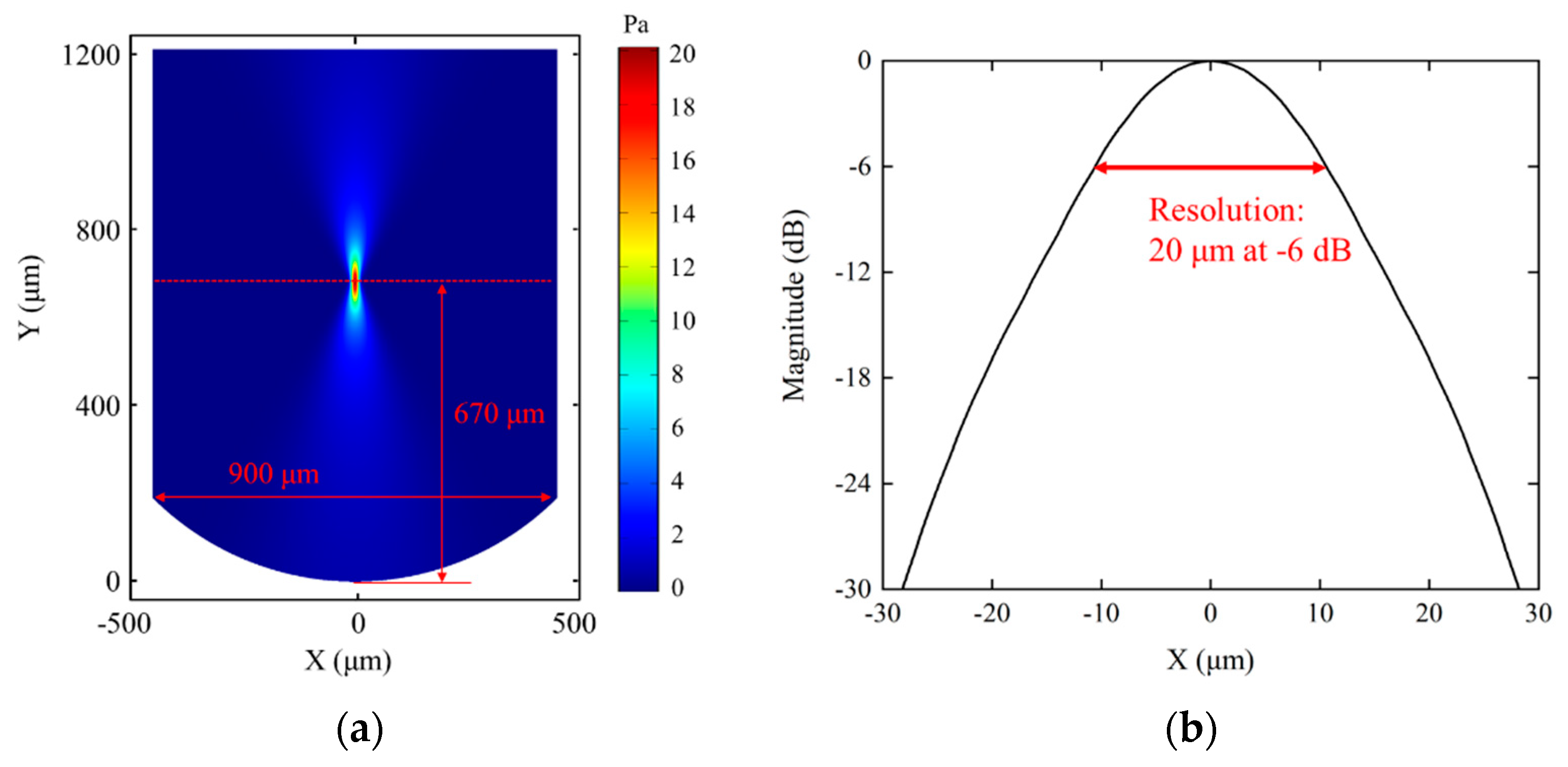
3.1. Characteristics of Transducers
3.2. B-Scan Imaging
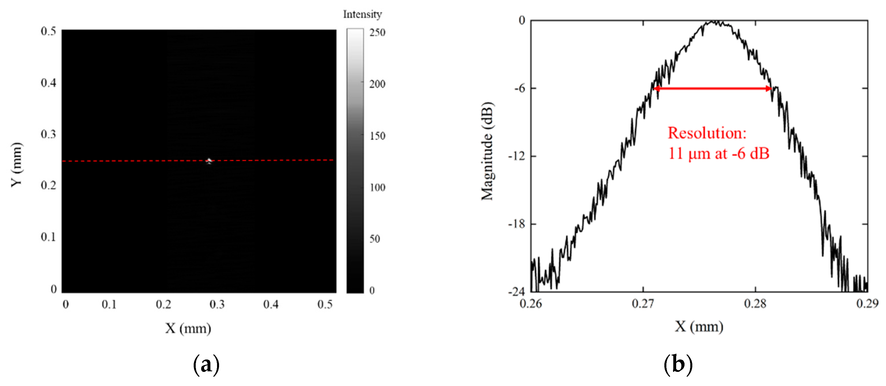
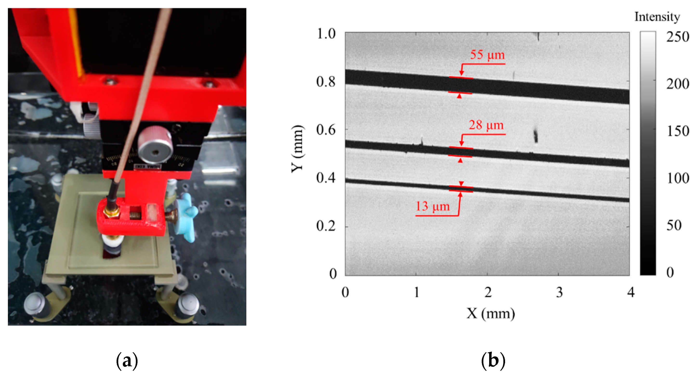
3.3. C-Scan Imaging
4. Discussion
Author Contributions
Funding
Institutional Review Board Statement
Informed Consent Statement
Data Availability Statement
Acknowledgments
Conflicts of Interest
References
- Lemons, R.A.; Quate, C.F. Acoustic microscope-scanning version. Appl. Phys. Lett. 1974, 24, 163–165. [Google Scholar] [CrossRef]
- Ramanathan, S.; Semmens, J.E.; Kessler, L.W. High-frequency acoustic microscopy studies of buried interfaces in silicon. In Proceedings of the 56th Electronic Components and Technology Conference, San Diego, CA, USA, 30 May–2 June 2006. [Google Scholar] [CrossRef]
- Jakob, A.; Weiss, E.C.; Knoll, T.; Bauerfeld, F.; Hermann, J.; Lemor, R. P2E-5 Silicon Based GHz Acoustic Lenses For Time Resolved Acoustic Microscopy. In Proceedings of the 2007 IEEE Ultrasonics Symposium Proceedings, New York, NY, USA, 28–31 October 2007; pp. 1605–1608. [Google Scholar] [CrossRef]
- Weiss, E.C.; Anastasiadis, P.; Pilarczyk, G.; Lemor, R.M.; Zinin, P.V. Mechanical properties of single cells by high-frequency time-resolved acoustic microscopy. IEEE T. Ultrason. Ferr. 2007, 54, 2257–2271. [Google Scholar] [CrossRef] [PubMed]
- Rohrbach, D.; Jakob, A.; Lloyd, H.O.; Tretbar, S.H.; Silverman, R.H.; Mamou, J. A Novel Quantitative 500-MHz Acoustic Microscopy System for Ophthalmologic Tissues. IEEE T. Bio-Med. Eng. 2017, 64, 715–724. [Google Scholar] [CrossRef] [PubMed] [Green Version]
- Jakob, A.; Bender, M.; Knoll, T.; Lemor, R.; Lehnert, T.; Koch, M.; Veith, M.; Zhou, Q.; Zhu, B.P.; Han, J.X.; et al. Comparison of different piezoelectric materials for GHz acoustic microscopy transducers. In Proceedings of the 2009 IEEE International Ultrasonics Symposium, Rome, Italy, 20–23 September 2009; pp. 1722–1725. [Google Scholar] [CrossRef]
- Xu, Z.Y.; Gao, S.Y.; Huang, J.; Wang, Y. Non-Destructive Testing of Polycrystalline Silicon Solar Panel by Scan Acoustic Microscopy. Adv. Mat. Res. 2013, 764, 9–13. [Google Scholar] [CrossRef]
- Brand, S.; Appenroth, T.; Naumann, F.; Steller, W.; Wolf, M.J.; Czurratis, P.; Altmann, F.; Petzold, M. Acoustic GHz-microscopy and its potential applications in 3D-integration technologies. In Proceedings of the IEEE 65th Electronic Components and Technology Conference, San Diego, CA, USA, 26–29 May 2015. [Google Scholar] [CrossRef]
- Brand, S.; Altmann, F. Lock-in-thermography, photoemission, and time-resolved GHz acoustic microscopy techniques for nondestructive defect localization in TSV. IEEE Trans. Comp. Packag. Manuf. Technol. 2018, 8, 735–744. [Google Scholar] [CrossRef]
- Fei, C.L.; Chiu, C.T.; Chen, X.Y.; Chen, Z.Y.; Ma, J.G.; Zhu, B.P.; Shung, K.K.; Zhou, Q.F. Ultrahigh frequency (100 MHz-300 MHz) ultrasonic transducers for optical resolution medical imagining. Sci. Rep. 2016, 6, 28360. [Google Scholar] [CrossRef] [PubMed]
- Zhang, T.F.; Chen, R.M.; Zhang, Z.Q.; Li, R.Z.; Tang, X.G.; Wang, X.Q.; Shung, K.K.; Zhou, Q.F. High frequency single crystal ultrasonic transducers up to 100 MHz for high resolution ophthalmic imaging applications. In Proceedings of the 2017 IEEE International Ultrasonics Symposium (IUS), Washington, DC, USA, 6–9 September 2017; pp. 1–4. [Google Scholar] [CrossRef]
- Hildebrand, J.A.; Lam, L.K. Directional acoustic microscopy for observation of elastic anisotropy. Appl. Phys. Lett. 1983, 42, 413–415. [Google Scholar] [CrossRef]
- Canumalla, S. Resolution of broadband transducers in acoustic microscopy of encapsulated ICs: Transducer selection. IEEE Trans. Components Packag. Technol. 1999, 22, 582–592. [Google Scholar] [CrossRef]
- Li, D.; Fei, C.L.; Zhang, Q.D.; Li, Y.N.; Yang, Y.T.; Zhou, Q.F. Ultrahigh Frequency Ultrasonic Transducers Design with Low Noise Amplifier Integrated Circuit. Micromachines 2018, 9, 515. [Google Scholar] [CrossRef] [PubMed] [Green Version]
- Li, Z.; Wang, D.; Fei, C.; Qiu, Z.; Hou, C.; Wu, R.; Li, D.; Zhang, Q.; Chen, D.; Chen, Z.J.I. The forbidden band and size selectivity of acoustic radiation force trapping. iScience 2021, 24, 101988. [Google Scholar] [CrossRef] [PubMed]
- Chen, X.Y.; Lam, K.H.; Chen, R.M.; Chen, Z.Y.; Yu, P.; Chen, Z.P.; Shung, K.K.; Zhou, Q.F. An Adjustable Multi-Scale Single Beam Acoustic Tweezers Based on Ultrahigh Frequency Ultrasonic Transducer. Biotechnol. Bioeng. 2017, 114, 2637–2647. [Google Scholar] [CrossRef] [PubMed]
- Lim, H.G.; Shung, K.K. Quantification of Inter-Erythrocyte Forces with Ultra-High Frequency (410 MHz) Single Beam Acoustic Tweezer. Ann. Biomed. Eng. 2017, 45, 2174–2183. [Google Scholar] [CrossRef] [PubMed]
- Fei, C.L.; Hsu, H.S.; Vafanejad, A.; Li, Y.; Lin, P.F.; Li, D.; Yang, Y.T.; Kim, E.; Shung, K.K.; Zhou, Q.F. Ultrahigh frequency ZnO silicon lens ultrasonic transducer for cell-size microparticle manipulation. J. Alloy. Compd. 2017, 729, 556–562. [Google Scholar] [CrossRef]
- Chou, C.H.; Khuri-Yakub, B.T.; Kino, G.S. Lens design for acoustic microscopy. IEEE Trans. Ultrason. Ferroelectr. Freq. Control 1988, 35, 464–469. [Google Scholar] [CrossRef] [PubMed]
- Bozkurt, A.; Yarahoglu, G.; Atalar, A.; Koymen, H. A new directional acoustic lens: V-groove lens. In Proceedings of the IEEE Ultrasonics Symposium, Baltimore, MD, USA, 31 October–3 November 1993. [Google Scholar] [CrossRef]
- Li, J.; Friedrich, C.R.; Keynton, R.S. Design and fabrication of a miniaturized, integrated, high-frequency acoustical lens–transducer system. J. Micromech. Microeng. 2002, 12, 219–228. [Google Scholar] [CrossRef]
- Hashimoto, H.; Tanaka, S.; Sato, K.; Ishikawa, I.; Kato, S.; Chubachi, N. Chemical isotropic etching of single-crystal silicon for acoustic lens of scanning acoustic microscope. Jpn. J. Appl. Phys. 1993, 32, 2543. [Google Scholar] [CrossRef]
- Briggs, A.; Kolosov, O. Acoustic Microscopy; Oxford university press: Oxford, UK, 2010; Volume 67. [Google Scholar]
- Chen, J.; Dai, J.Y.; Zhang, C.; Zhang, Z.T.; Feng, G.P. Bandwidth improvement of LiNbO3 ultrasonic transducers by half-concaved inversion layer approach. Rev. Sci. Instrum. 2012, 83, 114903. [Google Scholar] [CrossRef] [PubMed] [Green Version]
- Chen, R.; He, Y.; Shi, J.; Yung, C.; Hwang, J.; Wang, L.V.; Zhou, Q. Transparent High-Frequency Ultrasonic Transducer for Photoacoustic Microscopy Application. IEEE T. Ultrason. Ferr. 2020, 67, 1848–1853. [Google Scholar] [CrossRef] [PubMed]
- Lam, K.; Hsu, H.; Li, Y.; Lee, C.; Lin, A.; Zhou, Q.; Kim, E.; Shung, K. Ultrahigh frequency lensless ultrasonic transducers for acoustic tweezers application. Biotechnol. Bioeng. 2013, 110, 881–886. [Google Scholar] [CrossRef] [PubMed] [Green Version]
- Hashimoto, H.; Tanaka, S.; Sato, K. Silicon acoustic lens for scanning acoustic microscope (SAM). In Proceedings of the TRANSDUCERS ‘91: 1991 International Conference on Solid-State Sensors and Actuators, Digest of Technical Papers. San Francisco, CA, USA, 24–27 June 1991; pp. 853–859. [Google Scholar] [CrossRef]


| Size (feet) | Thickness (μm) | Type | Orientation | Resistivity (Ω·cm) | Surface Treatment |
|---|---|---|---|---|---|
| 2 | 500 | N | 100 | 1–10 | single-side polishing, no oxide film |
| Velocity (m/s) | Density (kg/m3) | Acoustic Impedance (MRayl) | |
|---|---|---|---|
| LiNbO3 | 7360 | 4688 | 34.5 |
| Si | 8430 | 2340 | 19.8 |
| E-solder 3022 | 1850 | 3200 | 5.9 |
| Water | 1540 | 1000 | 1.5 |
| Center Frequecy (MHz) | −6-dB Bandwidth (%) | Pulse Duration (ns) | Focal Distance (μm) | |
|---|---|---|---|---|
| Silicon lens Transducer | 157 | 52 | 8 | 736 |
| Method | Cost | Time | Complexity | Difficulty |
|---|---|---|---|---|
| Ultraprecision machining | Low | Short | Single step | Easy |
| Etching | High | Long | A series of steps | Hard |
Disclaimer/Publisher’s Note: The statements, opinions and data contained in all publications are solely those of the individual author(s) and contributor(s) and not of MDPI and/or the editor(s). MDPI and/or the editor(s) disclaim responsibility for any injury to people or property resulting from any ideas, methods, instructions or products referred to in the content. |
© 2023 by the authors. Licensee MDPI, Basel, Switzerland. This article is an open access article distributed under the terms and conditions of the Creative Commons Attribution (CC BY) license (https://creativecommons.org/licenses/by/4.0/).
Share and Cite
Chen, J.; Fei, C.; Zhao, J.; Quan, Y.; Wang, Y.; Jiang, Z.; Wen, L. Ultrahigh Frequency Ultrasonic Transducers (150MHz) Based on Silicon Lenses. Micromachines 2023, 14, 213. https://doi.org/10.3390/mi14010213
Chen J, Fei C, Zhao J, Quan Y, Wang Y, Jiang Z, Wen L. Ultrahigh Frequency Ultrasonic Transducers (150MHz) Based on Silicon Lenses. Micromachines. 2023; 14(1):213. https://doi.org/10.3390/mi14010213
Chicago/Turabian StyleChen, Jun, Chunlong Fei, Jianxin Zhao, Yi Quan, Yecheng Wang, Zhishui Jiang, and Li Wen. 2023. "Ultrahigh Frequency Ultrasonic Transducers (150MHz) Based on Silicon Lenses" Micromachines 14, no. 1: 213. https://doi.org/10.3390/mi14010213