
High-Efficiency Copper Removal by Nitrogen Plasma-Assisted Picosecond Laser Processing

Abstract
:1. Introduction
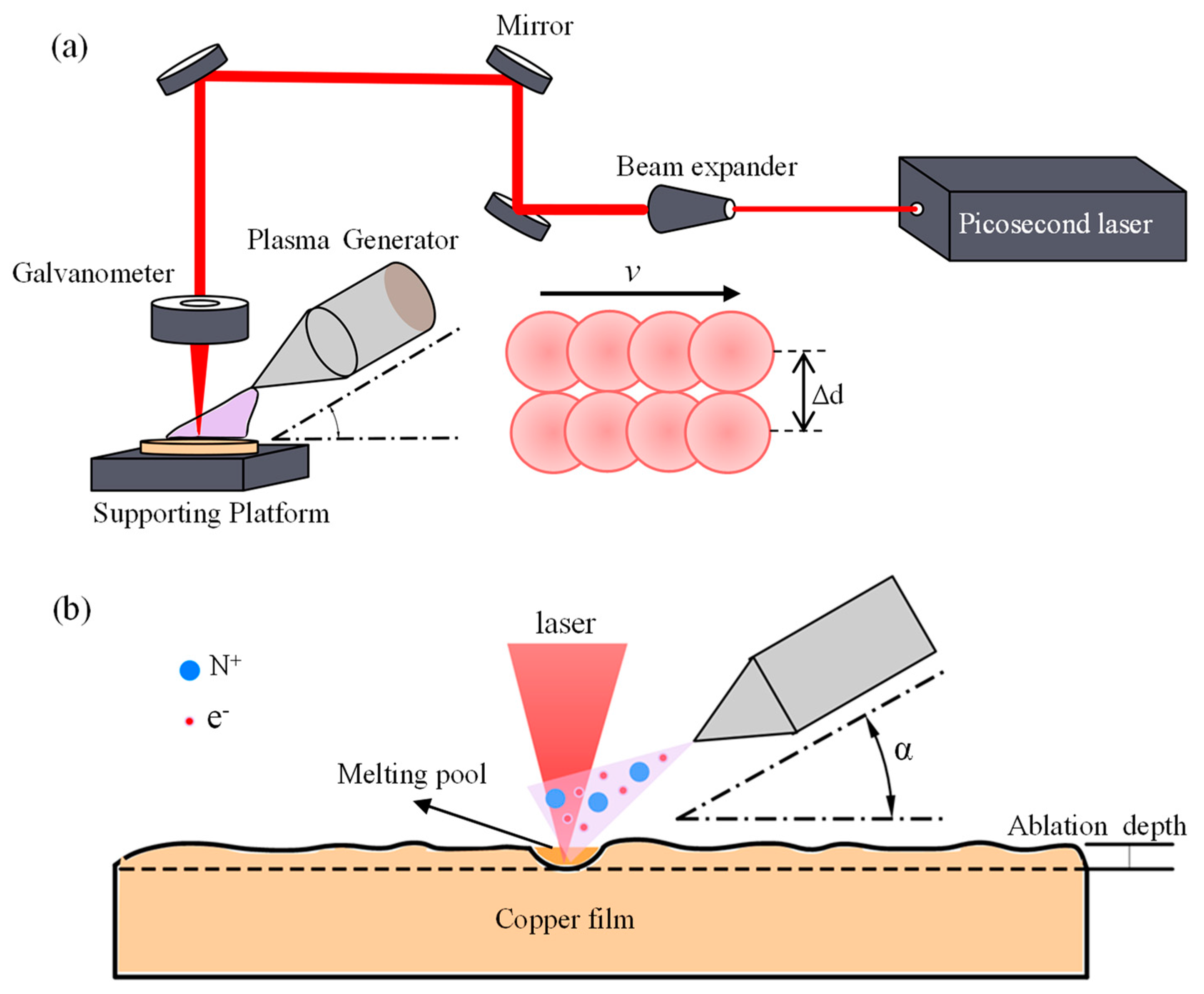
2. Experiment
2.1. Materials
2.2. Experimental Process
2.3. Characterization
3. Theoretical Analysis and Simulation
3.1. Mechanism Analysis
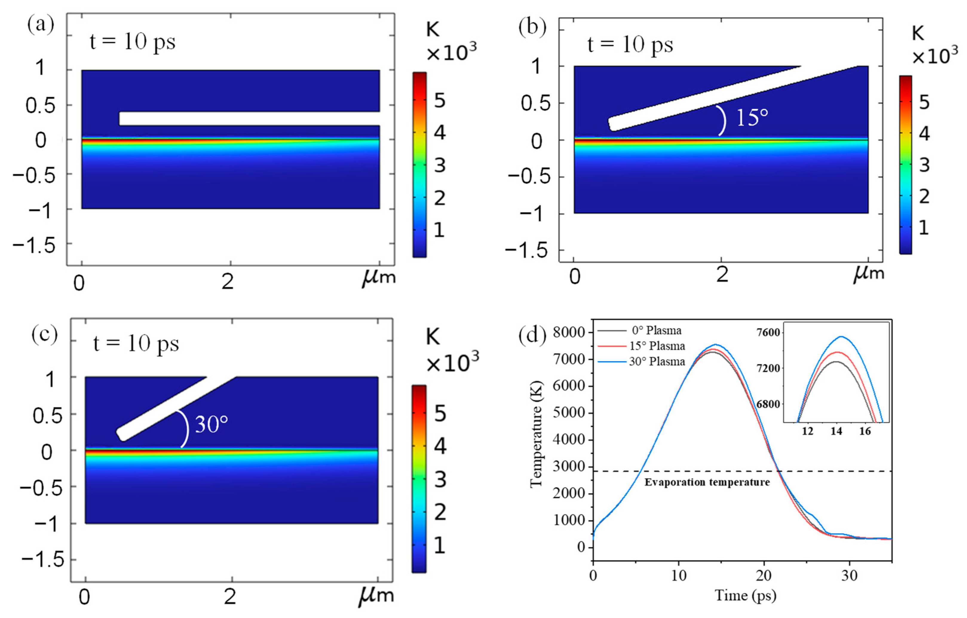
3.2. Numerical Model
4. Results and Discussion
4.1. Simulation Results
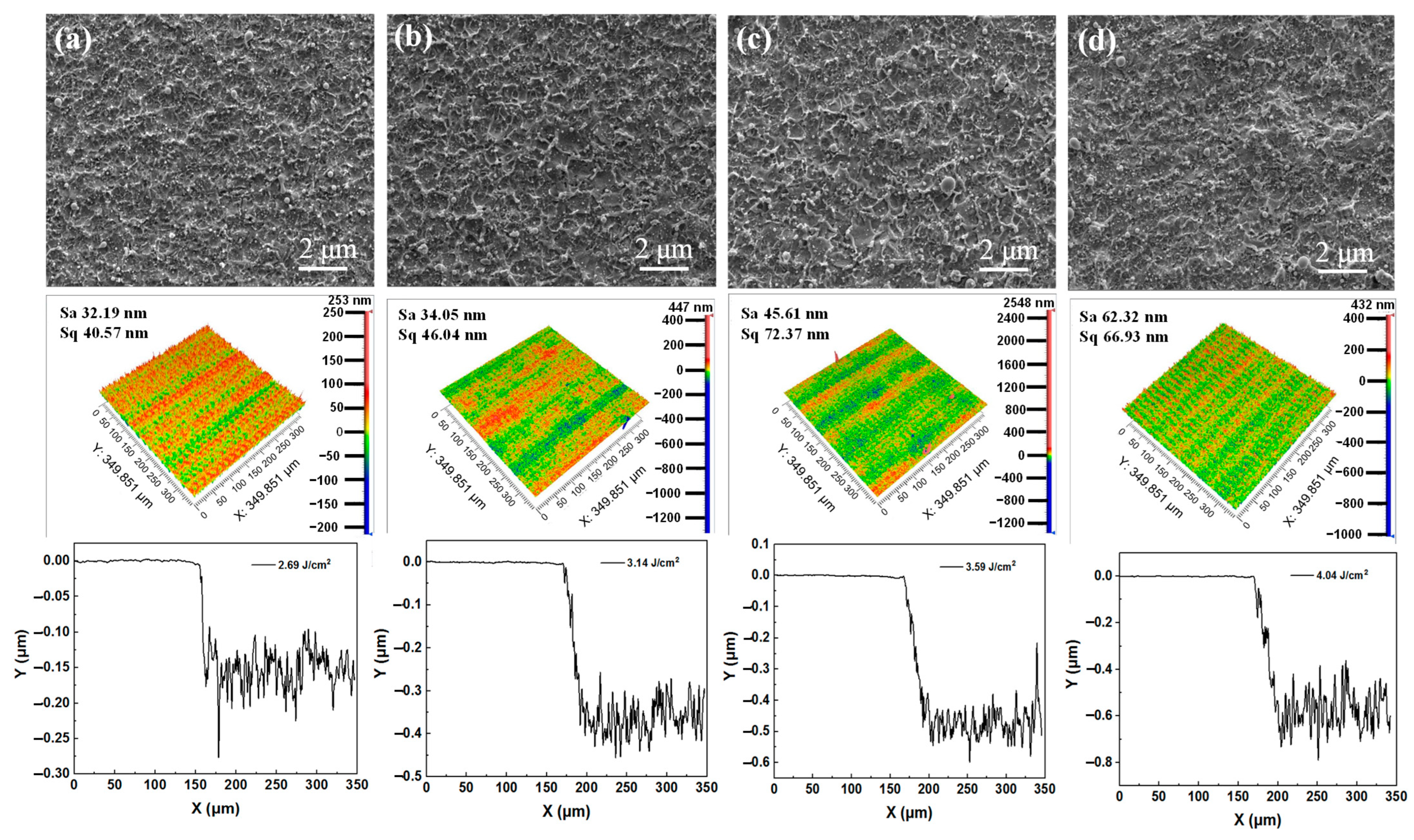
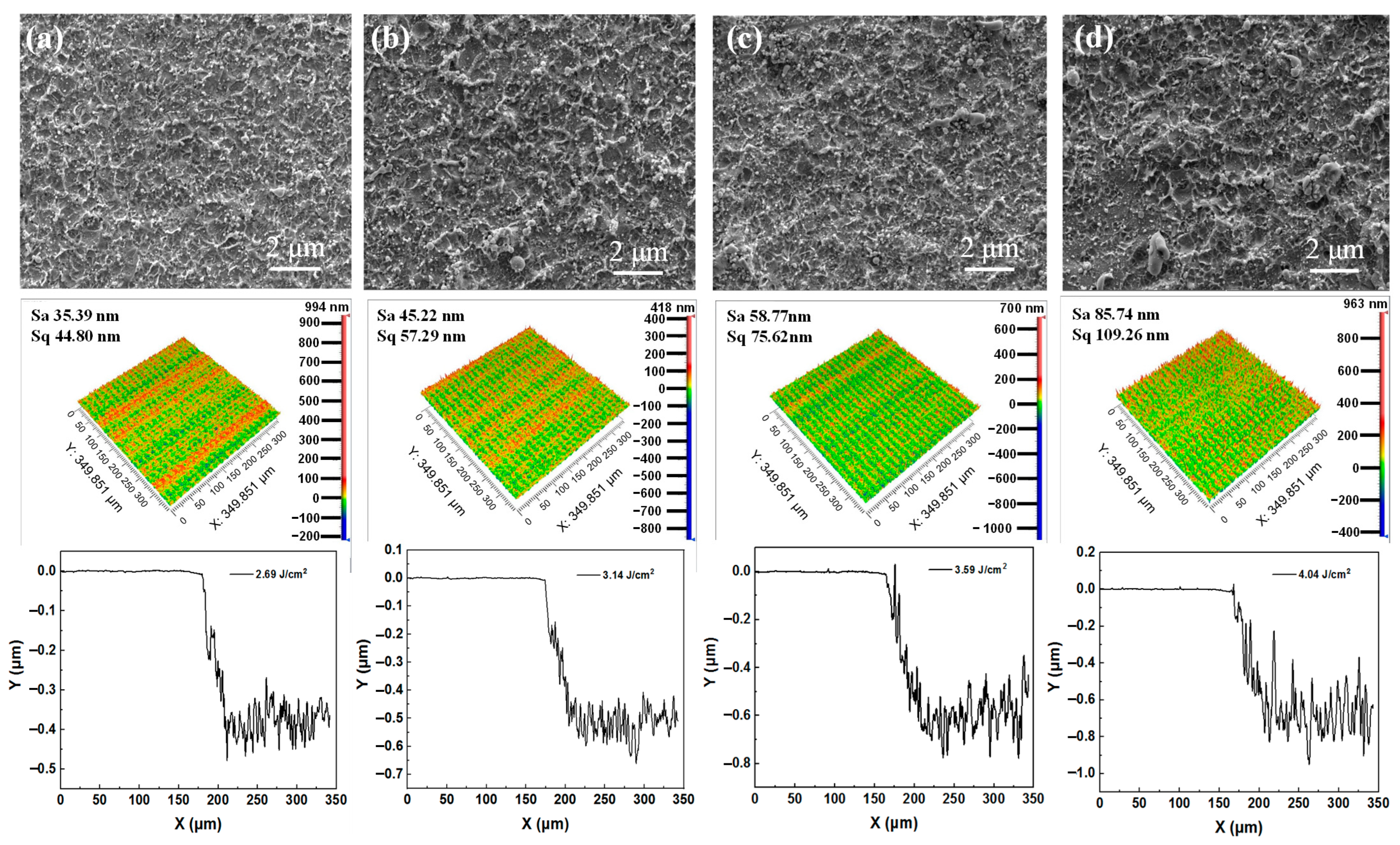
4.2. Cu Removal by PS-Laser without Plasma Assistance
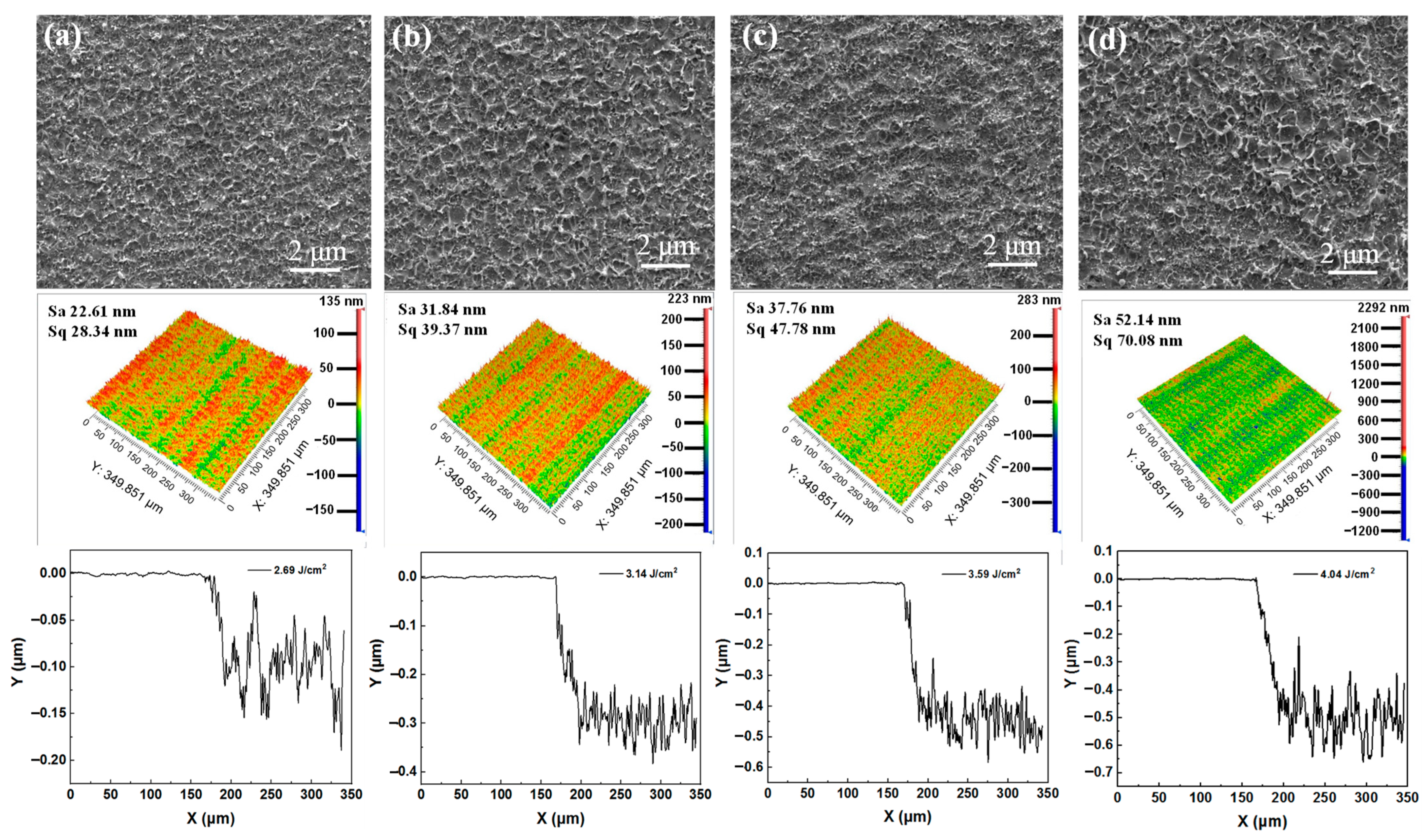
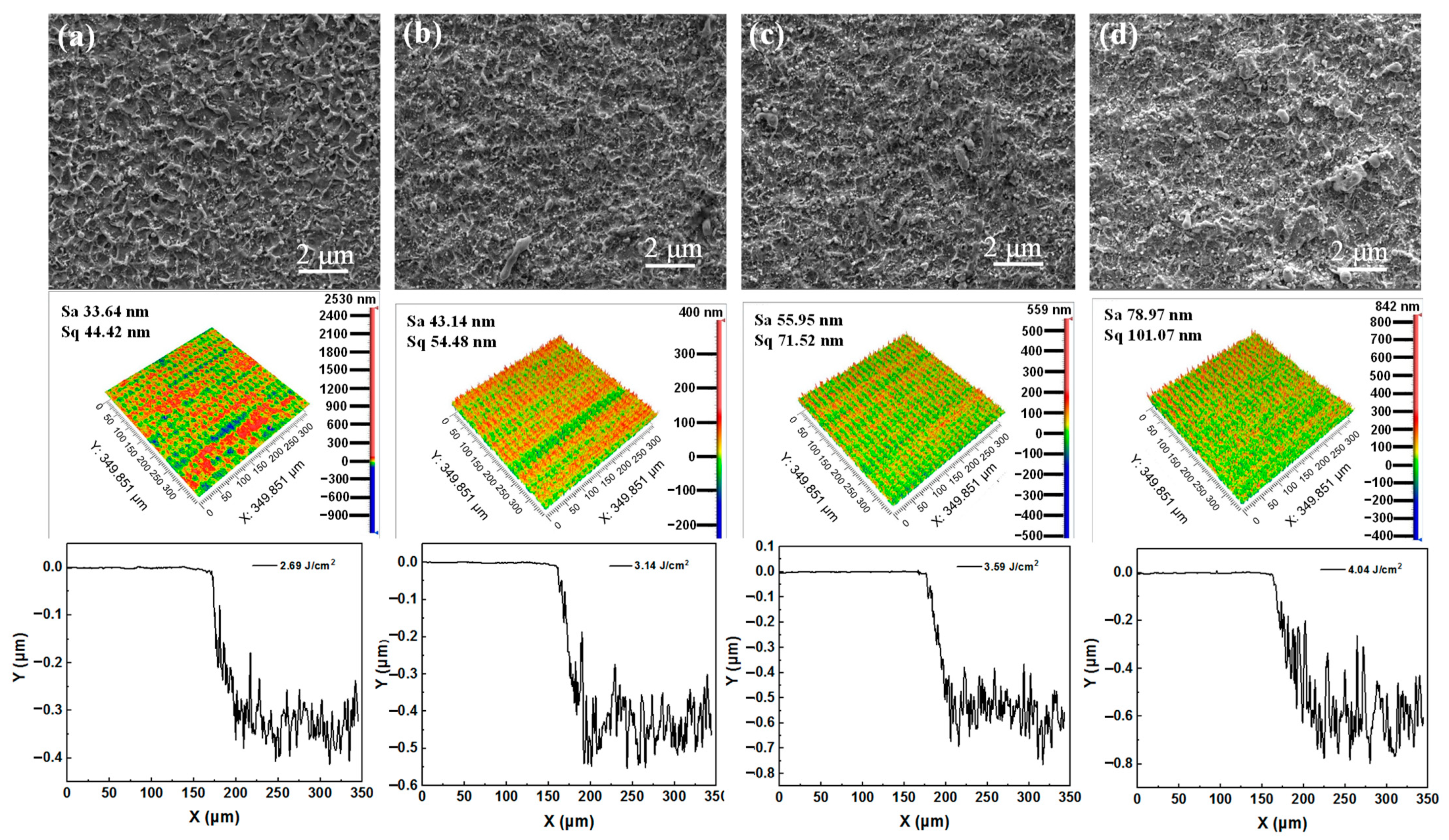
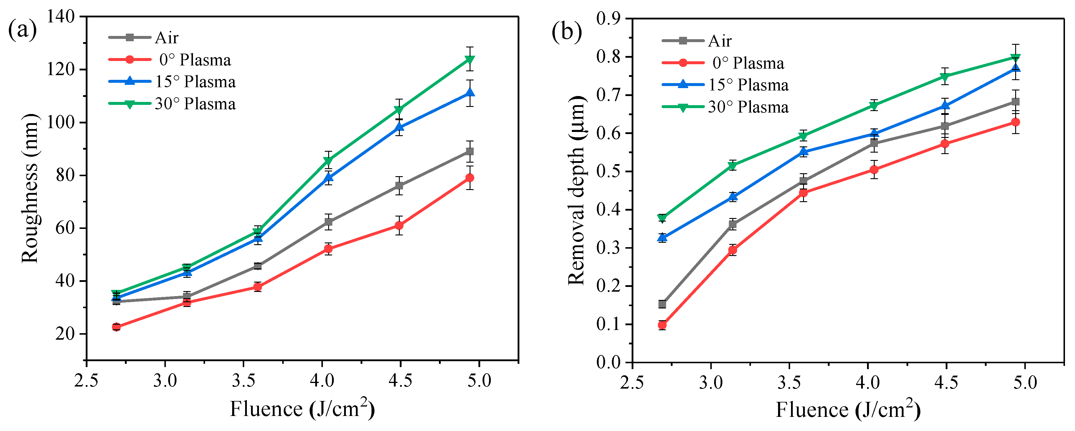
4.3. Cu Removal by PS-Laser with Plasma Assistance
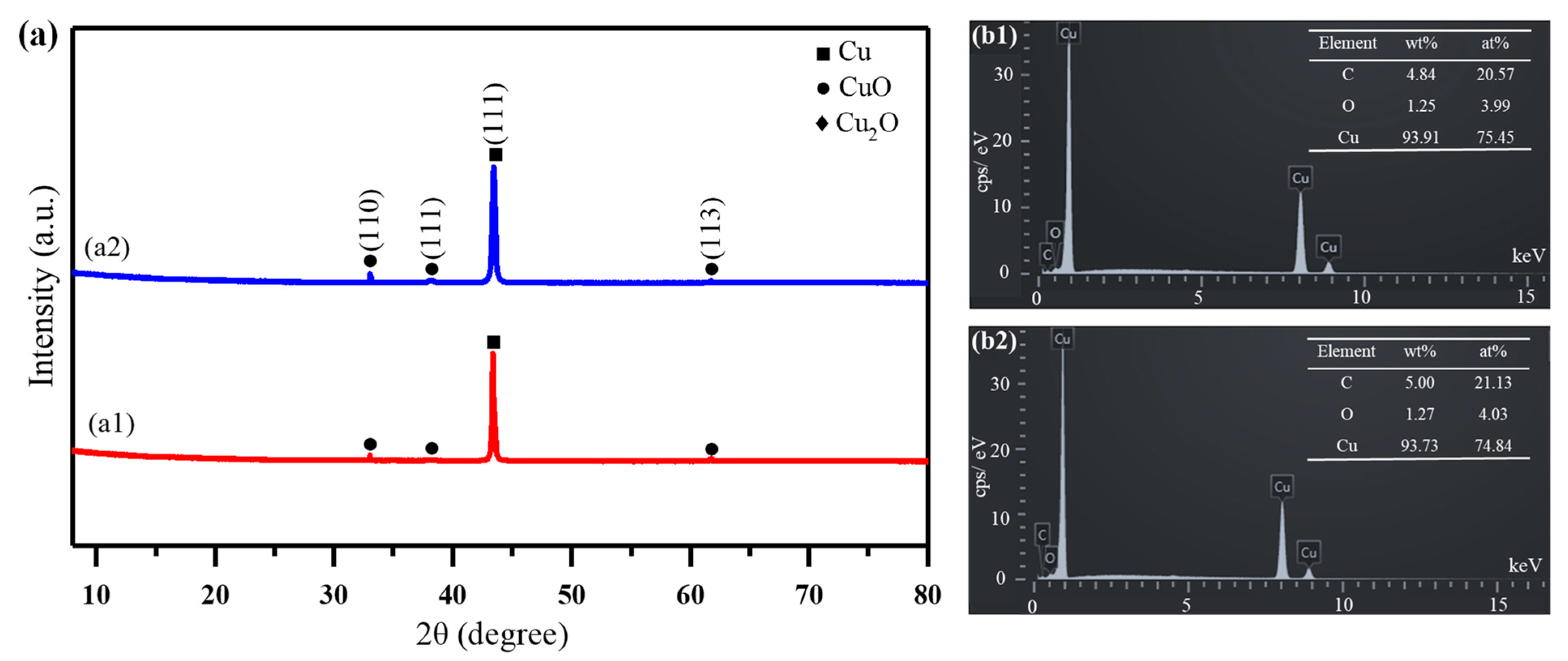
4.4. Analysis of the Processed Cu Films
5. Conclusions
Author Contributions
Funding
Data Availability Statement
Conflicts of Interest
References
- Shi, S.; Wang, X.; Xu, C.; Yuan, J.; Fang, J.; Liu, S. Simulation and fabrication of two Cu TSV electroplating methods for wafer-level 3D integrated circuits packaging. Sens. Actuator A Phys. 2013, 203, 52–61. [Google Scholar] [CrossRef]
- Li, Z.; Khuje, S.; Chivate, A.; Huang, Y.; Hu, Y.; An, L.; Shao, Z.; Wang, J.; Chang, S.; Ren, S. Printable copper sensor electronics for high temperature. ACS Appl. Electron. Mater. 2020, 2, 1867–1873. [Google Scholar] [CrossRef]
- Politis, D.J.; Lin, J.; Dean, T.A.; Balint, D.S. An investigation into the forging of Bi-metal gears. J. Mater. Process. Technol. 2014, 214, 2248–2260. [Google Scholar] [CrossRef]
- Arai, S.; Hasegawa, T.; Kaneko, N. Fabrication of three-dimensional Cu/Ni multilayered microstructure by wet process. Electrochim. Acta 2004, 49, 945–950. [Google Scholar] [CrossRef]
- Khan, R.; Misran, M.A.B.; Ohtaki, M.; Song, J.T.; Ishihara, T.; Hattori, R. Back-Channel Etched In-Ga-Zn-O Thin-Film Transistor Utilizing Selective Wet-Etching of Copper Source and Drain. Processes 2021, 9, 2193. [Google Scholar] [CrossRef]
- Kim, J.K.; Choi, Y.S.; Lee, D.W. Surface-adaptable all-metal micro-four-point probe with unique configuration. J. Micromechanics Microengineering 2015, 25, 75023–75028. [Google Scholar] [CrossRef]
- Liu, J.; Zhang, Y.; Shan, H.; Qi, L.; Tang, H.; Guo, H.; Liu, Z.; Hu, X.; Xu, Z.; Liu, C. Sacrificial layer-assisted one-step transfer printing for fabricating a three-layer dry electrode. Sens. Actuators A Phys. 2020, 306, 111954. [Google Scholar] [CrossRef]
- Yang, Y.; Liu, J.; Zheng, J.; Lu, M.; Shi, J.; Hong, W.; Yang, F.; Tian, Z. Promising electroplating solution for facile fabrication of Cu quantum point contacts. Nano Res. 2017, 10, 3314–3323. [Google Scholar] [CrossRef]
- Yuan, Z.; Chen, Y.; Ni, Z.; Wang, Y.; Yi, H.; Li, T. Wafer-level site-controlled growth of silicon nanowires by Cu pattern dewetting. Nano Res. 2015, 8, 2646–2653. [Google Scholar] [CrossRef]
- Lee, J.; Park, C.; Kim, H. Sheet resistance variation of graphene grown on annealed and mechanically polished Cu films. RSC Adv. 2014, 4, 62453–62456. [Google Scholar] [CrossRef]
- Yun, S.; Son, Y.; Jeong, G.; Lee, J.; Jeong, J.; Bae, J.; Kim, S.; Park, J.; Park, J. Dishing-free chemical mechanical planarization for copper films. Colloids Surf. A 2021, 616, 126143. [Google Scholar] [CrossRef]
- Zhang, L.; Wang, T.; Lu, X. Potassium persulfate as an oxidizer in chemical mechanical polishing slurries relevant for copper interconnects with cobalt barrier layers. J. Mater. Sci. 2020, 55, 8992–9002. [Google Scholar] [CrossRef]
- Zhang, Z.; Cui, J.; Zhang, J.; Liu, D.; Yu, Z.; Guo, D. Environment friendly chemical mechanical polishing of copper. Appl. Surf. Sci. 2019, 467–468, 5–11. [Google Scholar] [CrossRef]
- Zhong-yu, P.; Dong-hui, W.; Lin-zhi, Y.; Meng-meng, Z. Ultra-smooth Cu surface fabricated by hydrodynamic suspension polishing technique. Precis. Eng. 2019, 57, 189–194. [Google Scholar] [CrossRef]
- Zhou, J.; Niu, X.; Yang, C.; Huo, Z.; Lu, Y.; Wang, Z.; Cui, Y.; Wang, R. Surface action mechanism and planarization effect of sarcosine as an auxiliary complexing agent in copper film chemical mechanical polishing. Appl. Surf. Sci. 2020, 529, 147109. [Google Scholar] [CrossRef]
- Hu, H.; Chen, K. Development of low temperature Cu-Cu bonding and hybrid bonding for three-dimensional integrated circuits (3D IC). Microelectron. Reliab. 2021, 127, 114412. [Google Scholar] [CrossRef]
- Huang, Z.; Jones, R.E.; Jain, A. Experimental investigation of electromigration failure in Cu–Sn–Cu micropads in 3D integrated circuits. Microelectron. Eng. 2014, 122, 46–51. [Google Scholar] [CrossRef]
- Made, R.I.; Lan, P.; Li, H.Y.; Gan, C.L.; Tan, C.S. Effect of direct current stressing to Cu–Cu bond interface imperfection for three dimensional integrated circuits. Microelectron. Eng. 2013, 106, 149–154. [Google Scholar] [CrossRef]
- Tian, T.; Morusupalli, R.; Shin, H.; Son, H.Y.; Byun, K.Y.; Joo, Y.C.; Caramto, R.; Smith, L.; Shen, Y.; Kunz, M.; et al. On the mechanical stresses of Cu through-silicon via (TSV) samples fabricated by SK Hynix vs. SEMATECH—enabling robust and reliable 3-D interconnect/integrated circuit (IC) technology. Procedia Eng. 2016, 139, 101–111. [Google Scholar] [CrossRef]
- Hong, S.; Han, D.; Kwon, J.; Kim, S.J.; Lee, S.J.; Jang, K. Influence of abrasive morphology and size dispersity of Cu barrier metal slurry on removal rates and wafer surface quality in chemical mechanical planarization. Microelectron. Eng. 2020, 232, 111417. [Google Scholar] [CrossRef]
- Xu, R.; Wang, Y.; Wang, Y.; Lui, H.; Su, J. Study on oxidant in chemical mechanical polishing of copper. Trans. Electr. Electron. Mater. 2020, 21, 580–586. [Google Scholar] [CrossRef]
- Wang, K.; Yan, Y.; Zhou, P.; Shi, K.; Guo, D. Effect of cupric ion concentration on the etching behavior of copper in Electrogenerated Chemical Polishing (EGCP). Precis. Eng. 2019, 55, 70–76. [Google Scholar] [CrossRef]
- Yang, L.; Liu, Y.; Wang, C.; Tan, B.; Gao, B.; Han, C.; Liu, Y.; Tang, X. Role of penetrating agent on colloidal silica particle removal during post Cu CMP Cleaning. ECS J. Solid State Sci. 2018, 7, P380–P384. [Google Scholar] [CrossRef]
- Huang, Y.; Xie, X.; Cui, J.; Zhou, W.; Chen, J.; Long, J. Robust metallic micropatterns fabricated on quartz glass surfaces by femtosecond laser-induced selective metallization. Opt. Express 2022, 30, 19544–19556. [Google Scholar] [CrossRef]
- Wang, T.; Zhu, H.; Zhang, Z.; Gao, J.; Wu, Y.; Hu, M.; Xu, K. Preparing of superamphiphobic surface by fabricating hierarchical nano re-entrant pyramids on micro-cones using a combined laser-electrochemistry method. Surf. Interfaces 2021, 24, 101112. [Google Scholar] [CrossRef]
- Kwon, M.H.; Shin, H.S.; Chu, C.N. Fabrication of a super-hydrophobic surface on metal using laser ablation and electrodeposition. Appl. Surf. Sci. 2014, 288, 222–228. [Google Scholar] [CrossRef]
- Trtica, M.; Limpouch, J.; Stasic, J.; Gavrilov, P. Femtosecond laser-assisted surface modification of tungsten with 1015 W/cm2 intensity in air and vacuum ambience. Appl. Surf. Sci. 2019, 464, 99–107. [Google Scholar] [CrossRef]
- Zhang, Z.; Gu, Q.; Jiang, W.; Zhu, H.; Xu, K.; Ren, Y.; Xu, C. Achieving of bionic super-hydrophobicity by electrodepositing nano-Ni-pyramids on the picosecond laser-ablated micro-Cu-cone surface. Surf. Coat. Technol. 2019, 363, 170–178. [Google Scholar] [CrossRef]
- Gu, Y.; Dong, C.; Zhong, M.; Ma, M.; Li, L.; Liu, W. Fabrication of nanoporous manganese by laser cladding and selective electrochemical de-alloying. Appl. Surf. Sci. 2011, 257, 3211–3215. [Google Scholar] [CrossRef]
- Han, S.; Hong, S.; Yeo, J.; Kim, D.; Kang, B.; Yang, M.; Ko, S.H. Nanorecycling: Monolithic integration of copper and copper oxide nanowire network electrode through selective reversible photothermochemical reduction. Adv. Mater. 2015, 27, 6397–6403. [Google Scholar] [CrossRef]
- Oboňa, J.V.; Ocelík, V.; Rao, J.C.; Skolski, J.Z.; Römer, G.R.; Huis, A.J.; De Hosson, J.T. Modification of Cu surface with picosecond laser pulses. Appl. Surf. Sci. 2014, 303, 118–124. [Google Scholar] [CrossRef]
- Fikry, M.; Tawfik, W.; Omar, M. Measurement of the electron temperature in a metallic copper using ultrafast laser-induced breakdown spectroscopy. J. Russ. Laser Res. 2020, 41, 484–490. [Google Scholar] [CrossRef]
- Fikry, M.; Tawfik, W.; Omar, M. Controlling the plasma electron number density of copper metal using NIR picosecond laser-induced plasma spectroscopy. Opt. Appl. 2021, 51, 365–374. [Google Scholar] [CrossRef]
- Fikry, M.; Tawfik, W.; Omar, M.M. Investigation on the effects of laser parameters on the plasma profile of copper using picosecond laser induced plasma spectroscopy. Opt. Quantum Electron. 2020, 52, 249. [Google Scholar] [CrossRef]
- Schille, J.; Schneider, L.; Loeschner, U. Process Optimization in high-average-power ultrashort pulse laser microfabrication: How laser process parameters influence efficiency, throughput and quality. Appl. Phys. A 2015, 120, 847–855. [Google Scholar] [CrossRef]
- Gerhard, C.; Dammann, M.; Wieneke, S.; Viöl, W. Sequential atmospheric pressure plasma-assisted laser ablation of photovoltaic cover glass for improved contour accuracy. Micromachines 2014, 5, 408–419. [Google Scholar] [CrossRef]
- Kim, B.; Nam, H.K.; Watanabe, S.; Park, S.; Kim, Y.; Kim, Y.; Fushinobu, K.; Kim, S. Selective laser ablation of metal thin films using ultrashort pulses. Int. J. Precis. Eng. Manuf.-Green Technol. 2021, 8, 771–782. [Google Scholar] [CrossRef]
- Li, Y.; Guo, X.; Wang, S.; Zhao, Y.; Zhang, C.; Liu, S.; Cheng, G.J.; Liu, F. High-precision and high-efficiency copper removal by femtosecond laser in mixed hydrochloric acid-oxygen atmosphere. J. Manuf. Process. 2022, 82, 152–158. [Google Scholar] [CrossRef]
- Wang, S.; Wang, Y.; Zhang, S.; Wang, L.; Chen, S.; Zheng, H.; Zhang, C.; Liu, S.; Cheng, G.J.; Liu, F. Nanoscale-precision removal of copper in integrated circuits based on a hybrid process of plasma oxidation and femtosecond laser ablation. Micromachines 2021, 12, 1188. [Google Scholar] [CrossRef]
- Gu, R.; Yao, X.; Wang, D.; Wang, H.; Yan, M.; Wong, K.S. Selective laser melting of Cu–10Sn–0.4P: Processing, microstructure, properties, and brief comparison with additively manufactured Cu–10Sn. Adv. Eng. Mater. 2022, 24, 2100716. [Google Scholar] [CrossRef]
- Kmetec, B.; Kovačič, D.; Možina, J.; Podobnik, B. High-speed energy efficient selective removal of large area copper layer by laser induced delamination. Appl. Surf. Sci. 2009, 255, 8598–8602. [Google Scholar] [CrossRef]
- Li, S.; Wang, Y.; Li, B.; Huang, L.; Ren, N. Femtosecond laser selective ablation of Cu/Ag double-layer metal films for fabricating high-performance mesh-type transparent conductive electrodes and heaters. Opt. Commun. 2021, 483, 126661. [Google Scholar] [CrossRef]
- Meng, X.; Zhang, K.; Guo, X.; Wang, C.; Sun, L. Preparation of micro-textures on cemented carbide substrate surface by plasma-assisted laser machining to enhance the PVD tool coatings adhesion. J. Mater. Process. Technol. 2021, 288, 116870. [Google Scholar] [CrossRef]
- Tang, H.; Qiu, P.; Cao, R.; Zhuang, J.; Xu, S. Repulsive magnetic field-assisted laser-induced plasma micromachining for high-quality microfabrication. Int. J. Adv. Manuf. Technol. 2019, 102, 2223–2229. [Google Scholar] [CrossRef]
- Grottker, S.; Viol, W.; Gerhard, C. Impact of assisting atmospheric pressure plasma on the formation of micro- and nanoparticles during picosecond-laser ablation of titanium. Appl. Opt. 2017, 56, 3365–3371. [Google Scholar] [CrossRef] [PubMed]
- Chen, L.; Zhang, X.; Wang, Y.; Osswald, T.A. Laser polishing of Cu/PLA composite parts fabricated by fused deposition modeling: Analysis of surface finish and mechanical properties. Polym. Compos. 2020, 41, 1356–1368. [Google Scholar] [CrossRef]
- Wang, S.; Wang, L.; Zhang, S.; Zheng, H.; Zhang, C.; Liu, S.; Liu, F.; Cheng, G.J. A low-damage copper removal process by femtosecond laser for integrated circuits. Vacuum 2022, 203, 111273. [Google Scholar] [CrossRef]
- Peng, G.; Chen, J.; Lu, L.; Miao, X.; Dong, Z.; Leng, D. Dual dynamic airflow protection for the removal of fused silica micron particles in the final optics assembly. Aerosol Sci. Technol. 2020, 54, 342–352. [Google Scholar] [CrossRef]
- Wu, S.K.; Zheng, K.; Zou, J.L.; Jiang, F.; Han, X.H. A study of the behavior and effects of nitrogen take-up from protective gas shielding in laser welding of stainless steel. J. Manuf. Process. 2018, 34, 477–485. [Google Scholar] [CrossRef]
- Brückner, S. Hybrid Laser-plasma micro-structuring of fused silica based on surface reduction by a low-temperature atmospheric pressure plasma. J. Laser Micro Nanoeng. 2012, 7, 73–76. [Google Scholar] [CrossRef]
- Gerhard, C.; Weihs, T.; Tasche, D.; Brückner, S.; Wieneke, S.; Viöl, W. Atmospheric pressure plasma treatment of fused silica, related surface and near-surface effects and applications. Plasma Chem. Plasma Process. 2013, 33, 895–905. [Google Scholar] [CrossRef]
- Cai, X.; Ji, C.; Li, C.; Tian, Z.; Wang, X.; Lei, C.; Liu, S. Multiphoton absorption simulation of sapphire substrate under the action of femtosecond laser for larger density of pattern-related process windows. Micromachines 2021, 12, 1571. [Google Scholar] [CrossRef] [PubMed]
- Feng, T.; Chen, G.; Han, H.; Qiao, J. Femtosecond-Laser-Ablation Dynamics in Silicon Revealed by Transient Reflectivity Change. Micromachines 2022, 13, 14. [Google Scholar] [CrossRef] [PubMed]
- Terragni, J.; Miotello, A. Laser ablation of aluminum near the critical regime: A computational gas-dynamical model with temperature-dependent physical parameters. Micromachines 2021, 12, 300. [Google Scholar] [CrossRef]
- Abbasi, N.; Razfar, M.R.; Rezaei, S.M.; Madanipour, K.; Khajehzadeh, M. Experimental investigation of deep-hole micro-drilling of glass using LIPAA process. Mater. Manuf. Process. 2022, 37, 701–711. [Google Scholar] [CrossRef]
- Wang, W.; Sun, L.; Zhang, P.; Qi, L.; Zheng, L.; Dong, W. Microanalysis of molybdenum-copper stainless steel samples by picosecond laser-induced breakdown spectroscopy. Microchem. J. 2020, 158, 105267. [Google Scholar] [CrossRef]


Publisher’s Note: MDPI stays neutral with regard to jurisdictional claims in published maps and institutional affiliations. |
© 2022 by the authors. Licensee MDPI, Basel, Switzerland. This article is an open access article distributed under the terms and conditions of the Creative Commons Attribution (CC BY) license (https://creativecommons.org/licenses/by/4.0/).
Share and Cite
Li, Y.; Guo, X.; Wang, S.; Zhang, S.; Zhao, Y.; Guo, D.; Zhang, C.; Liu, S.; Cheng, G.J.; Liu, F. High-Efficiency Copper Removal by Nitrogen Plasma-Assisted Picosecond Laser Processing. Micromachines 2022, 13, 1492. https://doi.org/10.3390/mi13091492
Li Y, Guo X, Wang S, Zhang S, Zhao Y, Guo D, Zhang C, Liu S, Cheng GJ, Liu F. High-Efficiency Copper Removal by Nitrogen Plasma-Assisted Picosecond Laser Processing. Micromachines. 2022; 13(9):1492. https://doi.org/10.3390/mi13091492
Chicago/Turabian StyleLi, Yunfan, Xuanqi Guo, Shuai Wang, Shizhuo Zhang, Yilin Zhao, Dingyi Guo, Chen Zhang, Sheng Liu, Gary J. Cheng, and Feng Liu. 2022. "High-Efficiency Copper Removal by Nitrogen Plasma-Assisted Picosecond Laser Processing" Micromachines 13, no. 9: 1492. https://doi.org/10.3390/mi13091492