
Design of Power/Ground Noise Suppression Structures Based on a Dispersion Analysis for Packages and Interposers with Low-Loss Substrates

Abstract
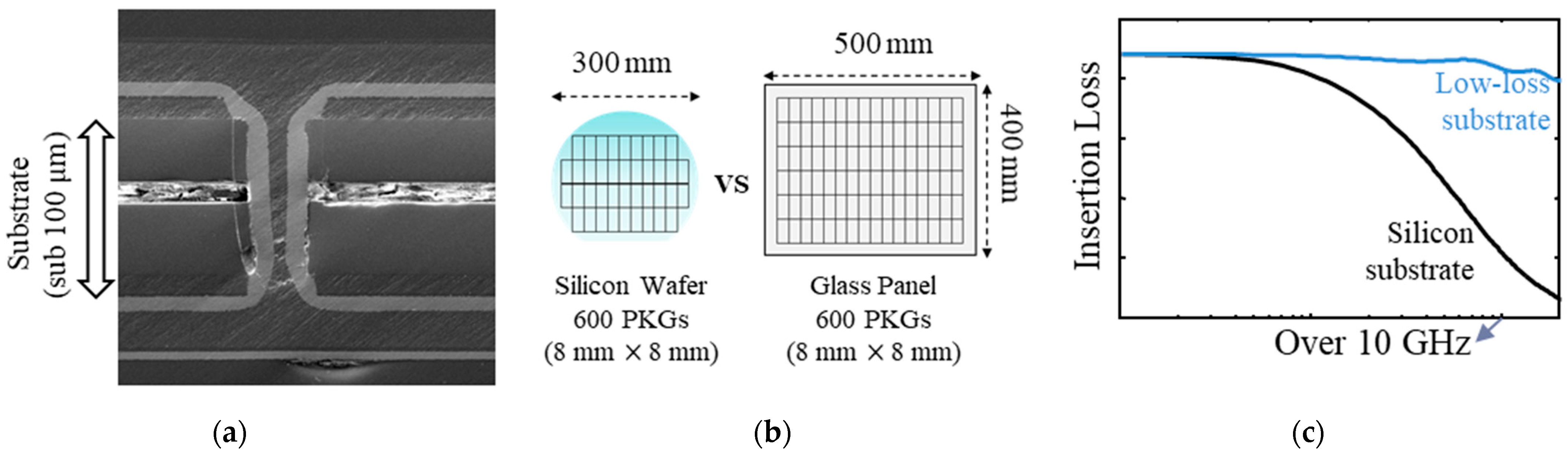
:1. Introduction
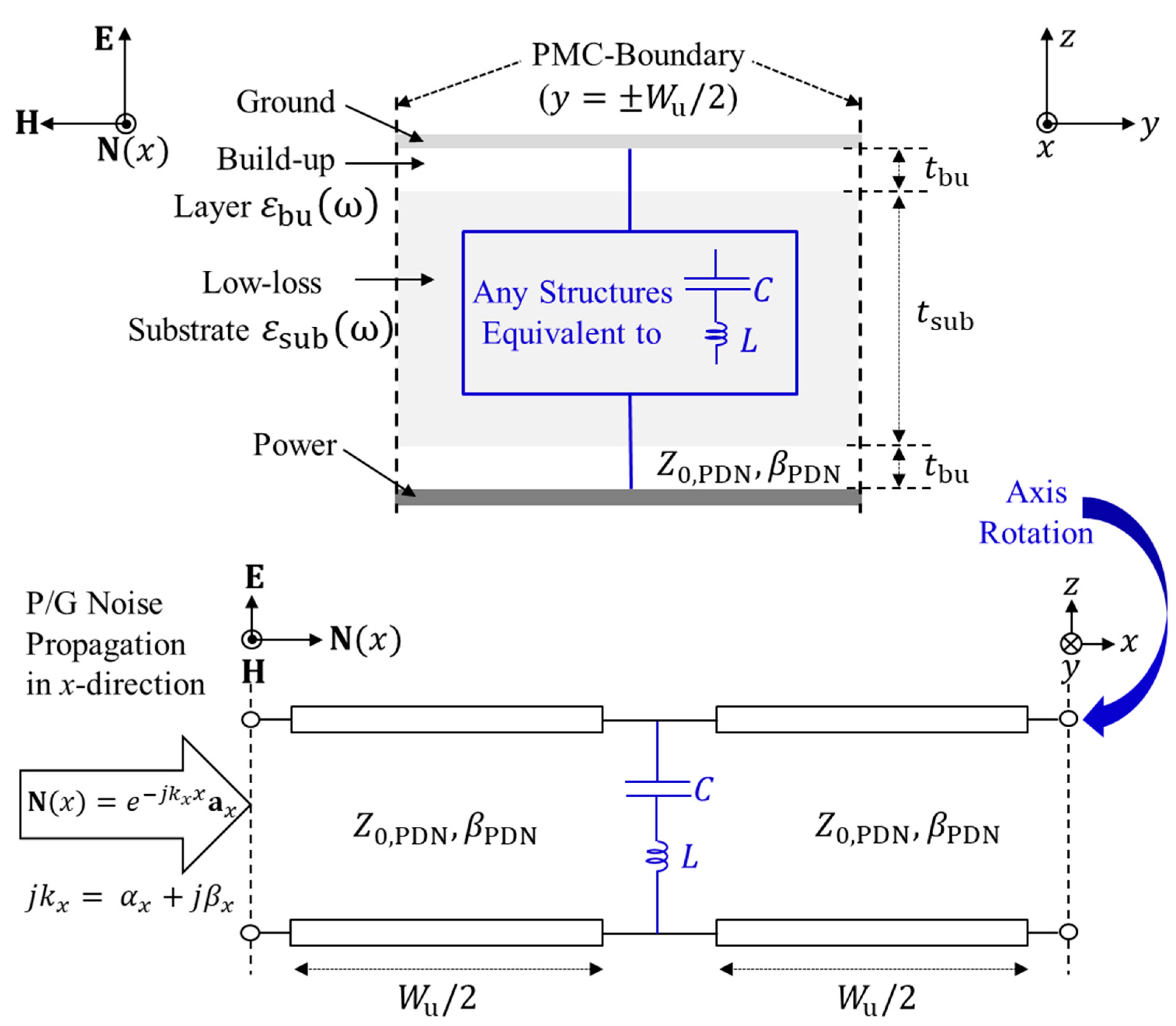
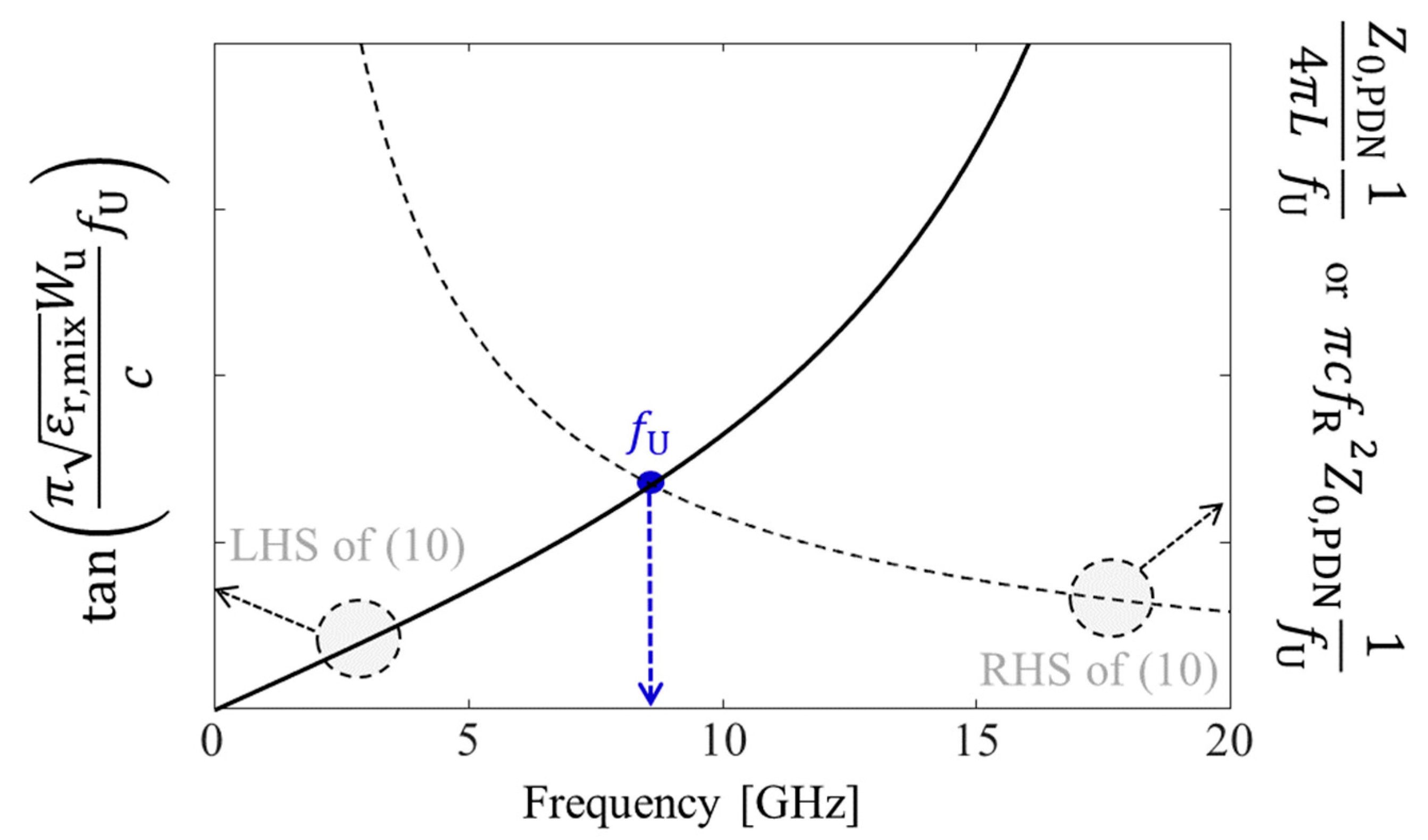
2. Proposed Dispersion Analysis: Mechanism of Noise Suppression Band Formation and Stopband Edge Estimation
3. Verification of the Proposed Dispersion Analysis and Noise Suppression Structures
3.1. Design and Fabricated Test Vehicles
3.2. Verification by Measurement and EM Simulation
4. Design and Analysis of Noise Suppression Structures with Various Low-Loss Materials
4.1. Noise Suppression Band Formulation with Various Materials
4.2. Impacts of Power/Ground Noise Decoupling Using the Proposed Structures
5. Conclusions
Funding
Conflicts of Interest
References
- Pak, J.; Ryu, C.; Kim, J. Electrical Characterization of Trough Silicon Via (TSV) depending on Structural and Material Parameters based on 3D Full Wave Simulation. In Proceedings of the 2007 IEEE International Conference on Electronic Material and Packaging, Daejeon, Korea, 19–22 November 2007; pp. 1–6. [Google Scholar]
- Tummala, R.; Sundaram, S.; Chatterjee, R.; Raj, P.M.; Kumbhat, N.; Sukumaran, V.; Sridharan, V.; Choudury, A.; Chen, Q.; Bandyopadhyay, T. Trend from ICs to 3D ICs to 3D systems. In Proceedings of the IEEE Custom Integrated Circuits Conference, San Jose, CA, USA, 13–16 September 2009; pp. 439–444. [Google Scholar]
- Swaminathan, M.; Han, K. Design and Modeling for 3D ICs and Interposers; World Scientific Publishing Co. Pte. Ltd.: Singapore, 2014; ISBN 978-981-4508-59-9. [Google Scholar]
- Technology Roadmap of DRAM for Three Major Manufacturers: Samsung, SK-Hynix and Micron. Available online: https://docplayer.net/29965569-Technology-roadmap-of-dram-for-three-major-manufacturers-samsung-sk-hynix-and-micron-may-2013.html (accessed on 30 May 2013).
- Lim, S. Design for High Performance, and Reliable 3D Integrated Circuits; Springer: Berlin/Heidelberg, Germany, 2013. [Google Scholar] [CrossRef]
- Standard JESD235A; High Bandwidth Memory (HBM) DRAM. JEDEC: Arlington, VA, USA, 2015.
- Cho, K.; Kim, Y.; Lee, H.; Kim, H.; Choi, S.; Song, J.; Kim, S.; Park, J.; Lee, S.; Kim, J. Signal Integrity Design and Analysis of Silicon Interposer for GPU-Memory Channels in High-Bandwidth Memory Interface. IEEE Trans. Compon. Packag. Manuf. Technol. 2018, 8, 1658–1671. [Google Scholar] [CrossRef]
- Kim, H.; Lee, H.; Cho, J.; Kim, Y.; Kim, J. Electrical Design of silicon, glass and organic interposer channels. In Proceedings of the 2014 Pan Pacific Microelectronics Symposium, Kauai, HI, USA, 3 February 2014. [Google Scholar]
- Sukumaran, V.; Bandyopadhyay, T.; Sundaram, V.; Tummala, R. Low-cost thin glass interposers as a superior alternative to silicon and organic interposers for packaging of 3-D ICs. IEEE Trans. Compon. Packag. Manuf. 2012, 2, 1426–1433. [Google Scholar] [CrossRef]
- Hu, D.C.; Hung, Y.; Chen, T.; Tain, R.; Lo, W. Embedded glass interposer for heterogeneous multi-chip integration. In Proceedings of the IEEE Electronic Components and Technology Conference (ECTC), San Diego, CA, USA, 26–29 May 2015; pp. 314–317. [Google Scholar]
- Lu, H.; Furuya, R.; Sawyer, B.M.; Nair, C.; Liu, F.; Sundaram, V.; Tummala, R.R. Design, modeling, fabrication and characterization of 2-5 μm redistribution layer traces by advanced semi-additive processes on low-cost panel based glass interposers. IEEE Trans. Compon. Packag. Manuf. 2016, 6, 959–967. [Google Scholar] [CrossRef]
- Park, G.; Cho, K.; Son, K.; Park, H.; Lho, D.; Kim, S.; Shin, T.; Kim, Y.; Kim, J.; Watanabe, A.; et al. Design and Measurement of a 28 GHz Glass Band Pass Filter based on Glass Interposers for 5G Applications. In Proceedings of the 2019 IEEE Electrical Design of Advanced Packaging and Systems Symposium, Kaohsiung, Taiwan, 16–18 December 2019. [Google Scholar]
- Laakso, M.J.; Bleiker, S.J.; Liljeholm, J.; Martensson, G.E.; Asiatici, M.; Fischer, A.C.; Stemme, G.; Ebefors, T.; Niklaus, F. Through-Glass Vias for Glass Interposers and MEMS Packaging Applications Fabricated Using Magnetic Assembly of Microscale Metal Wires. IEEE Access. 2018, 6, 44306–44317. [Google Scholar] [CrossRef]
- Tschoban, C.; Rossi, M.; Reyes, J.; Ndip, I.; Lang, K. Development of a Glass Technology Based 79 GHz MIMO Radar Front-End Module for Autonomous Driving. In Proceedings of the 2019 IEEE 21st Electronics Packaging Technology Conference, Singapore, 4–6 December 2019; pp. 376–381. [Google Scholar]
- Chang, Y.-H.; Chen, J.-C.; Chung, W.; Li, W.-Y.; Shih, P.-T.B.; Ng’Oma, A.; Yang, C.; Huang, M.-C.; Lin, H.-Y.; Wang, C.-H.; et al. A Novel Fabrication Process and Measurement Results of a 28 GHz Glass Antenna with Single TGV for 5G Communication Applications. In Proceedings of the 2019 14th International Microsystems, Packaging, Assembly and Circuits Technology Conference, Taipei, Taiwan, 23–25 October 2019; pp. 112–115. [Google Scholar]
- Hwangbo, S.; Yoon, Y.; Shorey, A. Glass Interposer Integrated Dual-band Millimeter Wave TGV Antenna for Inter-/Intra Chip and Board Communications. In Proceedings of the 2016 IEEE International Symposium on Antennas and Propagation, Fajardo, Puerto Rico, 26 June–1 July2016; pp. 1639–1640. [Google Scholar]
- Kim., Y.; Kim, Y.; Cho, K.; Park, G.; Kim, S.; Kang, K.; So, K.; Jeon, J.; Kim, C.; Paik, W. Power and Signal Integrity Analysis of Fan-out Wafer Level Package for Mobile Application Processor. In Proceedings of the DesignCon 2017, Santa Clara, CA, USA, 30 January 2017. [Google Scholar]
- FaradFlex for PCBs. Available online: https:/www.faradflex.com/pcbs/ (accessed on 1 April 2022).
- Kitazawa, T.; Hayashi, Y.; Fukawa, Y.; Kim, Y. Analysis of the PDN Induced Crosstalk Impacts on the High-speed Signaling in Ultra-thin and High Permittivity Substrates. In Proceedings of the EMC Europe 2022, Gothenburg, Sweden, 5–8 September 2022. [Google Scholar]
- Kim, Y.; Kim, K.; Cho, J.; Kim, J.; Sundaram, V.; Tummala, R. Analysis of Power Distribution Network in Glass, Silicon Interposer and PCB. In Proceedings of the 2014 IEEE International Symposium on Electromagnetic Compatibility, Raleigh, NC, USA, 5 August 2014. [Google Scholar]
- Hashimoto, M.; Nair, R. Power Integrity for Nanoscale Integrated Systems; McGraw-Hill Education: New York, NY, USA, 2014; ISBN 978-0-07-178776-5. [Google Scholar]
- Kim, Y.; Wada, S.; Fujimoto, D.; Hayashi, Y. Analysis of Electromagnetic Information Leakage from Overdesigned Power Delivery Network of Cryptographic Devices. In Proceedings of the 2021 Asia Pacific International Symposium on Electromagnetic Compatibility, Hybrid (Bali & On-line), 28 September 2021. [Google Scholar]
- Wada, S.; Hayashi, Y.; Fujimoto, D.; Homma, N.; Kim, Y. Measurement and Analysis of Electromagnetic Information Leakage from Printed Circuit Board Power Delivery Network of Cryptographic Devices. IEEE Trans. Electromagn. Compat. 2021, 63, 1322–1332. [Google Scholar] [CrossRef]
- Rogers, S.D. Electromagnetic-bandgap Layers for Broad-band Suppression of TEM modes in Power Planes. IEEE Trans. Microw. Theory Tech. 2005, 53, 2495–2505. [Google Scholar] [CrossRef]
- Toyota, Y.; Engin, A.; Kim, T.; Swaminathan, M. Stopband Analysis Using Dispersion Diagram for Two-Dimensional Electromagnetic Bandgap Structures in Printed Circuit Boards. IEEE Microw. Wirel. Compon. Lett. 2006, 16, 645–647. [Google Scholar] [CrossRef]
- Kim, L.; Schutt-Aine, J. Analysis and Modeling of Hybrid Planar-Type Electromagnetic-Bandgap Structures and Feasibility Study on Power Distribution Network Applications. IEEE Trans. Microw. Theory Tech. 2008, 56, 178–186. [Google Scholar] [CrossRef]
- Hwang, C.; Shim, Y.; Koo, K.; Kim, M.; Pak, J.; Kim, J. An On-Chip Electromagnetic Bandgap Structure using an On-Chip Inductor and a MOS Capacitor. Microw. Wirel. Compon. Lett. 2011, 21, 439–441. [Google Scholar] [CrossRef]
- Wei, P.; Tsai, M.; Hsu, S.; Shen, C.; Wu, T. An Electromagnetic Bandgap Structure Integrated with RF LNA Using Integrated Fan-Out Wafer-Level Package for Gigahertz Noise Suppression. IEEE Trans. Microw. Theory Tech. 2018, 66, 5482–5490. [Google Scholar] [CrossRef]
- Das, R.; Yoo, H. Application of a Compact Electromagnetic Bandgap Array in a Phone Case for Suppression of Mobile Phone Radiation Exposure. IEEE Trans. Microw. Theory Tech. 2018, 66, 2363–2372. [Google Scholar] [CrossRef]
- Zhu, H.; Wang, J.; Sun, Y.; Wu, X.; Mao, J. A Novel Automatically Designed EBG Structure by Improved GA for Ultrawideband SSN Mitigation of System in Package. IEEE Trans. Compon. Packag. Manuf. Technol. 2020, 10, 123–133. [Google Scholar] [CrossRef]
- Kim, M.; Koo, K.; Hwang, C.; Shim, Y.; Kim, J.; Kim, J. A Compact and Wideband Electromagnetic Bandgap Structure Using a Defected Ground Structure for Power/Ground Noise Suppression in Multilayer Packages and PCBs. IEEE Trans. Electromagn. Compat. 2012, 54, 689–695. [Google Scholar]
- Kim, K.; Hwang, C.; Koo, K.; Cho, J.; Kim, H.; Kim, J.; Lee, J.; Lee, H.; Park, K.; Pak, J. Modeling and Analysis of a Power Distribution Network in 3-D Memory IC Including P/G TSVs, On-chip Decoupling Capacitors, and Silicon Substrate Effects. IEEE Trans. Compon. Packag. Manuf. Technol. 2012, 2, 2057–2070. [Google Scholar] [CrossRef]
- Kim, K.; Yook, J.; Kim, J.; Kim, H.; Lee, J.; Park, K.; Kim, J. Interposer Power Distribution Network Modeling Using a Segmentation Method for 3-D ICs with TSVs. IEEE Trans. Compon. Packag. Manuf. Technol. 2013, 3, 1891–1906. [Google Scholar] [CrossRef]
- Tuncer, E.; Serdyuk, Y.V.; Gubanski, S.M. Dielectric mixtures: Electrical properties and modeling. IEEE Trans. Dielectric. Electr. Insul. 2002, 9, 809–828. [Google Scholar] [CrossRef]
- McCann, S.R.; Sato, Y.; Sundaram, V.; Tummala, R.; Sitaraman, K. Prevention of Cracking from RDL Stress and Dicing Defects in Glass Substrates. IEEE Trans. Device Mater. Reliab. 2016, 16, 43–49. [Google Scholar] [CrossRef]
- Kim, Y.; Cho, J.; Kim, J.J.; Kim, K.; Cho, K.; Kim, S.; Sitaraman, S.; Sundaram, V.; Raj, P.M.; Tummala, R.; et al. Measurement and Analysis of Glass Interposer Power Distribution Network Resonance Effects on a High-Speed Through Glass Via Channel. IEEE Trans. Electromagn. Compat. 2016, 58, 1747–1759. [Google Scholar] [CrossRef]
- Kim, Y.; Park, G.; Cho, K.; Raj, P.M.; Tummala, R.R.; Kim, J. Wideband Power/Ground Noise Suppression in Low-Loss Glass Interposers Using a Double-Sided Electromagnetic Bandgap Structure. IEEE Trans. Microw. Theory Tech. 2020, 68, 5055–5064. [Google Scholar] [CrossRef]
- Pozar, D. Microwave Engineering, 3rd ed.; John Wiley and Sons: Hoboken, NJ, USA, 2005. [Google Scholar]
- Clavijo, S. Design Methodology for Sievenpiper High-impedance Surfaces. M.S. Thesis, Department of Electrical Engineering, Arizona State University, Tempe, AZ, USA, 2002. [Google Scholar]
- 2.5D Interposer for High Bandwidth: Design, Fabrication and Characterization. Available online: http://www.prc.gatech.edu/sites/default/files/documents/iab_spring2016/Presentations/Wednesday%20Presentations/09%20IAB_May_2016-DDTV_2.5DGIP%20Brett%20Sawyer.pdf (accessed on 1 December 2016).


| L | C | |||
|---|---|---|---|---|
| 4.25 | 9.14 | 3.2 mm | 125.49 pH | 22.831 pF |
| Symbol | Type A | Type B | |
|---|---|---|---|
| Physical Dimensions | tsub | 100 | |
| tbu1 | 15 | 17.5 | |
| tbu2 | 15 | 35 | |
| tm | 3~5 | 4~10 | |
| dTGV_T | 60 | 100 | |
| dTGV_B | 40 | 60 | |
| d_T | 35 | 45 | |
| d_B | 30 | 45 | |
| Wu | 3.2 mm | ||
| Wpa | 2.2 mm | ||
| 300 | NA | ||
| 5.3 @ 2.4 GHz | 5.3 @ 2.4 GHz | ||
| 3.2 @ 5.8 GHz | 3 @ 10 GHz | ||
| Material Properties | tansub | 0.004 @ 2.4 GHz | 0.004 @ 2.4 GHz |
| tanbu | 0.0042 @ 5.8 GHz | 0.005 @ 10 GHz | |
| m | 5.8 | ||
| Structures | Edges | Measurement | Simulation (Error) | Estimation (Error) |
|---|---|---|---|---|
| Type A | 2.51 GHz | 2.49 GHz (1.00%) | 2.51 GHz (0.04%) | |
| 8.91 GHz | 8.75 GHz (1.83%) | 8.59 GHz (3.61%) | ||
| Type B | 5.82 GHz | 5.50 GHz (5.49%) | 5.87 GHz (0.86%) | |
| 9.66 GHz | 9.75 GHz (0.93%) | 10.4 GHz (7.66%) |
| Band Expansion | Design Parameters | Impacts | Note |
|---|---|---|---|
| High-K materials in BU | C | ||
| Thin BU materials | C | ||
| Larger pactes (Wpa) | C | Limited | |
| Increase package/interposer and PDN thickness (tPDN) | Not desired | ||
| Add defects in P/G planes | L | Limited | |
| Through via diameter | L | Limited & 1/ | |
| Through via diameter | L | 1/L | |
| Via arrays or parallel vias | L | 1/L | |
| Z0,PDN(t PDN) | RSH of (10) | Not desired | |
| Structures | Eye-Opening Voltage | Jitter (% of UI) | P/G Noise at 0 or 1 |
|---|---|---|---|
| Type A | 784 mV 838 mV | 36.5 ps (7.1)22.2 ps (4.4) | 60 mV 19 mV |
| Type B (Figure 13) | 1.08 V 1.15 V | 18 ps (3.6)7 ps (1.4) | 62 mV mV |
| FaradFlex based (Figure 10) | 1.05 V 1.11 V | 21 ps (4.2)13 ps (2.6) | 70 mV mV |
Publisher’s Note: MDPI stays neutral with regard to jurisdictional claims in published maps and institutional affiliations. |
© 2022 by the author. Licensee MDPI, Basel, Switzerland. This article is an open access article distributed under the terms and conditions of the Creative Commons Attribution (CC BY) license (https://creativecommons.org/licenses/by/4.0/).
Share and Cite
Kim, Y. Design of Power/Ground Noise Suppression Structures Based on a Dispersion Analysis for Packages and Interposers with Low-Loss Substrates. Micromachines 2022, 13, 1433. https://doi.org/10.3390/mi13091433
Kim Y. Design of Power/Ground Noise Suppression Structures Based on a Dispersion Analysis for Packages and Interposers with Low-Loss Substrates. Micromachines. 2022; 13(9):1433. https://doi.org/10.3390/mi13091433
Chicago/Turabian StyleKim, Youngwoo. 2022. "Design of Power/Ground Noise Suppression Structures Based on a Dispersion Analysis for Packages and Interposers with Low-Loss Substrates" Micromachines 13, no. 9: 1433. https://doi.org/10.3390/mi13091433