Article

Investigation on Capacitance Collapse Induced by Secondary Capture of Acceptor Traps in AlGaN/GaN Lateral Schottky Barrier Diode

1
High-Frequency High-Voltage Device and Integrated Circuits Center, Institute of Microelectronics of Chinese Academy of Sciences, Beijing 100029, China
2
School of Electronic Electrical and Communication Engineering, University of Chinese Academy of Sciences, Beijing 100049, China
3
The Institute of Future Lighting, Academy for Engineering and Technology, Fudan University (FAET), Shanghai 200433, China
*
Authors to whom correspondence should be addressed.
Micromachines 2022, 13(5), 748; https://doi.org/10.3390/mi13050748
Submission received: 31 March 2022 / Revised: 5 May 2022 / Accepted: 6 May 2022 / Published: 9 May 2022
(This article belongs to the Special Issue GaN-Based Semiconductor Devices)

Abstract

:
In this study, a dedicated dynamic measurement system was used to investigate the transient capacitance and recovery process of AlGaN/GaN lateral Schottky barrier diodes (SBDs). With the consideration of acceptor traps in the C-doped buffer, the C-V characteristics and transient capacitance were measured and analyzed, and the results were simulated and explained by Silvaco TCAD (technology computer aided design). The ionization of acceptor traps and the change of electric potential were monitored in transient simulation to investigate the origin of the capacitance collapse in the SBD. The results suggest the significant impact of traps in the GaN buffer layer on the capacitance collapse of the device, and the secondary capture effect on the variation of acceptor ionization. Based on the study of transient capacitance of SBD, this work could be extended to the Miller capacitance in high electron mobility transistor (HEMT) devices. Moreover, the report on the stability of capacitance is essential for GaN devices, and could be further extended to other aspects of device research.

1. Introduction

Gallium nitride devices are widely used in radio frequency (RF) and power switching circuits. However, parasitic capacitance in gallium nitride devices is problematic in its further improvements [1,2]. Here, we focus on the capacitance of thin-barrier AlGaN/GaN heterojunction Schottky barrier diodes (SBDs). It can be equivalently viewed as a capacitance between gate and drain (Cgd) in high electron mobility transistor (HEMT) devices if adding an extra ohmic cathode. Cgd refers to the Miller capacitance of HEMT devices [3]. For power devices and RF devices, Cgd is the most important parasitic capacitance parameter [4]. The instability of Cgd will significantly affect the performance and stability of the equipment, and the change of capacitance of RF devices is directly related to the impedance matching of the circuit. If the capacitance value considerably fluctuates with RF electrical stress, it will result in change in RF circuit bandwidth, insertion loss and other problems [5,6,7]. The stability of capacitance is very important for gallium nitride devices. The existing body of research has recognized the degradation phenomenon after stressing during the RF operation, but no clear relationship has been established between device degradation, trapping effect and capacitance, and the degradation mechanism still remains problematic [8,9].
In this work, we mainly focus on the capacitance of thin-barrier AlGaN/GaN heterojunction Schottky barrier diodes. The ultra-thin barrier AlGaN and the ultra-thin SiN dielectric could substantially improve the capacitance caused by the field plate ([10], pp. 202–206). The change effect of capacitance is amplified by increasing the capacitance ratio brought by field plate, and the change of capacitance after stress could be well observed.
In our previous work [11,12,13], a model of an ultra-thin barrier gallium nitride SBD device with improved accuracy is carried out. In particular, the current collapse is studied in detail. In this paper, we firstly propose the concept of “capacitance collapse”. Different from the current collapse test, capacitance collapse monitors the capacitance value before and after the electrical stress instead of current monitoring. Therefore, capacitance collapse tests cannot be performed with conventional equipment. An AccoTEST STS8200 tester has been modified to quickly switch between capacitance monitoring and reverse high voltage stress.
The curve of capacitance collapse is well fitted with the correction from the simulation model. By studying the ionization of the acceptor traps and potential changes in the corrected model, the origin of capacitance collapse is discussed. The ionization of acceptor traps leads to the change of potential in GaN, leading to a changing depletion layer width in GaN and thus the change of capacitance. The secondary capture effect results in different levels of acceptor ionization. This study provides a new idea for the research of capacitance of GaN devices, and it can be further extended to other aspects of device research.

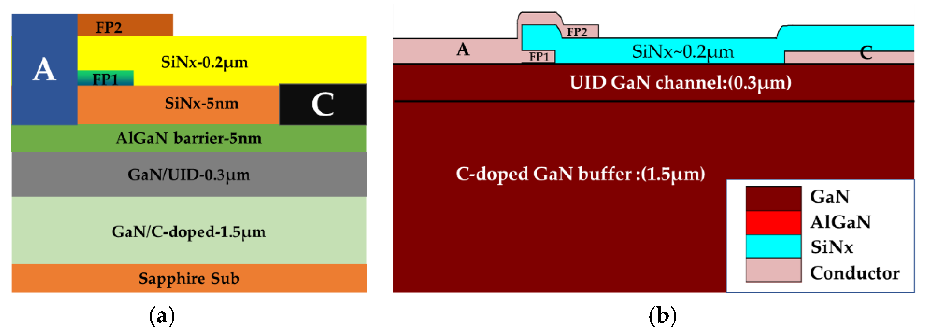
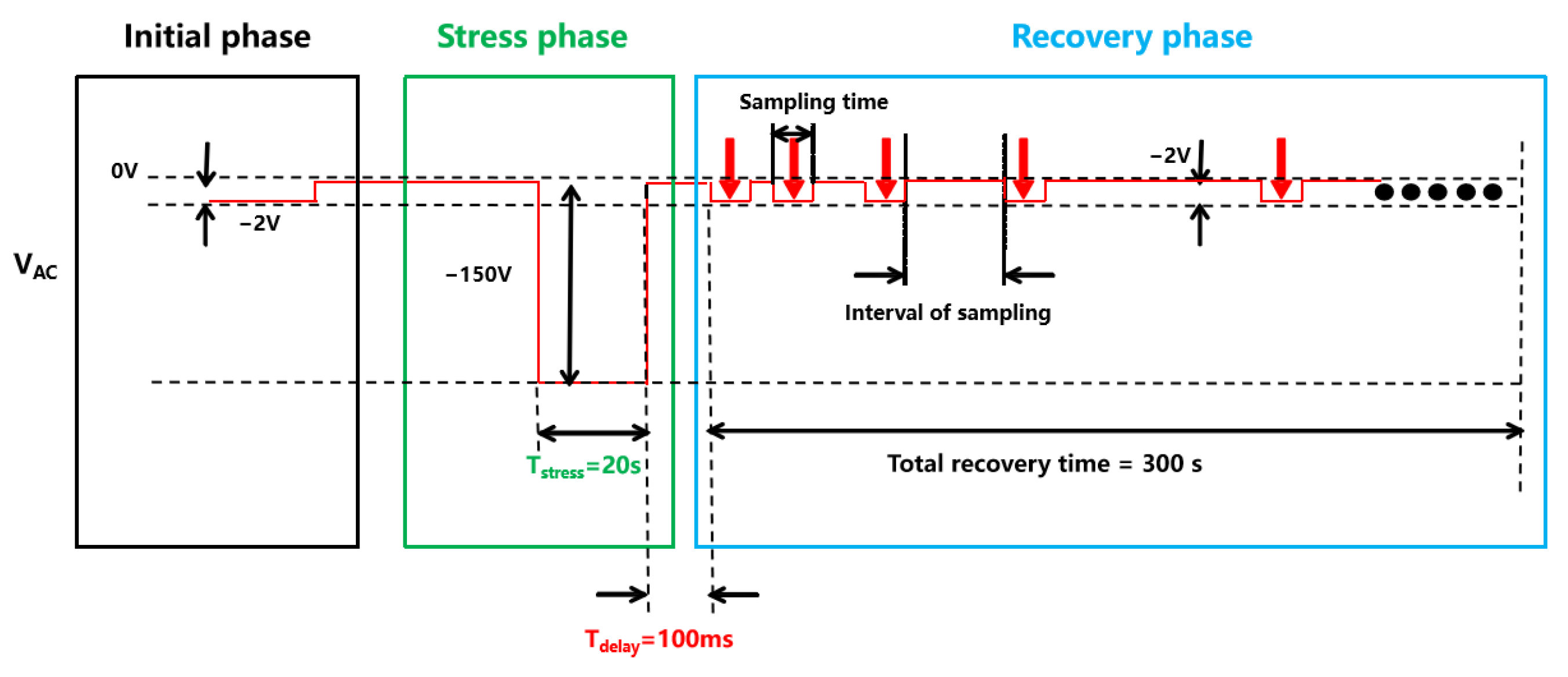
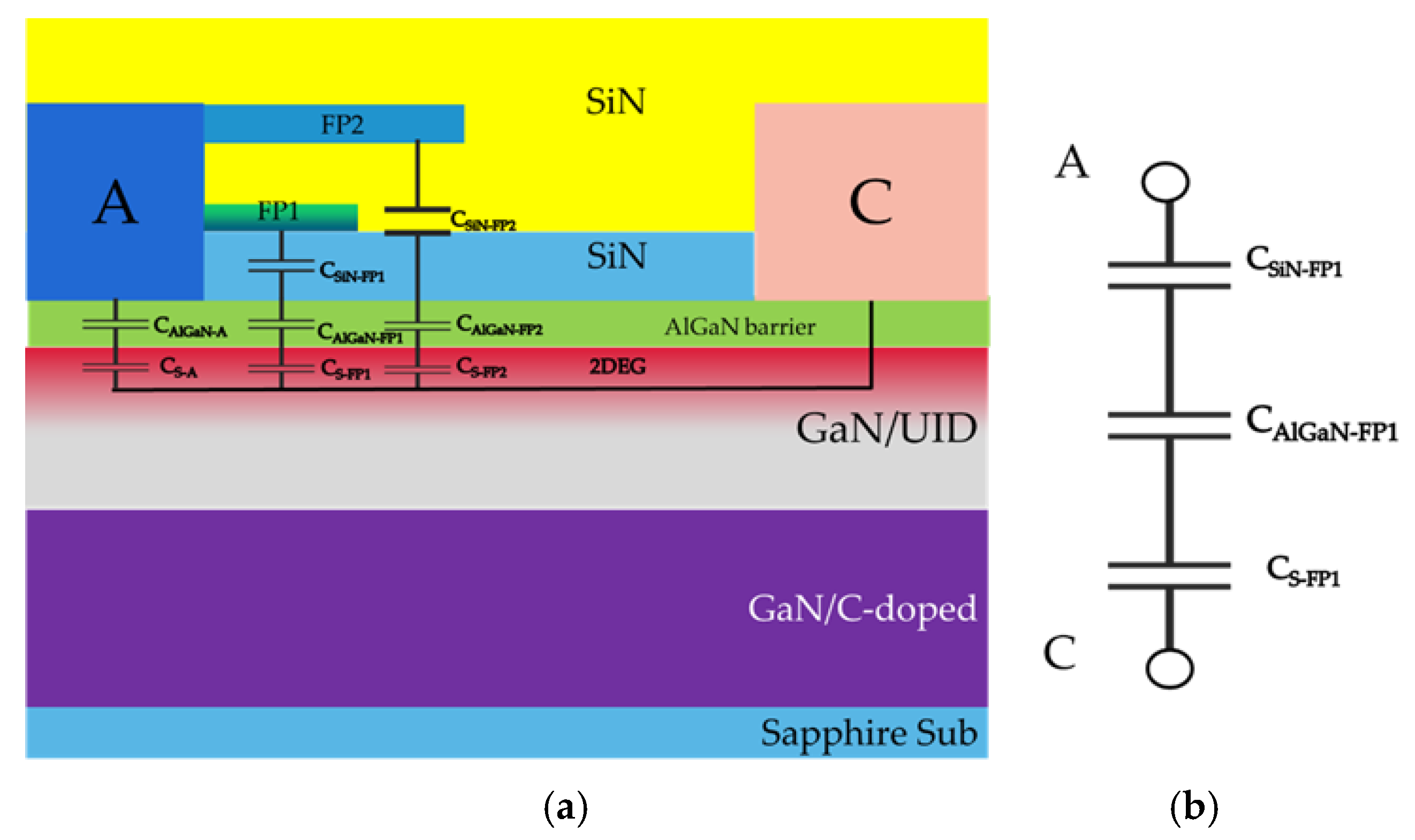
2. Device Characterization and Simulation

The schematic of the SBD is shown in Figure 1. Metal organic chemical vapor deposition (MOCVD) was used to deposit the AlGaN/GaN heterostructure on 4-inch sapphire substrate. The smooth and crack-free epitaxial layer consists of a carbon-doped GaN buffer layer, a GaN channel, an AlN interface enhancement layer and a Al0.25Ga0.75N barrier with thicknesses of 1.5 μm/300 nm/1 nm and 5 nm. Two layers of field plates, namely FP1 and FP2, were progressively deposited with a 5 nm pre-grown LPCVD SiNx and a 200 nm interlayer SiNx.
The dynamic measurement sequence is summarized in Figure 2. At the initial phase, the initial capacitance (CCA) was measured as fabricated with an STS8200 at VAC = −1.8 V and f = 1 MHz. During the second phase, the stress phase, a stress voltage (VAC) of −150 V was applied with a total stress time (tstress) of 20 s. After stressing, the recover capacitance CCA (at VAC = −1.8 V and f = 1 MHz) was measured immediately with a delay time (tdelay) of 100 ms in the recovery phase. The interval between each sampling period was gradually increased with a total recovery time of 300 s. The dynamic characteristic simulation and the electrical measurement only differ in the constant VAC of −1.8 V and frequency of 1 MHz in the recovery phase.
Previously, we have discussed the main simulation key parameters in detail [13]. In this study, we adjusted the thickness of SiN from 10 nm to 5 nm in order to obtain more observable capacitance changes. Compared with our previous work, we improved and optimized the simulation model to minimize its discrepancy with our device structure, especially the morphology of the field plate, in order to guarantee the accuracy of the capacitance simulation. Some simulation key parameters have been fine-tuned: the energy level of acceptor traps (ETA) in C-doped buffer is adjusted to EV +0.95 eV and the donor trap energy level (ETD) is adjusted to EC −1.05 eV. The energy level of GaN is measured to be EC −1.10 eV in existing body of research [14], and the energy level of carbon doping of EV +0.9 eV has been extensively confirmed in previous studies [15,16,17,18,19,20,21,22]. The electrical measurements fit the simulation results well. Some simulated key parameters are summarized in Table 1.
Through the capture and emission of free carriers, the charge trapping effects can affect the electrical potential inside the device. For instance, as shown in Figure 3b, the deep-level acceptor traps in the GaN buffer layer (mainly in the C-doped region) would release holes under a high electric field, yielding negative space charges in the buffer layer [23,24]. These negative space charges would result in the reduction of the potential of C-doped GaN buffer layer. When entering the recovery phase, these negatively charged acceptor traps accumulating in GaN buffer start to capture holes from the valence band, recovering into an electrically neutral state, as shown in Figure 3c.

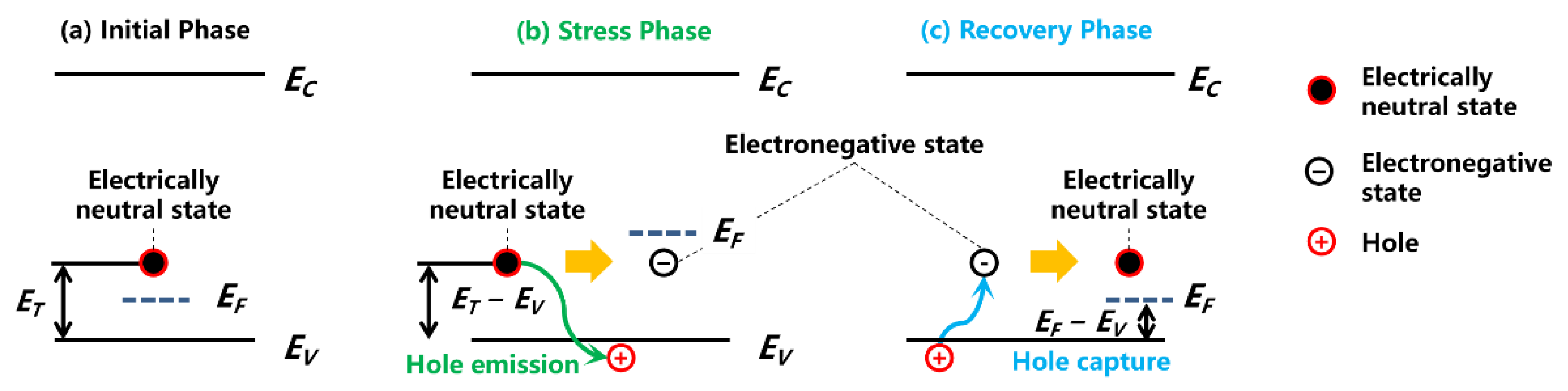
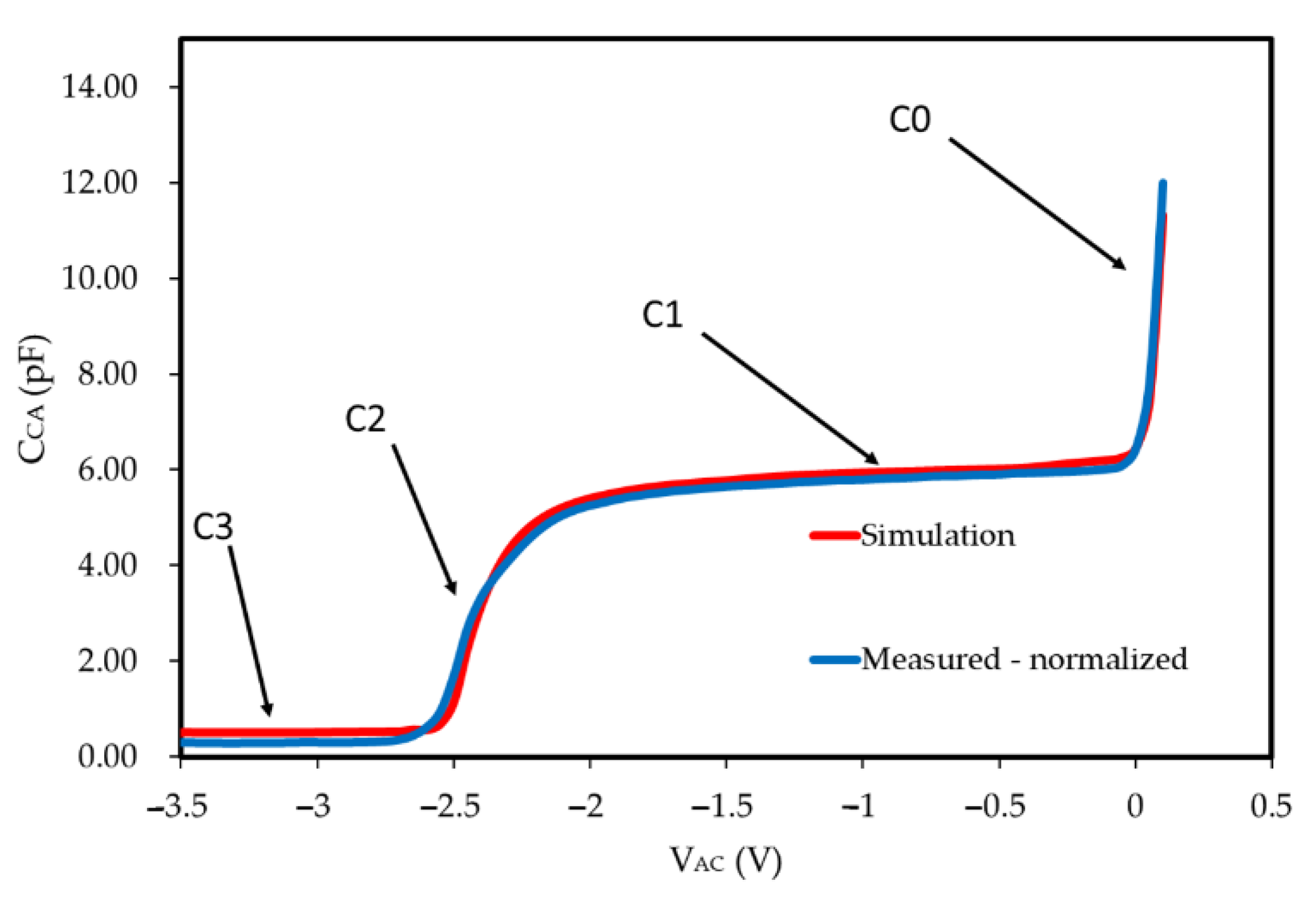
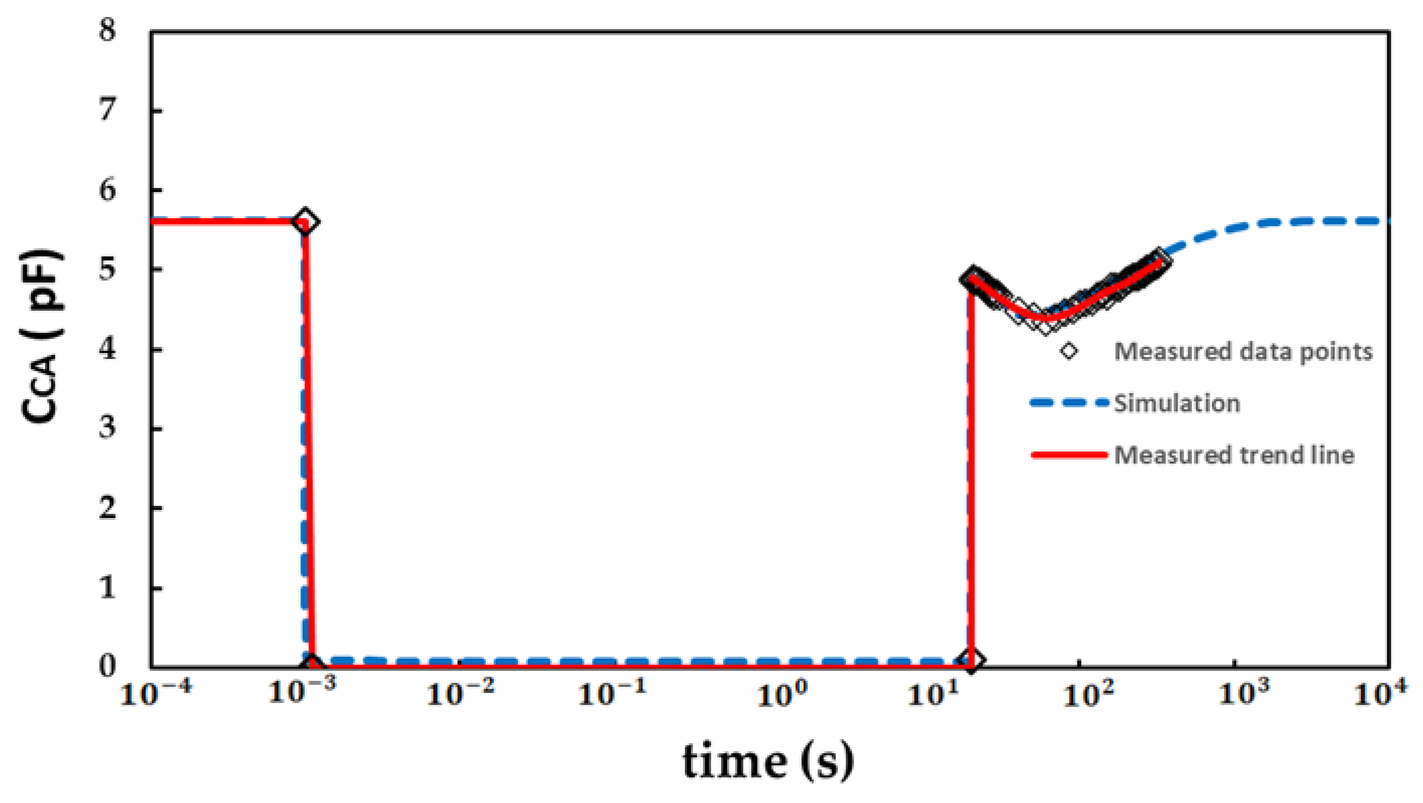
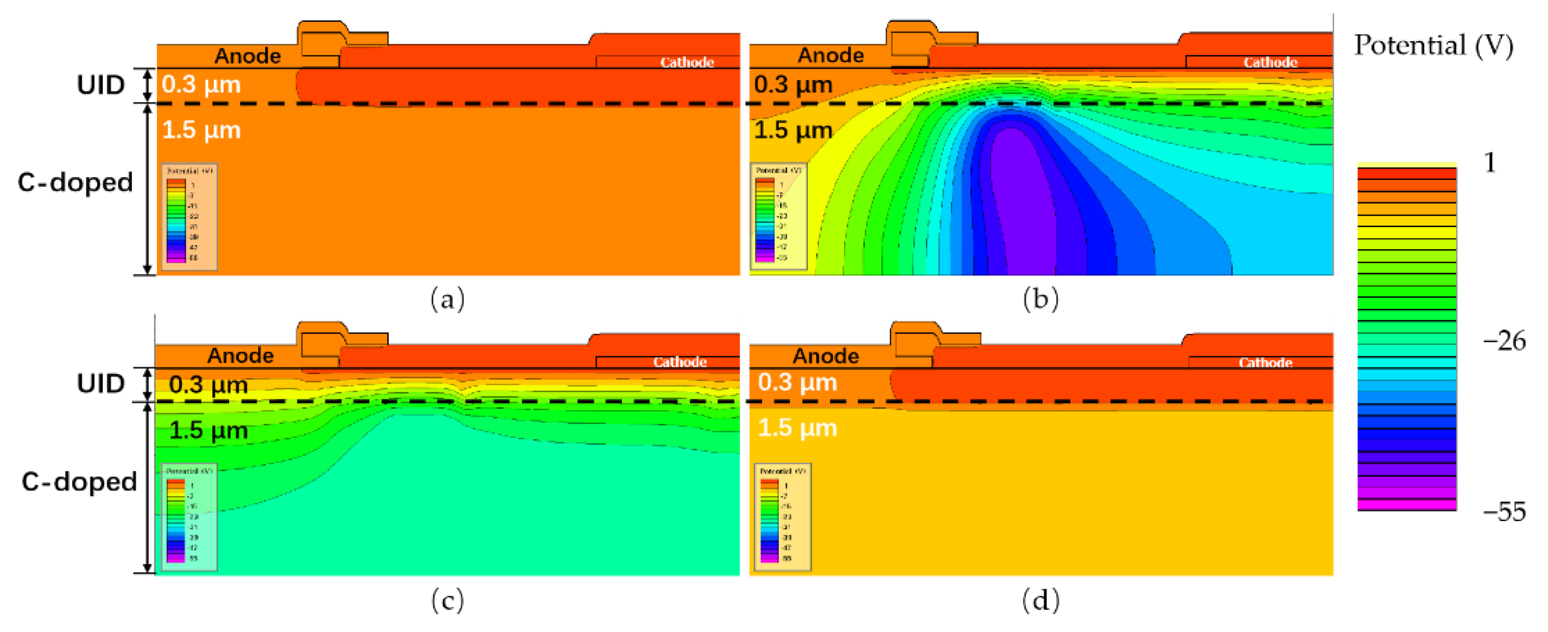
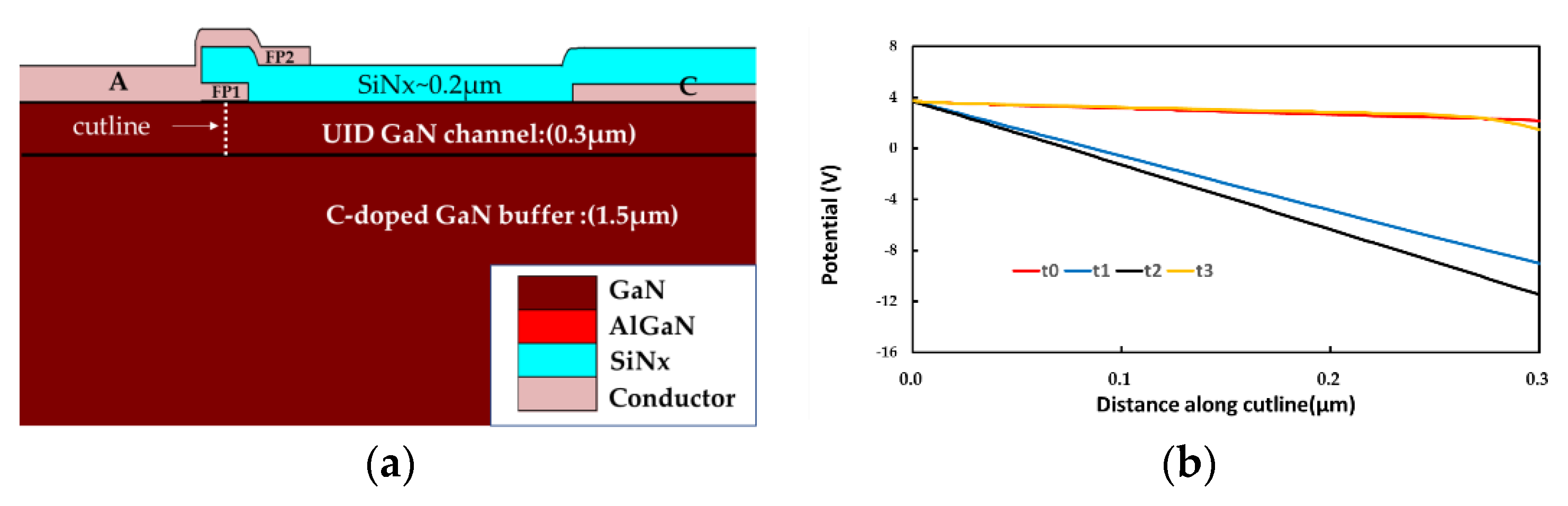
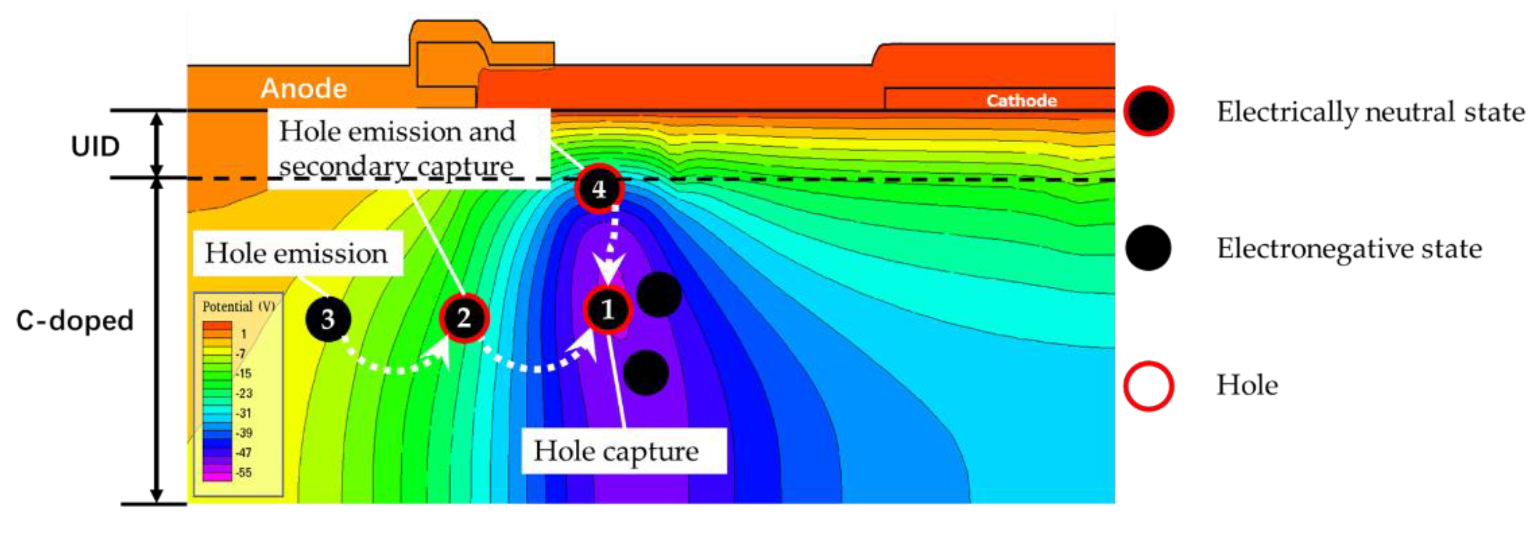
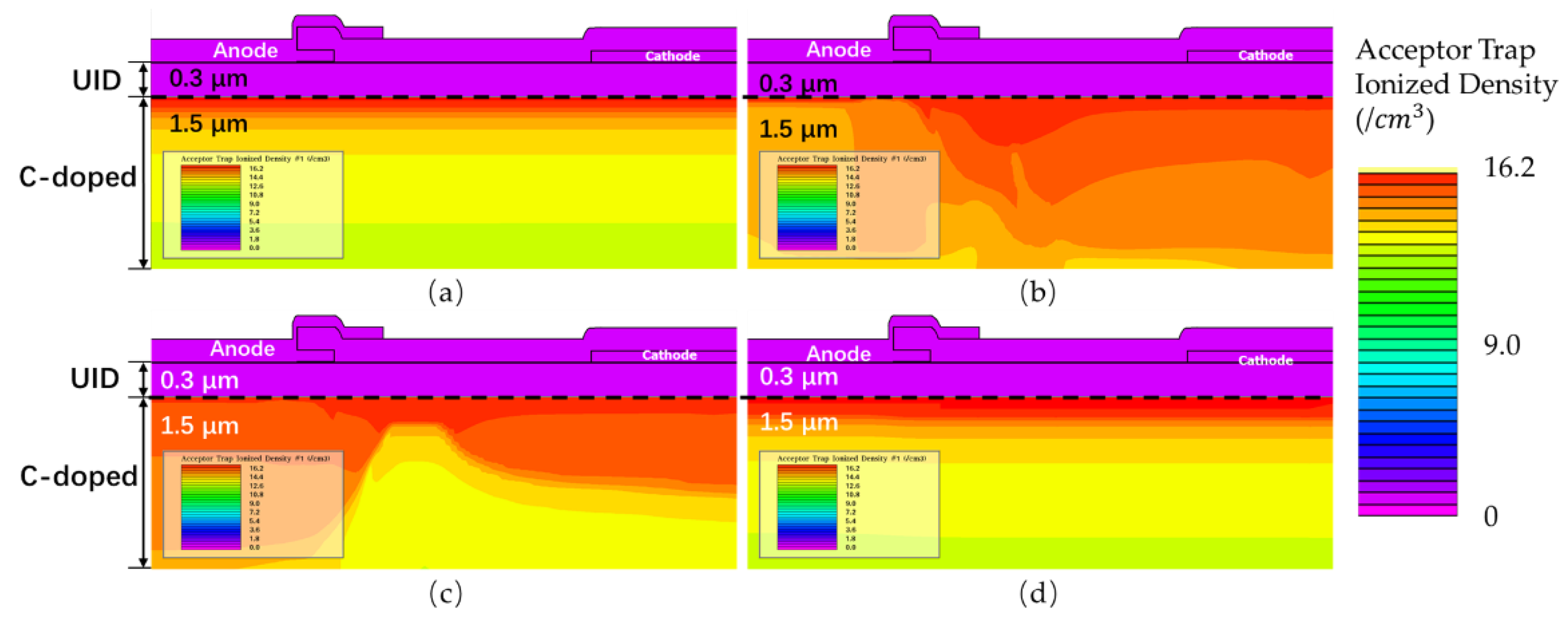
3. Results and Discussion

The C-V curve measurement was carried out on GaN SBDs with LAC = 6 μm. As could be observed from Figure 4, the measured and normalized C-V curve (in blue) relatively matches the simulated C-V curve (in red). The actual test capacitance is larger than the simulated capacitance because of the existence of auxiliary regions contributing to parasitic capacitance in the actual device structure. We normalized the actual capacitance according to the capacitance result at VAC = 0 V and the capacitance of the subsequent dynamic test. C0 is the depletion capacitance of 2DEG, C1 is the capacitance of FP, C2 is the depletion process of the 2DEG under FP, C3 is the drift region capacitance. As VAC becomes negative, the 2DEG below the anode is depleted. VAC continued to become negative and the capacitance of FP was depleted. As shown in Figure 4, the capacitance changes of the simulation and actual test maintain the same trend. There is a certain deviation between the simulation and the actual test, which is mainly caused by the differences in the doping concentration, dielectric thickness and polarization coefficient between the actual and simulated devices.
Figure 5 presents the parasitic capacitance model of the device and its equivalent circuit in reverse bias state (VAC = −1.8 V). The capacitance related to SiN and AlGaN is considered as a dielectric capacitance and is related to the dielectric constant, area and thickness of the dielectric. As could be observed from Figure 4, the 2DEG under anode metal has been depleted in the state of reverse bias. Therefore, the capacitance associated with the anode region can be ignored. Since the medium under FP2 is thicker, the capacitance of the field plate can only be equivalent to that of FP1. The change of device capacitance in reverse bias state (VAC = −1.8 V) is mainly influenced by the variation of the depletion layer in UID-GaN. CCA decreases with the increase of VCA, mainly because the high reverse bias would extend the depletion region, leading to the change of capacitance.
The capacitance of semiconductor devices in the depleted state could be estimated with the following relationship ([10], pp. 197–240):
C s = ε s ε 0 2 L D exp ( q V s 2 k T )
where C s is the semiconductor space charge layer capacitance, Vs is the surface potential across the space charge layer of GaN, ε s is the permittivity of the semiconductor, ε 0 is the permittivity of the vacuum, L D is the Debye length, k is the Boltzmann constant, T is the absolute temperature, q is the unit electronic charge.
The transient measurement was carried out on GaN SBDs with LAC = 6 μm. At the first phase (10−4 s to 10−3 s), the initial CCA (measured with VAC = −1.8 V, f = 1 MHz) was measured. At the stress phase (10−3 s to 20 s), the stress voltage VAC was set to be −150 V. At the recovery phase, the CCA was taken immediately after stressing with a delay time of 100 ms. Measured and simulated results with the model mentioned in the Section 2 are summarized in Figure 6 with solid and dotted lines, respectively. In the simulation, in order to improve the convergence of simulation model, we set the anode to zero potential and applied positive bias to the cathode to achieve the effect of reverse bias. In the simulation, the CCA gradually decreased at the first 20 s and gradually increased after 20 s and returned to the initial state. The measured result is in concordance with the simulation model.
Figure 7 shows the potential distribution diagram at different timings. In Figure 7b, the potential in the buffer layer reduces significantly after the reverse stress. In Figure 7c,d, the potential extremum is gradually lowered and recovered after a sufficient time delay.
Figure 8a presents the location of the cutline, which is in the UID region below the center of FP1. Figure 8b shows the changing trend of potential, and the potential difference reaching the maximum value at 20 s (t2). According to Equation (1), we could safely conclude that CCA reaches the minimum value at 20 s (t2).
Figure 9 shows the potential distribution measured at 1 s after the electrical stress was removed. The presence of electronegative states at position 1 results in its lower potential. The denser potential lines showing the higher electric field in the vicinity would promote the acceptor traps in the vicinity to still have a higher ionization rate, even after the removal of stress. The acceptor traps at positions 2 and 4 ionize and release the holes captured by the electronegative state at position 1 under the action of potential difference. The electronegative state at position 1 captures the hole and restores the electrically neutral state, thus increasing the negative potential value. The ionized acceptor traps at position 2 will release holes and turn into an electronegative state, but the ionized acceptor traps at position 2 will capture the hole released by the acceptor traps at position 3 and restore the electrically neutral state. The continuously ionized and captured acceptor defect at position 2 could be viewed as “secondary capture”. The acceptor traps near position 3 are continuously ionized, while the holes released are captured by the electronegative state at position 2. However, no hole can restore the electric neutrality at position 3. Therefore, a large number of acceptor traps at position 3 would become electronegative, thus lowering the electric potential at position 3. Through this process, the potential at position 1 will continue to levitate, while the potential at position 3 will continue to fall.
As time goes by, the potential difference between position 3 and position 1 reduces to a level with no allowance for the “secondary capture” of the acceptor traps at position 2. The potential at position 1 no longer decreases. It occurs at the time node of about 20 s after the removal of electrical stress in simulation. Afterwards, the overall potential in the buffer layer increases and thus the potential difference in the UID-GaN gradually decreases and eventually returns to its initial state. According to our previous analysis, the change of potential difference in UID-GaN would result in capacitance variation. The minimum value of capacitance appears at about 20 s after the removal of the electrical stress, which is consistent with the trend of potential change.
Figure 10 shows the acceptor trap ionized distribution diagram at different times. In Figure 10b, the ionization concentration of acceptor traps reaches its maximum near the position of lowest potential. In Figure 10c, the ionization concentration is higher at position 3 in Figure 9. In Figure 10d the acceptor trap ionization is gradually lowered and recovered after a sufficient time delay. These observations are consistent with our analysis of the process of “secondary capture”.

4. Conclusions

Capacitance collapse characterization on a lateral AlGaN/GaN SBD was successfully carried out with a modified AccoTEST STS8200 tester. C-V characteristics and dynamic capacitance well matched the simulations from Silvaco TCAD. Based on our well-verified model, the variation of electric potential and the ionization of acceptor traps in the device were studied and analyzed in detail. The relationship between the electric potential and acceptor traps was simulated and discussed by varying the capture and emission of the acceptor traps. The “secondary capture” effect resulted in different variation levels of the acceptor ionization, leading to various potential changes and subsequently the capacitance change of the device. This study of SBD devices can be extended to the study of Miller capacitance of HEMT devices.

Author Contributions

H.Z., writing—original draft; X.K., review and editing; Y.Z., H.W. and K.W., data curation; Z.J., X.L. and T.Y., project administration. All authors have read and agreed to the published version of the manuscript.

Funding

This work was supported in part by the Key-Area Research and Development Program of the Guang Dong Province (No. 2019B010128001); and in part by the Youth Innovation Promotion Association of CAS.

Institutional Review Board Statement

Not applicable.

Informed Consent Statement

Not applicable.

Data Availability Statement

Not applicable.

Conflicts of Interest

The authors declare no conflict of interest.

References

  1. Yong, W.; Yu, N.; Deng, D.; Ming, L.; Lau, K. Improved AlGaN/GaN HEMTs Grown on Si Substrates by MOCVD. In Proceedings of the 2010 Academic Symposium on Optoelectronics and Microelectronics Technology and 10th Chinese-Russian Symposium on Laser Physics and Laser Technology Optoelectronics Technology (ASOT), Harbin, China, 28 July–1 August 2011; IEEE: Harbin, China, 2011; pp. 68–71. [Google Scholar]
  2. Loo-Yau, J. Modeling Parasitic Capacitances in Gallium Nitride (GaN) FET Transistor. In Proceedings of the 2014 IEEE Central America and Panama Convention, Panama City, Panama, 12–14 November 2014. [Google Scholar]
  3. Ahsan, S.; Ghosh, S.; Sharma, K.; Dasgupta, A.; Khandelwal, S.; Chauhan, Y. Capacitance modeling in dual field-plate power GaN HEMT for accurate switching behavior. IEEE Trans. Electron Devices 2016, 63, 565–572. [Google Scholar] [CrossRef]
  4. Chiu, H.; Yang, C.; Wang, H.; Huang, H. Characteristics of AlGaN/GaN HEMTs with various field-plate and gate-to-drain extensions. IEEE Trans. Electron Devices 2013, 60, 3877–3882. [Google Scholar] [CrossRef]
  5. Schellenberg, J. A 2-W W-Band GaN Traveling-Wave Amplifier With 25-GHz Bandwidth. IEEE Trans. Microw. Theory Tech. 2015, 63, 2833–2840. [Google Scholar] [CrossRef]
  6. Yang, S.; Kim, T.; Kong, D.; Kim, S.; Yeom, K. A Novel analysis of a ku-band planar p-i-n diode limiter. IEEE Trans. Microw. Theory Tech. 2009, 57, 1447–1460. [Google Scholar] [CrossRef]
  7. Smith, D.; Heston, D.; Allen, D. Designing High-Power Limiter Circuits with GaAs PIN Diodes. In Proceedings of the 1999 IEEE MTT-S International Microwave Symposium Digest, Anaheim, CA, USA, 13–19 June 1999; IEEE: Anaheim, CA, USA, 1999; pp. 329–332. [Google Scholar]
  8. Bisi, D.; Chini, A.; Soci, F.; Stocco, A.; Meneghini, M.; Pantellini, A.; Nanni, A.; Lanzieri, C.; Gamarra, P.; Lacam, C.; et al. Hot-Electron Degradation of AlGaN/GaN High-Electron Mobility Transistors During RF Operation: Correlation with GaN Buffer Design. IEEE Electron. Device Lett. 2015, 36, 1011–1014. [Google Scholar] [CrossRef]
  9. Bisi, D.; Stocco, A.; Rossetto, I.; Meneghini, M.; Rampazzo, F.; Chini, A.; Soci, F.; Pantellini, A.; Lanzieri, C.; Gamarra, P.; et al. Effects of buffer compensation strategies on the electrical performance and RF reliability of AlGaN/GaN HEMTs. Microelectron. Reliab. 2015, 55, 1662–1666. [Google Scholar] [CrossRef] [Green Version]
  10. Sze, S.; Kwok, K. Physics of Semiconductor Devices, 3rd ed.; John Wiley & Sons, Inc.: Hoboken, NJ, USA, 2007; pp. 197–240. [Google Scholar]
  11. Kang, X.; Wang, X.; Huang, S.; Zhang, J.; Fan, J.; Yang, S.; Wang, Y.; Zheng, Y.; Wei, K.; Zhi, J.; et al. Recess-Free AlGaN/GaN lateral Schottky Barrier Controlled Schottky Rectifier with Low Turn-on Voltage and High Reverse Blocking. In Proceedings of the 2018 IEEE 30th International Symposium on Power Semiconductor Devices and ICs (ISPSD), Chicago, IL, USA, 13–17 May 2018; IEEE: Chicago, IL, USA, 2018; pp. 280–283. [Google Scholar]
  12. Kang, X.; Zheng, Y.; Wu, H.; Wei, K.; Zhang, G.; Liu, X. Thin barrier gated-edge termination AlGaN/GaN Schottky-barrier-diode with low reverse leakage and high turn-on uniformity. Semicond. Sci. Technol. 2021, 36, 094001. [Google Scholar] [CrossRef]
  13. Zhang, H.; Kang, X.; Zheng, Y.; Wu, H.; Wei, K.; Liu, X.; Ye, T.; Jin, Z. Investigation on Dynamic Characteristics of AlGaN/GaN Lateral Schottky Barrier Diode. Micromachines 2021, 12, 1296. [Google Scholar] [CrossRef] [PubMed]
  14. Bisi, D.; Meneghini, M.; de Santi, C.; Chini, A.; Dammann, M.; Bruckner, P.; Mikulla, M.; Meneghesso, G.; Zanoni, E. Deep-Level Characterization in GaN HEMTs-Part I: Advantages and Limitations of Drain Current Transient Measurements. IEEE Trans. Electron. Devices 2013, 60, 3166–3175. [Google Scholar] [CrossRef]
  15. Yang, S.; Han, S.; Sheng, K.; Chen, K.J. Dynamic On-Resistance in GaN Power Devices: Mechanisms, Characterizations, and Modeling. IEEE J. Emerg. Sel. Top. Power Electron. 2019, 7, 1425–1439. [Google Scholar] [CrossRef]
  16. Uren, M.J.; Karboyan, S.; Chatterjee, I.; Pooth, A.; Moens, P.; Banerjee, A.; Kuball, M. “Leaky Dielectric” Model for the Suppression of Dynamic RON in Carbon-Doped AlGaN/GaN HEMTs. IEEE Trans. Electron. Devices 2017, 64, 2826–2834. [Google Scholar] [CrossRef] [Green Version]
  17. Tanaka, K.; Umeda, H.; Ishida, H.; Ishida, M.; Ueda, T. Effects of hole traps on the temperature dependence of current collapse in a normally-OFF gate-injection transistor. Jpn. J. Appl. Phys. 2016, 55, 054101. [Google Scholar] [CrossRef]
  18. Gomes, J.L.; Nunes, L.C.; Sobolev, N.A.; Pedro, J.C. Memristive Properties of GaN HEMTs Containing Deep-Level Traps. Phys. Status Solidi 2018, 256, 1800387. [Google Scholar] [CrossRef]
  19. Chen, X.; Zhong, Y.; Zhou, Y.; Gao, H.; Zhan, X.; Su, S.; Guo, X.; Sun, Q.; Zhang, Z.; Bi, W.; et al. Determination of carbon-related trap energy level in (Al)GaN buffers for high electron mobility transistors through a room-temperature approach. Appl. Phys. Lett. 2020, 117, 263501. [Google Scholar] [CrossRef]
  20. Zagni, N.; Chini, A.; Puglisi, F.; Pavan, P.; Verzellesi, G. On the Modeling of the Donor/Acceptor Compensation Ratio in Carbon-Doped GaN to Univocally Reproduce Breakdown Voltage and Current Collapse in Lateral GaN Power HEMTs. Micromachines 2021, 12, 709. [Google Scholar] [CrossRef]
  21. Zagni, N.; Chini, A.; Puglisi, F.; Pavan, P.; Verzellesi, G. The effects of carbon on the bidirectional threshold voltage instabilities induced by negative gate bias stress in GaN MIS-HEMTs. J. Comput. Electron. 2020, 19, 1555–1563. [Google Scholar] [CrossRef]
  22. Koller, C.; Pobegen, G.; Ostermaier, C.; Pogany, D. Effect of Carbon Doping on Charging/Discharging Dynamics and Leakage Behavior of Carbon-Doped GaN. IEEE Trans. Electron. Devices 2018, 65, 5314–5321. [Google Scholar] [CrossRef]
  23. Xu, Y.; Li, Z.; Yang, X.; Shi, L.; Zhang, P.; Cao, X.; Nie, J.; Wu, S.; Zhang, J.; Feng, Y.; et al. Migration of carbon from Ga sites to N sites in GaN: A combined PAS and hybrid DFT study. Jpn. J. Appl. Phys. 2019, 58, 090901. [Google Scholar] [CrossRef]
  24. Chini, A.; Meneghesso, G.; Meneghini, M.; Fantini, F.; Verzellesi, G.; Patti, A.; Iucolano, F. Experimental and Numerical Analysis of Hole Emission Process from Carbon-Related Traps in GaN Buffer Layers. IEEE Trans. Electron Devices 2016, 63, 3473–3478. [Google Scholar] [CrossRef]
Figure 1. (a) Schematic of the Schottky barrier diode (SBD) for device under tests. (b) Schematic of the SBD from TCAD simulation.
Micromachines 13 00748 g001
Figure 2. Dynamic measurement test sequence setting with STS8200.
Micromachines 13 00748 g002
Figure 3. Schematic of acceptor-trap-induced capture and emission of free carriers.
Micromachines 13 00748 g003
Figure 4. Capacitance-voltage characteristics of measurement and simulations.
Micromachines 13 00748 g004
Figure 5. (a) Parasitic capacitance model of device. (b) Equivalent circuit model.
Micromachines 13 00748 g005
Figure 6. Dynamic of measurement and simulations.
Micromachines 13 00748 g006
Figure 7. The potential distribution at different timings. (a) t0: the initial state without electrical stress; (b) t1: 1 s after the electrical stress; (c) t2: 20 s after the electrical stress; and (d) t3: 10,000 s after the electrical stress.
Micromachines 13 00748 g007
Figure 8. Schematic of (a) the cutline location; (b) the potential at different timings.
Micromachines 13 00748 g008
Figure 9. Schematic diagram of secondary capture process.
Micromachines 13 00748 g009
Figure 10. The acceptor trap ionized at different times. (a) t0: the initial state; (b) t1; (c) t2; and (d) t3.
Micromachines 13 00748 g010
Table 1. Parameters utilized in the simulation.
ParametersValueUnit
Schottky metal work function4.65eV
Polarization charge density in the access region 1.35 × 10 13 cm−2
Polarization charge density in the electrode region 2.5 × 10 12 cm−2
C-doping concentration in the buffer 2 × 10 17 cm−3
ETA of the acceptor trap in the C-doped bufferEv + 0.95eV
ETD of the donor trap in the UID-GaN channelEc − 1.05eV
Electron capture cross sections 1 × 10 13 cm2
Hole capture cross sections 1 × 10 13 cm2
AC frequency 1 × 10 6 Hz
Ramp time from stress to capacitance test10μs
Publisher’s Note: MDPI stays neutral with regard to jurisdictional claims in published maps and institutional affiliations.

