
A High-Gain and High-Efficiency Photovoltaic Grid-Connected Inverter with Magnetic Coupling


Abstract
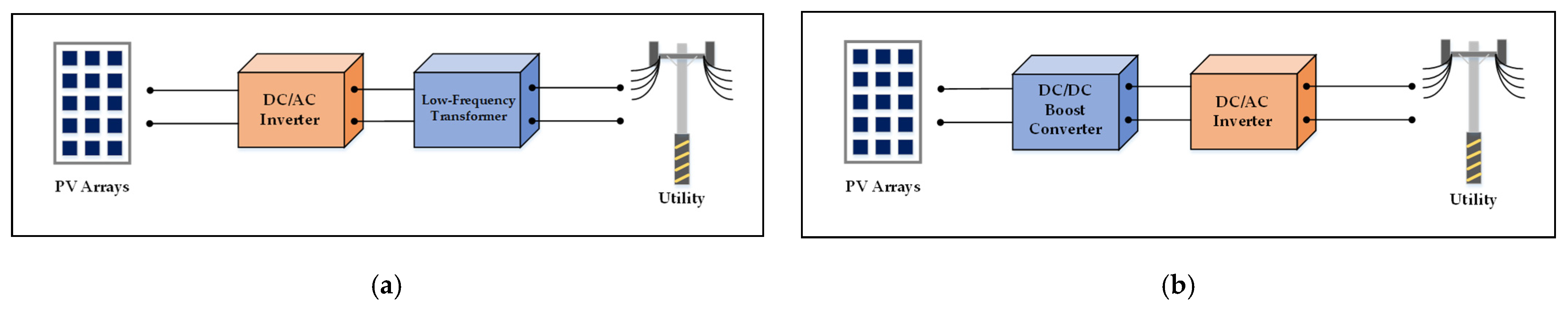
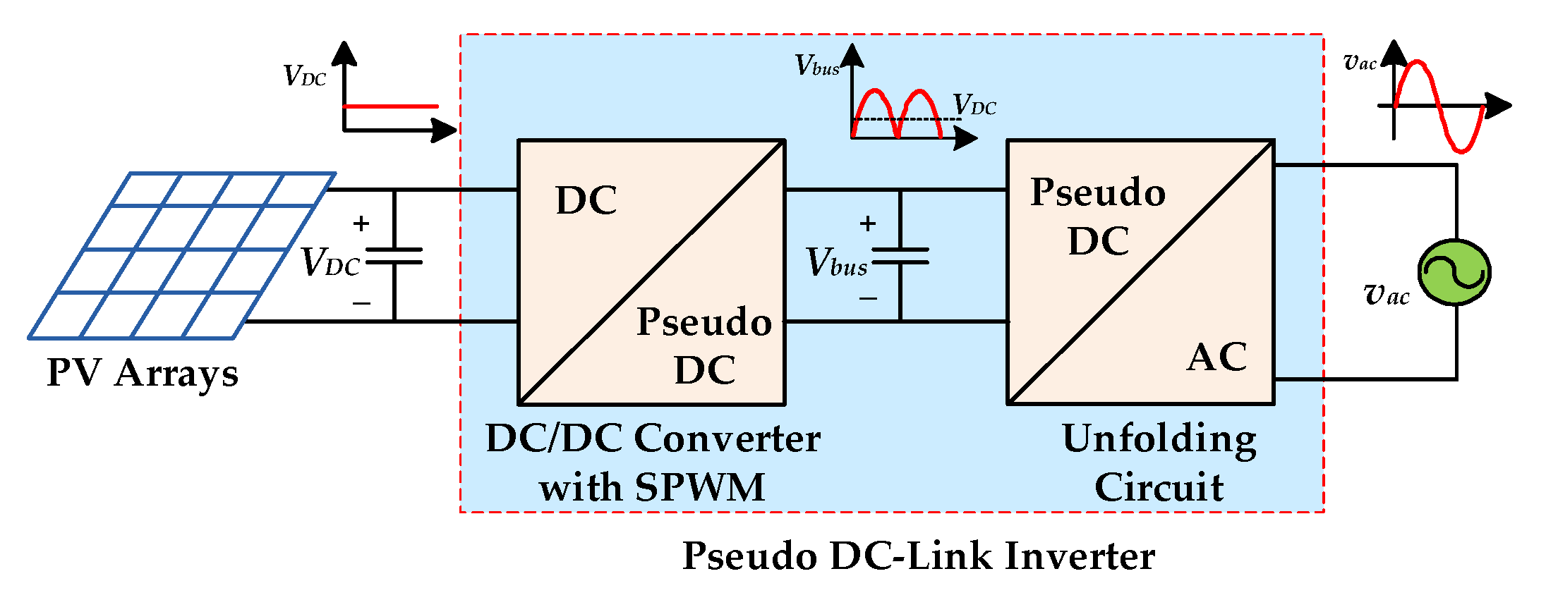
:1. Introduction
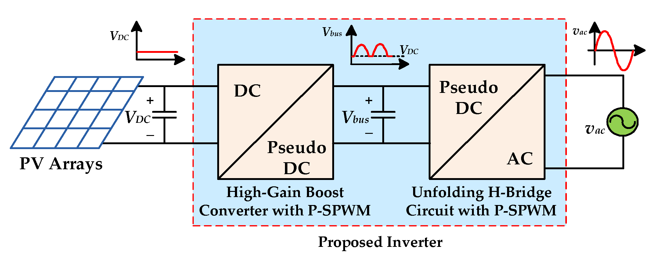
- Because the high-gain boost converter and the full-bridge unfolding circuit perform high-frequency switching at different times, only one energy processing stage is required to generate the sinusoidal output voltage, which can effectively improve the conversion efficiency.
- The full-bridge unfolding circuit is used to realize the step-down function so that additional series power switch is not required, which can reduce conduction losses.
- The proposed inverter has both step-up and step-down capabilities, making it suitable for applications with a wide range of input voltage variations.
2. Circuit Configuration
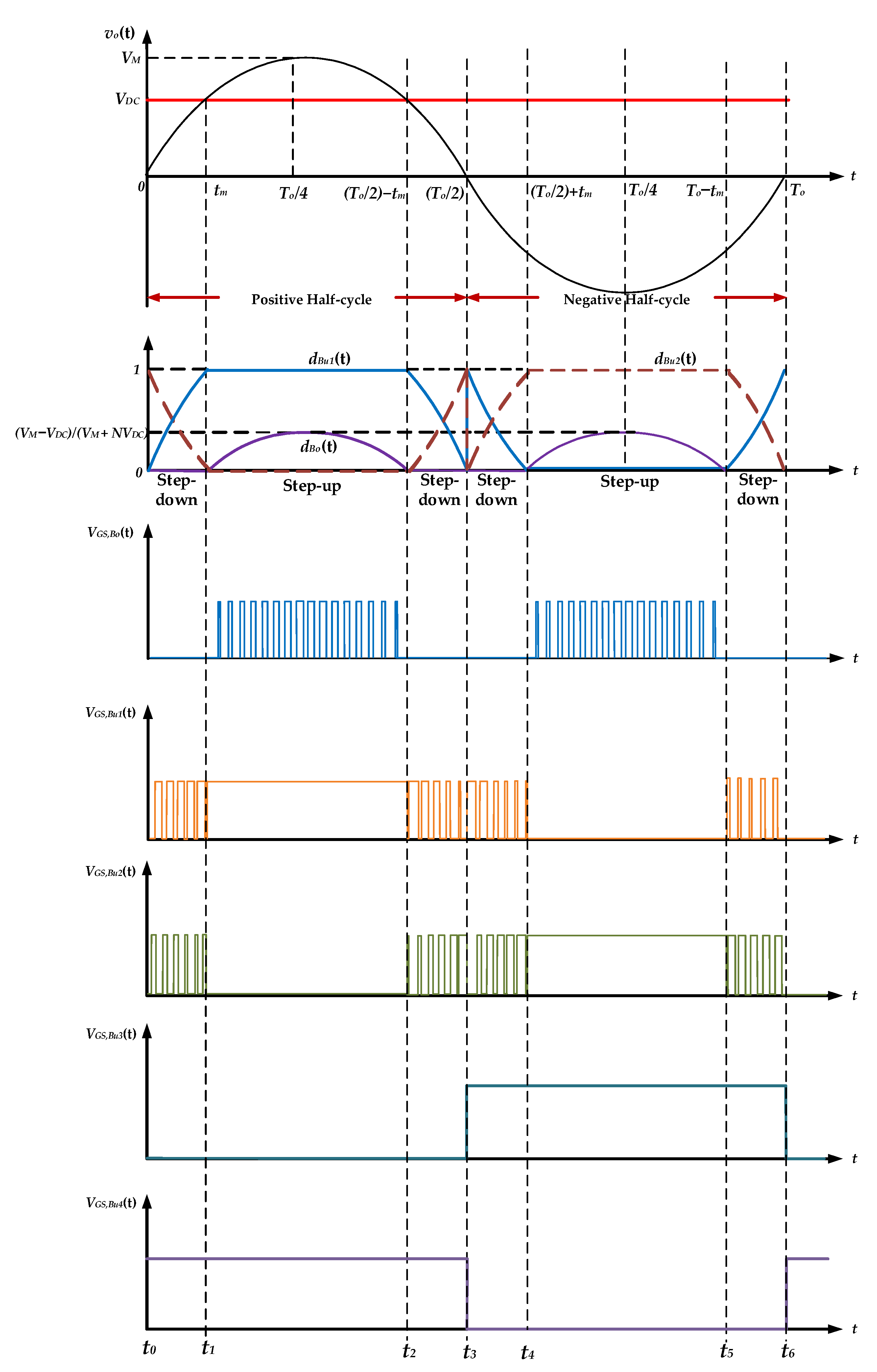
3. Operation Principles
- All circuit elements are ideal.
- The circuit operates in steady state.
- Inductor currents are continuous.
- The dead time of power switches is extremely short and can be ignored.
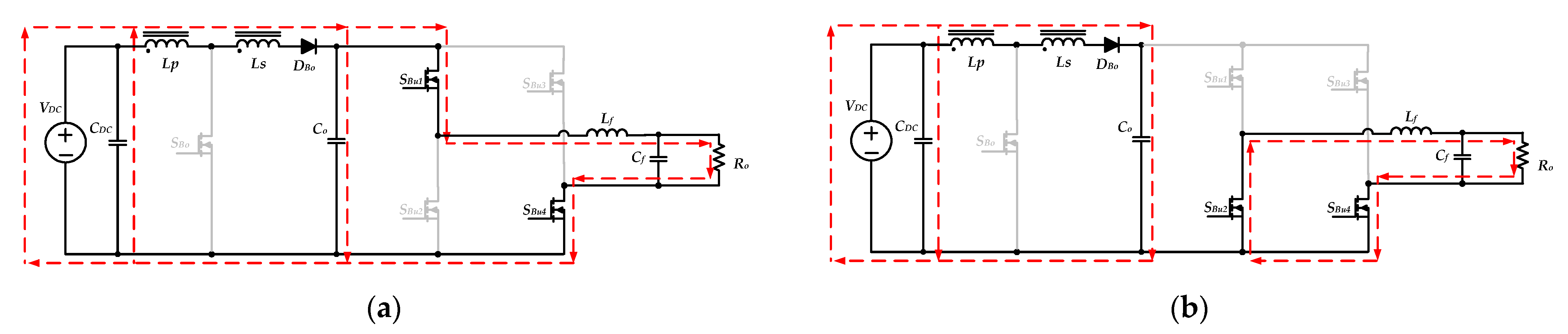
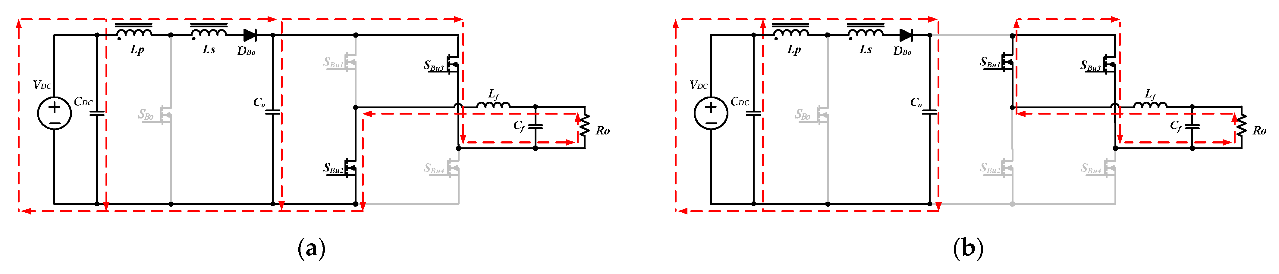
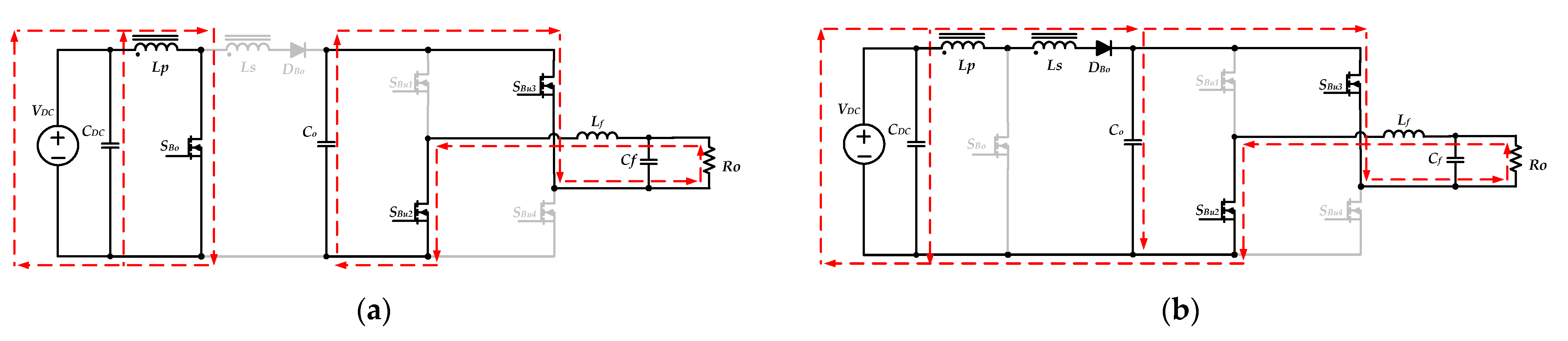
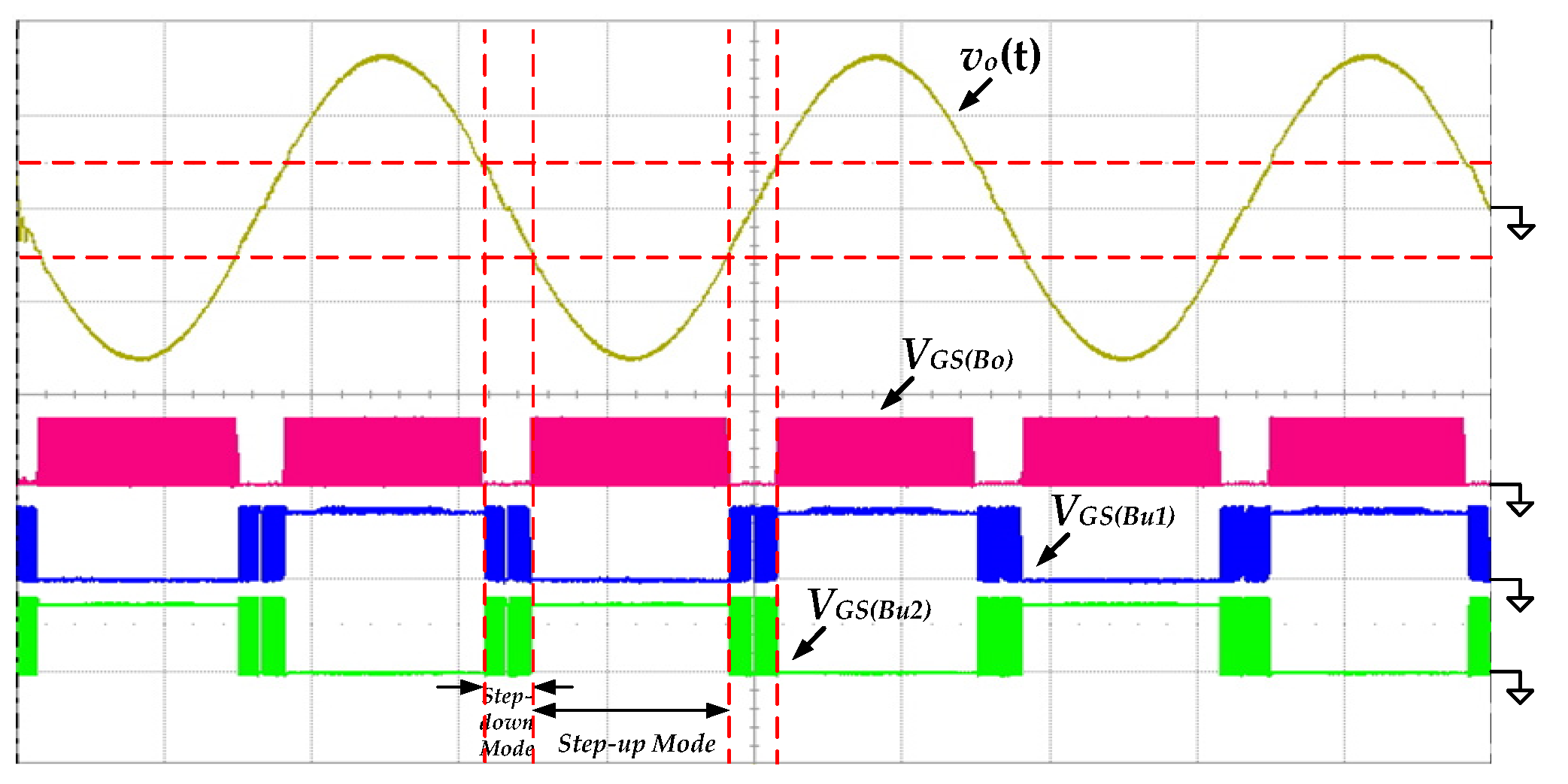
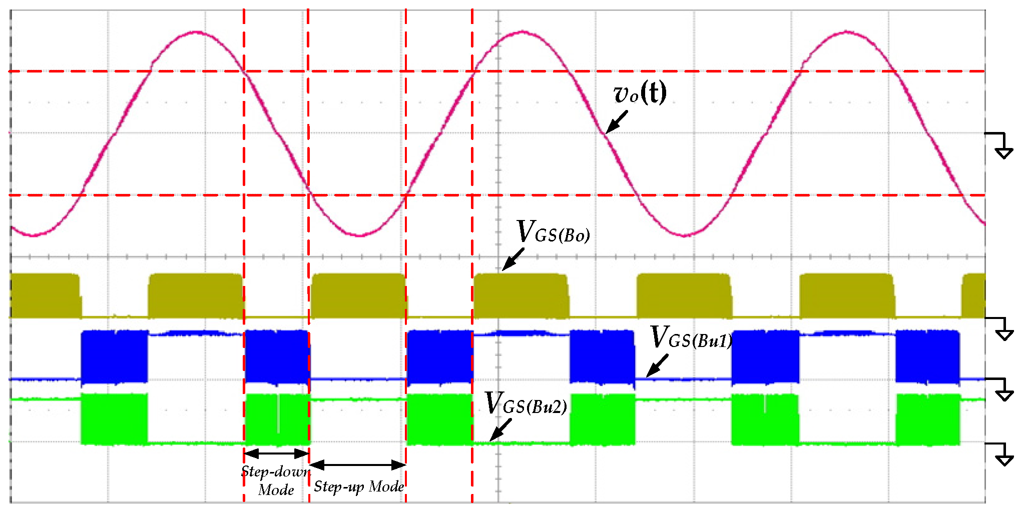
3.1. Step-Down Mode
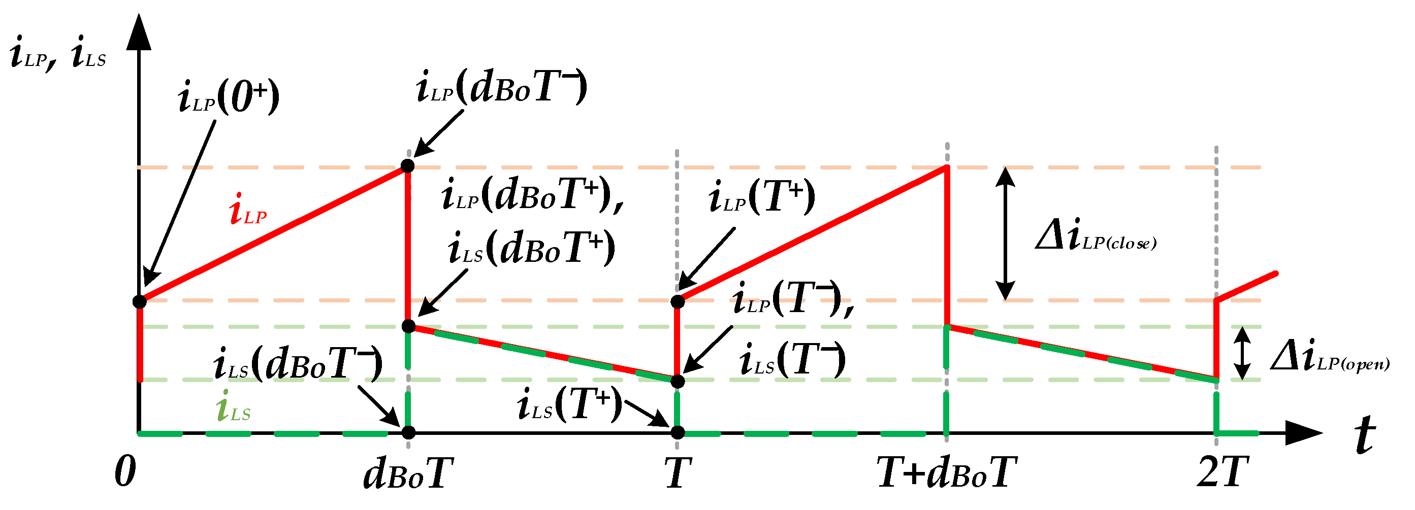
3.2. Step-Up Mode
4. Design Considerations
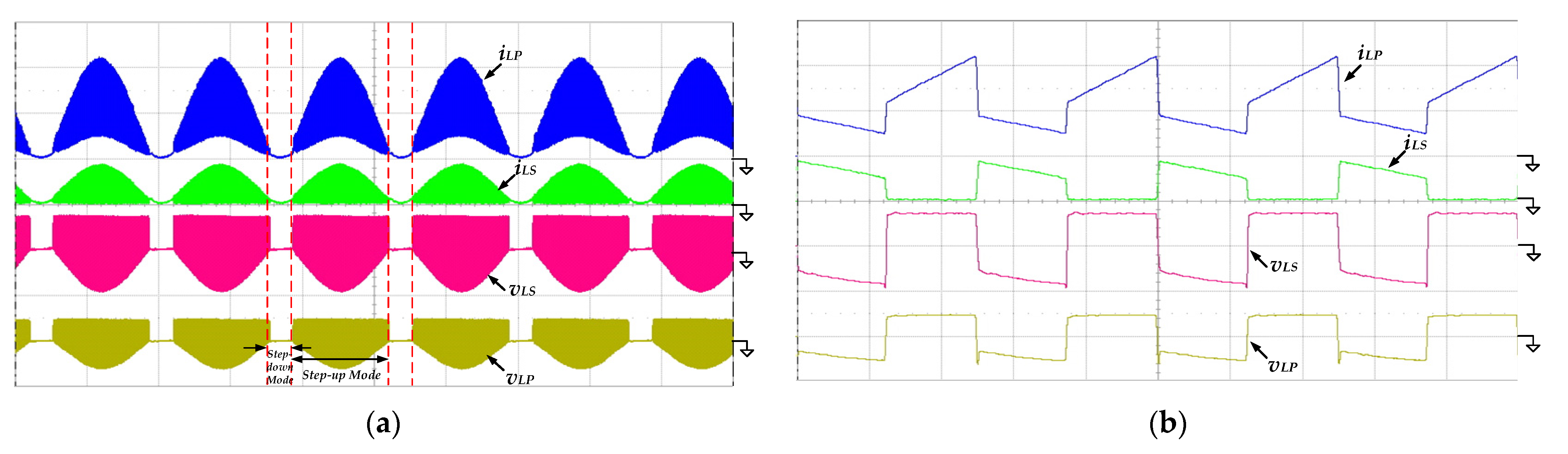
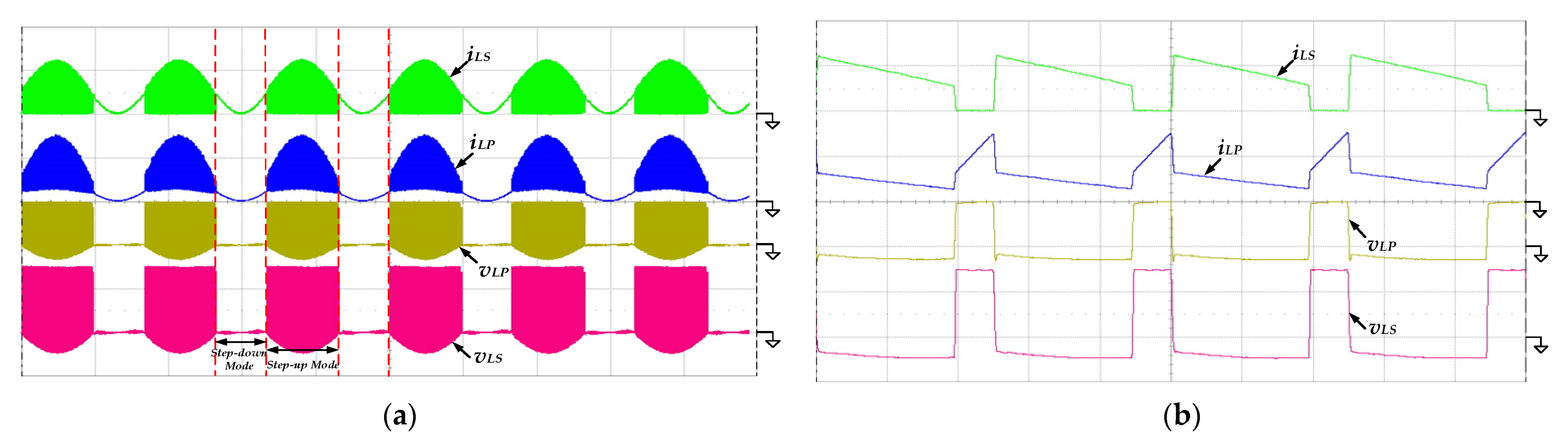
4.1. Boundary Condition of the Coupled Inductor
4.2. Voltage Stresses of the Power Components
4.3. Current Stresses of the Power Components
4.4. Selection of the Output Filter
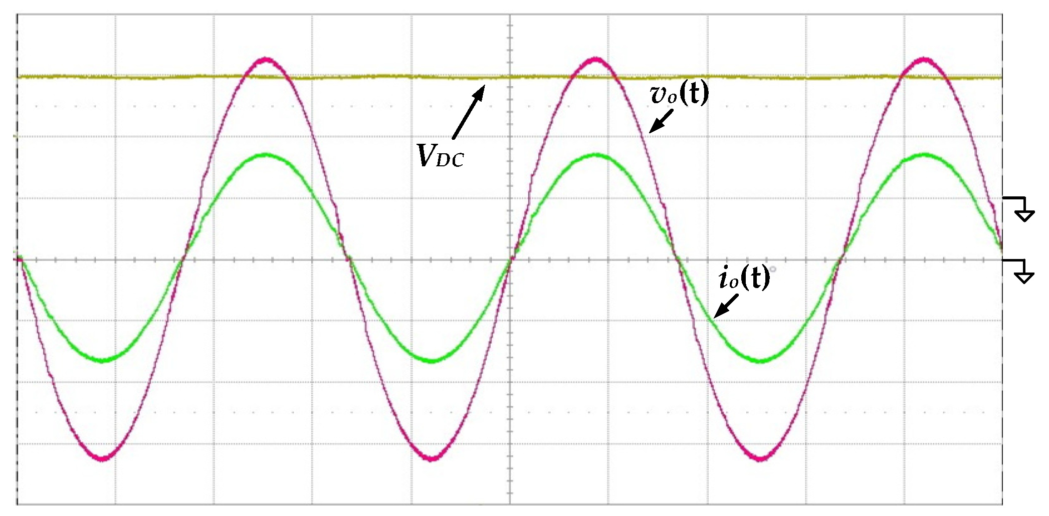
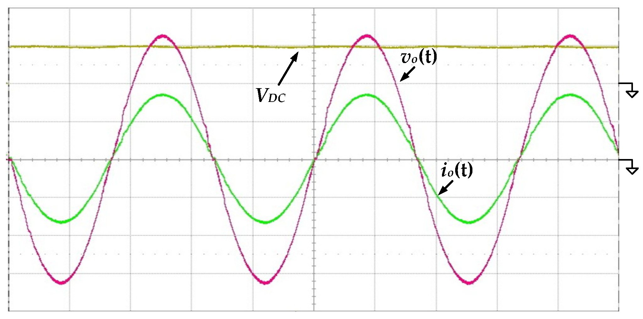
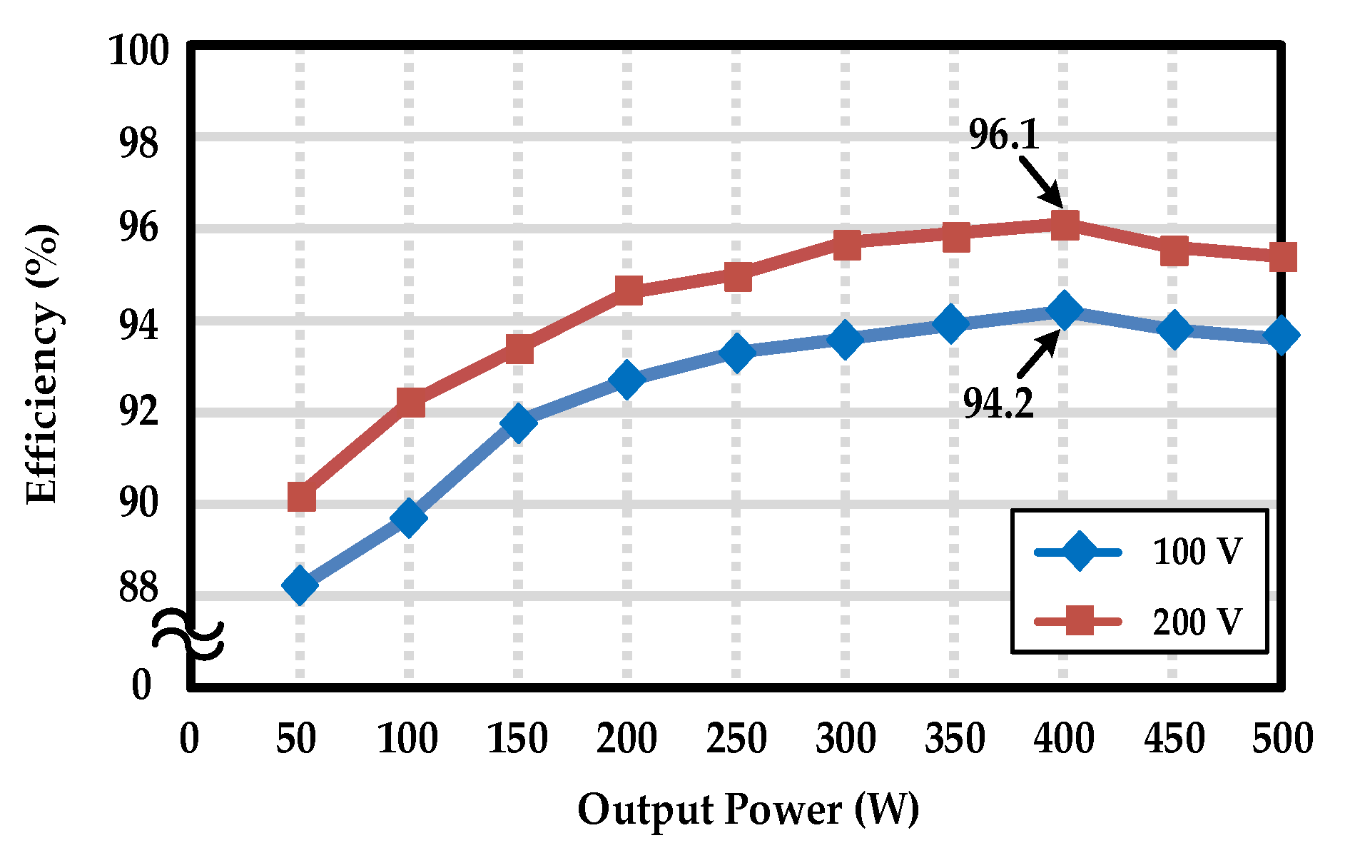
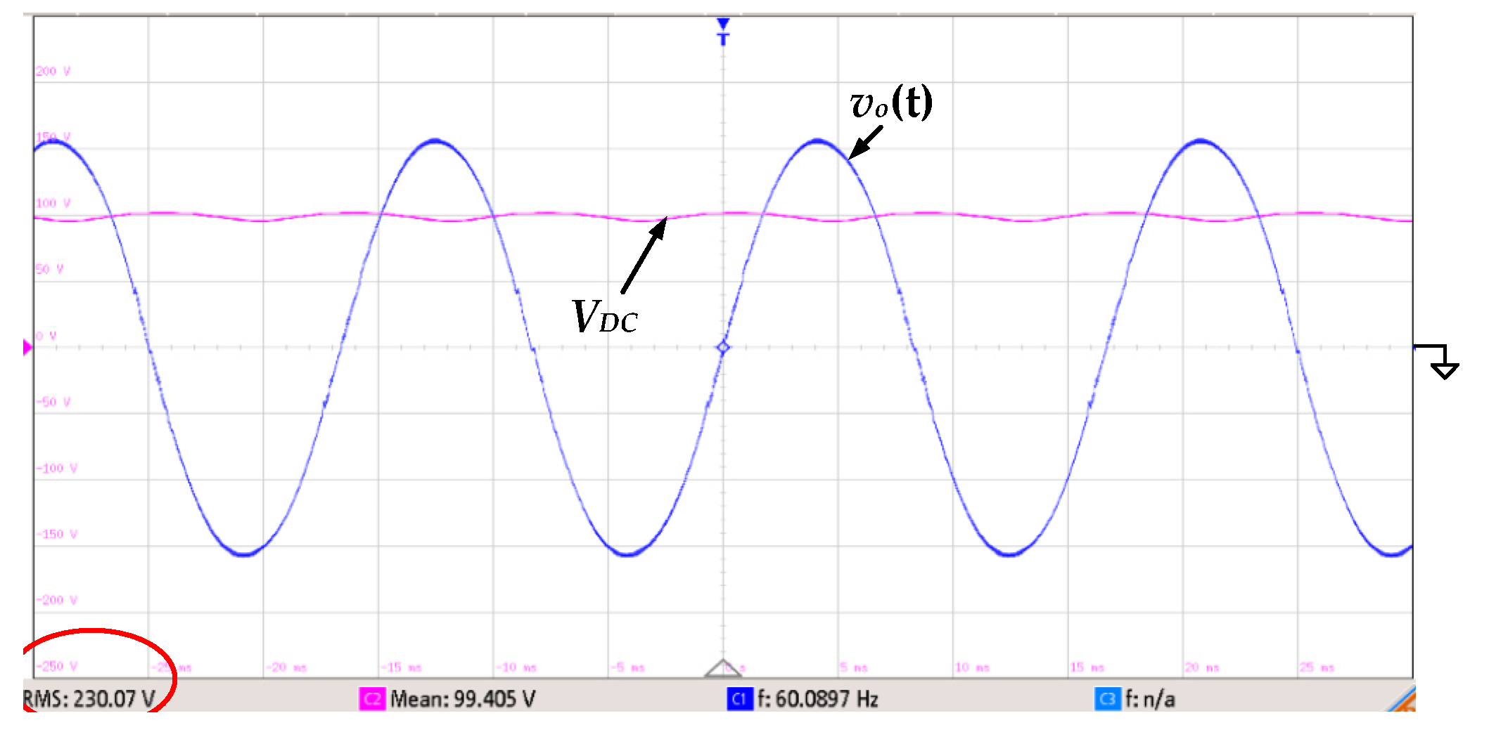
5. Experimental Results
6. Conclusions
Author Contributions
Funding
Acknowledgments
Conflicts of Interest
References
- Eftekharnejad, S.; Heydt, G.T.; Vittal, V. Optimal generation dispatch with high penetration of photovoltaic generation. IEEE Trans Sustain. Energy 2015, 6, 1013–1020. [Google Scholar] [CrossRef]
- Mehdiabadi, M.H.; Zhang, J.; Hedman, K.W. Wind power dispatch margin for flexible energy and reserve scheduling with increased wind generation. IEEE Trans Sustain. Energy 2015, 6, 1543–1552. [Google Scholar] [CrossRef]
- Hossain, M.S.; Jahid, A.; Islam, K.Z.; Rahman, M.F. Solar PV and biomass resources-based sustainable energy supply for off-grid cellular base stations. IEEE Access 2020, 8, 53817–53840. [Google Scholar] [CrossRef]
- Thang, T.V.; Ahmed, A.; Kim, C.-I.; Park, J.-H. Flexible system architecture of stand-alone PV power generation with energy storage device. IEEE Trans. Energy Convers. 2015, 30, 1386–1396. [Google Scholar] [CrossRef]
- Li, B.; Tian, X.; Zeng, H. A grid-connection control scheme of PV system with fluctuant reactive load. In Proceedings of the 2011 4th International Conference on Electric Utility Deregulation and Restructuring and Power Technologies (DRPT), Weihai, China, 6–9 July 2011; pp. 786–790. [Google Scholar]
- Jain, S.; Goyal, L. Current control methodology for PV in both standalone & grid connected mode. In Proceedings of the 2014 IEEE 6th India International Conference on Power Electronics (IICPE), Kurukshetra, India, 8–10 December 2014. [Google Scholar]
- Sangwongwanich, A.; Yang, Y.; Blaabjerg, F.; Sera, D. Delta power control strategy for multistring grid-connected PV inverters. IEEE Trans. Ind. Appl. 2017, 53, 3862–3870. [Google Scholar] [CrossRef]
- Kim, K.; Cha, H.; Kim, H.-G. A new single-phase switched-coupled-inductor dc-ac inverter for photovoltaic systems. IEEE Trans. Ind. Electron. 2017, 32, 5016–5022. [Google Scholar] [CrossRef]
- Hung, G.-K.; Chang, C.-C.; Chen, C.-L. Automatic phase-shift method for islanding detection of grid-connected photovoltaic inverters. IEEE Trans. Energy Convers. 2003, 18, 169–173. [Google Scholar] [CrossRef]
- Ardashir, J.F.; Sabahi, M.; Hosseini, S.H.; Blaabjerg, F.; Babaei, E.; Gharehpetian, G.B. A single-phase transformerless inverter with charge pump circuit concept for grid-tied PV applications. IEEE Trans. Ind. Electron. 2017, 64, 5403–5415. [Google Scholar] [CrossRef]
- Wang, C.M. A novel single-stage full-bridge buck-boost inverter. IEEE Trans. Power Electron. 2004, 19, 150–159. [Google Scholar] [CrossRef]
- Khan, A.A.; Cha, H. Dual-buck-structured high-reliability and high efficiency single-stage buck–boost inverters. IEEE Trans. Ind. Electron. 2018, 65, 3176–3187. [Google Scholar] [CrossRef]
- Tang, Y.; Bai, Y.; Kan, J.; Xu, F. Improved dual boost inverter with half cycle modulation. IEEE Trans. Power Electron. 2017, 32, 7543–7552. [Google Scholar] [CrossRef]
- Saha, S.; Sundarsingh, V.P. Novel grid-connected photovoltaic inverter. Proc. Inst. Elect. Eng. 1996, 143, 219–224. [Google Scholar] [CrossRef]
- Zhao, Z.; Xu, M.; Chen, Q.; Lai, J.-S.; Cho, Y. Derivation, analysis, and implementation of a boost–buck converter-based high-efficiency PV inverter. IEEE Trans. Power Electron. 2012, 27, 1304–1313. [Google Scholar] [CrossRef]
- Chang, C.-H.; Cheng, C.-A.; Chang, E.-C.; Cheng, H.-L. Design and implementation of a two-switch buck-boost typed inverter with universal and high-efficiency features. In Proceedings of the 9th International Conference on Power Electronics and ECCE Asia (ICPE-ECCE Asia), Seoul, Korea, 1–5 June 2015; pp. 2737–2743. [Google Scholar]
- Tamyurek, B.; Kirimer, B. An interleaved high-power flyback inverter for photovoltaic applications. IEEE Trans. Power Electron. 2015, 30, 3228–3241. [Google Scholar] [CrossRef]
- Chang, C.-H.; Cheng, C.-A.; Cheng, H.-L.; Wu, Y.-T. An active-clamp forward inverter featuring soft switching and electrical isolation. Appl. Sci. 2020, 10, 4220. [Google Scholar] [CrossRef]
- Ajami, A.; Ardi, H.; Farakhor, A. A novel high step-up DC/DC converter based on integrating coupled inductor and switched-capacitor techniques for renewable energy applications. IEEE Trans. Power Electron. 2015, 30, 4255–4263. [Google Scholar] [CrossRef]
- Akhormeh, A.R.N.; Abbaszadeh, K.; Moradzadeh, M.; Shahirinia, A. High-gain bidirectional quadratic DC–DC converter based on coupled inductor with current ripple reduction capability. IEEE Trans. Ind. Electron. 2021, 68, 7826–7837. [Google Scholar] [CrossRef]


| Element | Positive Half-Cycle (0 < t < To/2) | Negative Half-Cycle (To/2 < t < To) | ||
|---|---|---|---|---|
| Step-Down Mode | Step-Up Mode | Step-Down Mode | Step-Up Mode | |
| SBu1 | Switching with dBu1(t) | Always on | Switching with (1 − dBu1(t)) | Always off |
| SBu2 | Switching with (1 − dBu1(t)) | Always off | Switching with dBu1(t) | Always on |
| SBu3 | Always off | Always off | Always on | Always on |
| SBu4 | Always on | Always on | Always off | Always off |
| SBo | Always off | Switching with dBo(t) | Always off | Switching with dBo(t) |
| DBo | Always on | Switching with (1 − dBo(t)) | Always on | Switching with (1 − dBo(t)) |
| Electrical Specifications | |
|---|---|
| Input voltage, VDC | 100–200 (V) |
| Output voltage, vo | 220 (Vrms) |
| Line frequency, fo | 60 (Hz) |
| Output power, Po | 500 (W) |
| Switching frequency, f | 20 (kHz) |
| Switching period, T | 50 (μs) |
| Component Parameters | |
|---|---|
| MOSEET, SBo | SPW47N60C3 (650 V/47 A) |
| MOSEETs, SBu1, SBu2, SBu3 and SBu4 | IRFP460 (500 V/20 A) |
| Diode, DBo | C4D10120A (1200 V/14 A) |
| Turn Ratio, N | 1.5 |
| Primary Inductance, LP | 200 μH |
| Secondary Inductance, LS | 450 μH |
| Capacitor, Co | 1 μF |
| Inductor, Lf | 1 mH |
| Capacitor, Cf | 1 μF |
| Harmonic | 100 V | 200 V |
|---|---|---|
| T.H.D. | 1.73% | 1.13% |
| 3rd Harmonic | 1.57% | 0.87% |
| 5th Harmonic | 0.36% | 0.29% |
| 7th Harmonic | 0.24% | 0.33% |
| 9th Harmonic | 0.11% | 0.17% |
| 11th Harmonic | 0.07% | 0.12% |
Publisher’s Note: MDPI stays neutral with regard to jurisdictional claims in published maps and institutional affiliations. |
© 2022 by the authors. Licensee MDPI, Basel, Switzerland. This article is an open access article distributed under the terms and conditions of the Creative Commons Attribution (CC BY) license (https://creativecommons.org/licenses/by/4.0/).
Share and Cite
Chang, C.-H.; Cheng, C.-A.; Cheng, H.-L.; Chang, E.-C. A High-Gain and High-Efficiency Photovoltaic Grid-Connected Inverter with Magnetic Coupling. Micromachines 2022, 13, 1568. https://doi.org/10.3390/mi13101568
Chang C-H, Cheng C-A, Cheng H-L, Chang E-C. A High-Gain and High-Efficiency Photovoltaic Grid-Connected Inverter with Magnetic Coupling. Micromachines. 2022; 13(10):1568. https://doi.org/10.3390/mi13101568
Chicago/Turabian StyleChang, Chien-Hsuan, Chun-An Cheng, Hung-Liang Cheng, and En-Chih Chang. 2022. "A High-Gain and High-Efficiency Photovoltaic Grid-Connected Inverter with Magnetic Coupling" Micromachines 13, no. 10: 1568. https://doi.org/10.3390/mi13101568