
Low-Stress and Optimum Design of Boost Converter for Renewable Energy Systems

 , ,
, ,
Abstract
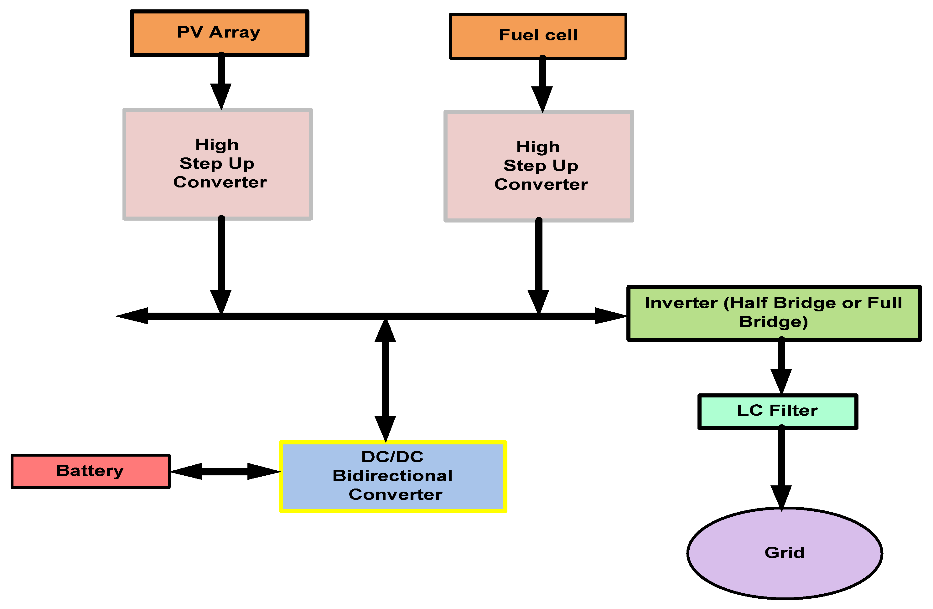
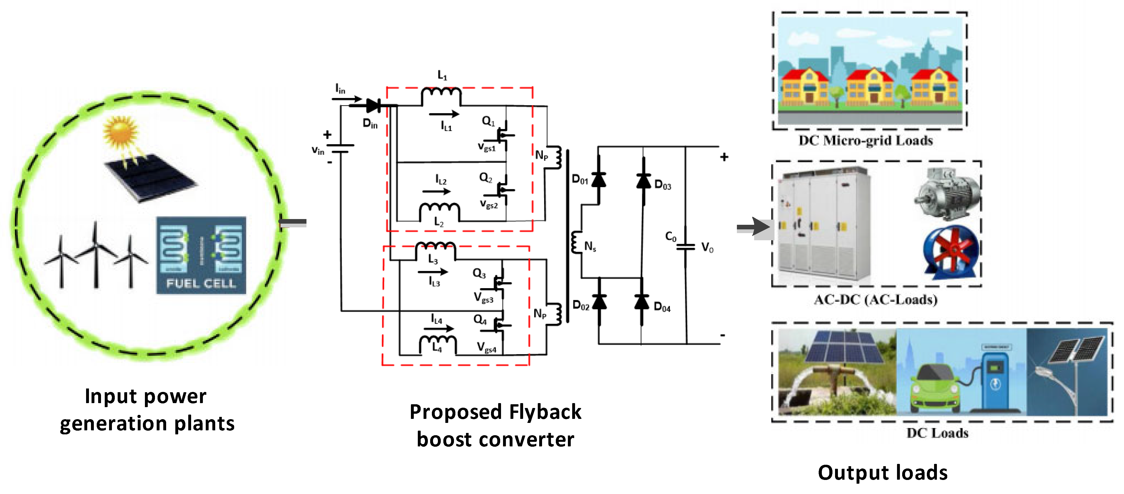
:1. Introduction
Related Work
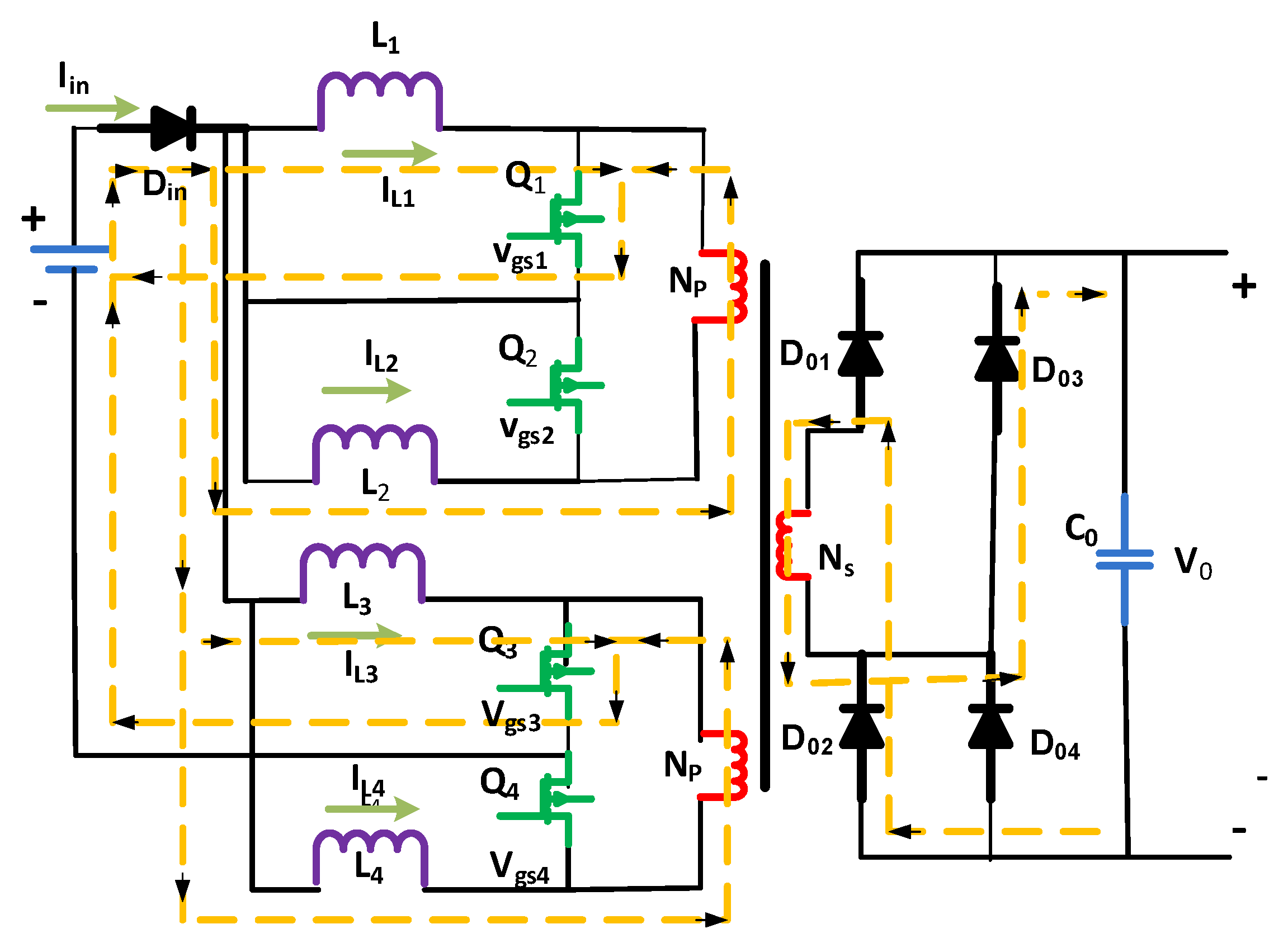
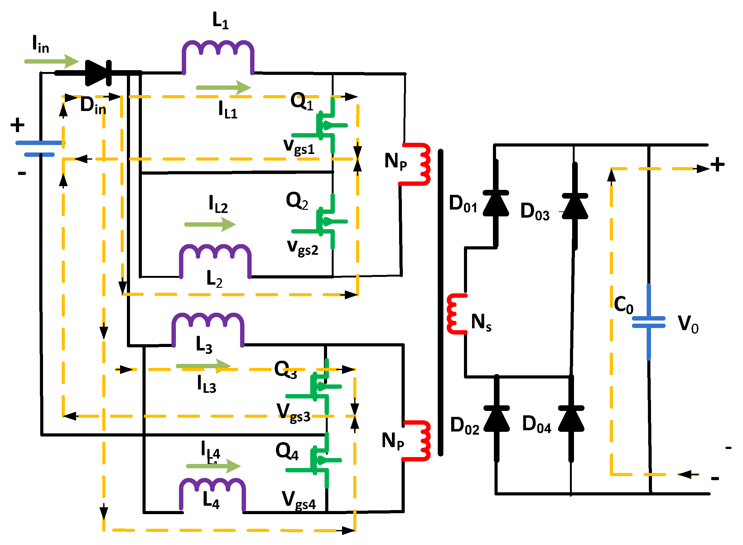
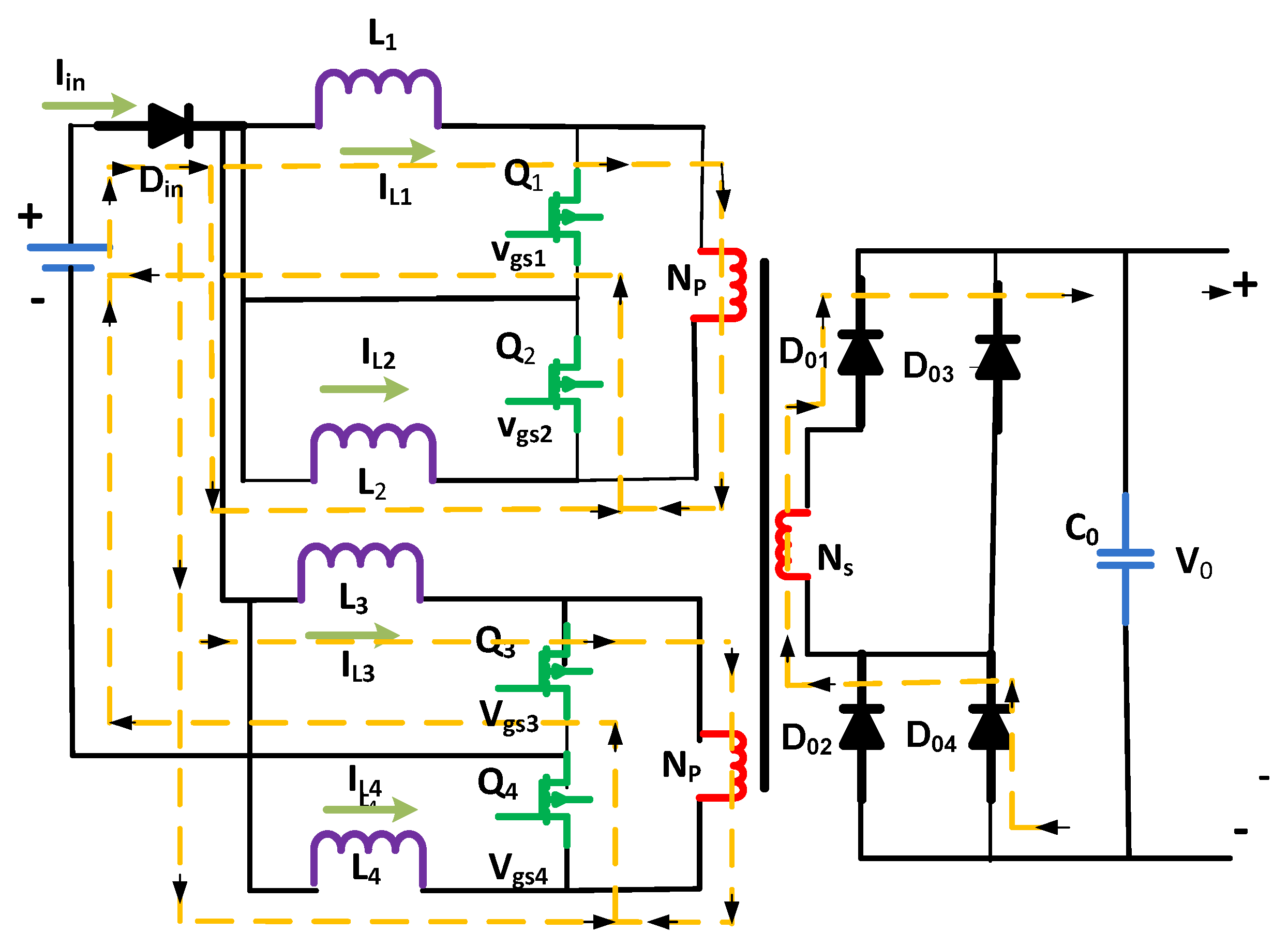
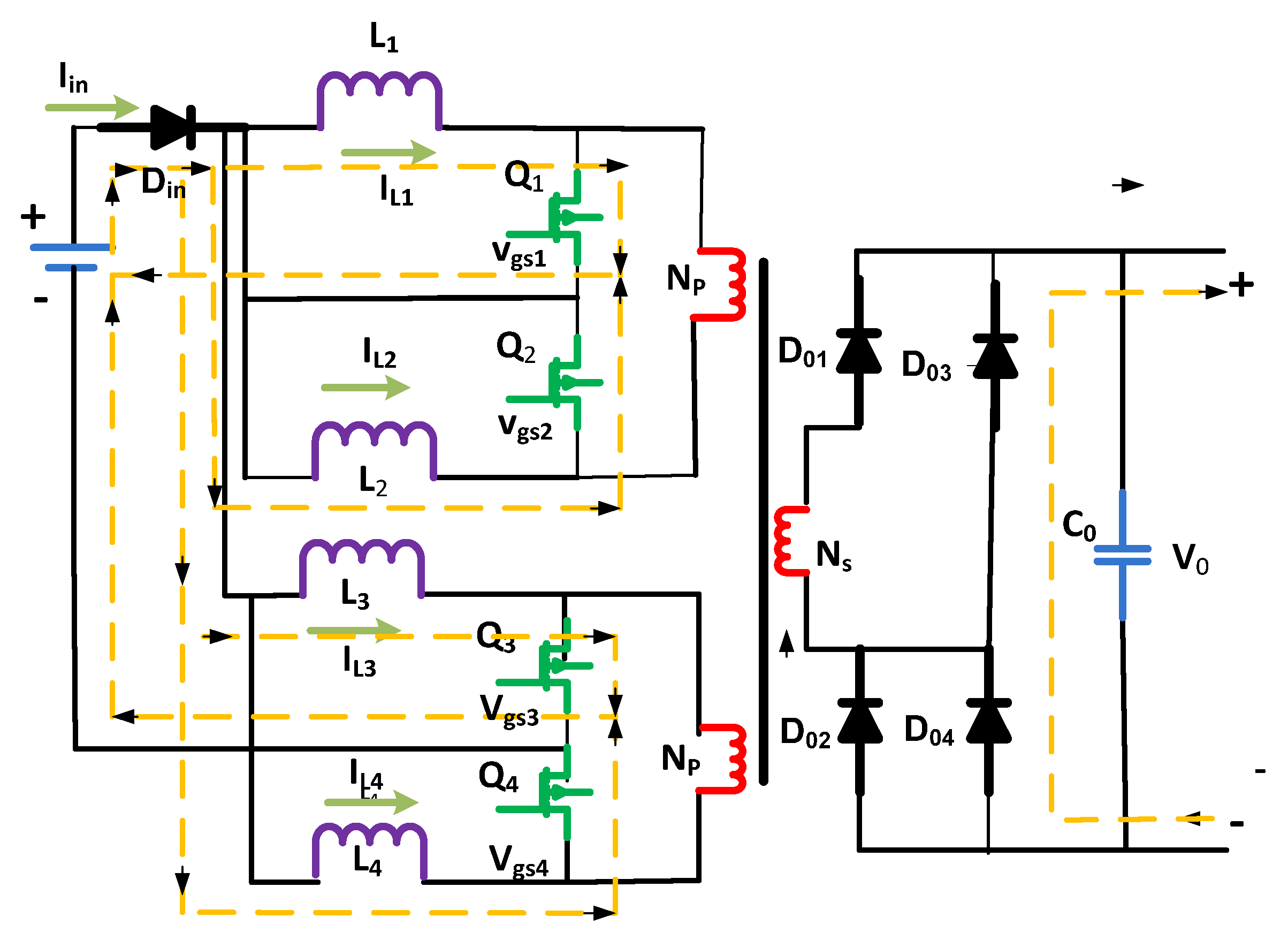
2. Proposed and Analytical Modeling
2.1. First Mode (t0–t1)
2.2. Second Mode (t1–t2)
2.3. Third Mode (t2–t3)
2.4. Fourth Mode (t3–t4)
3. Current and Voltage Stresses of the Switches
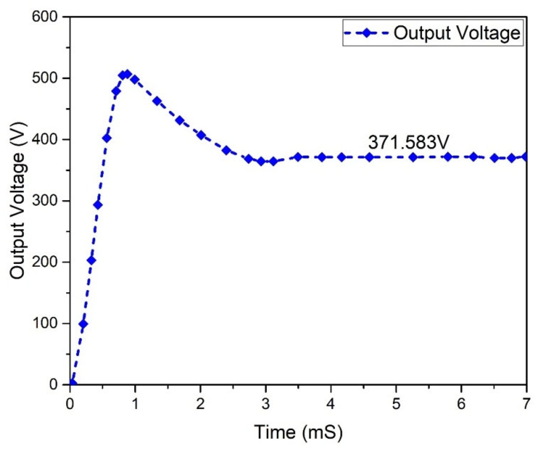
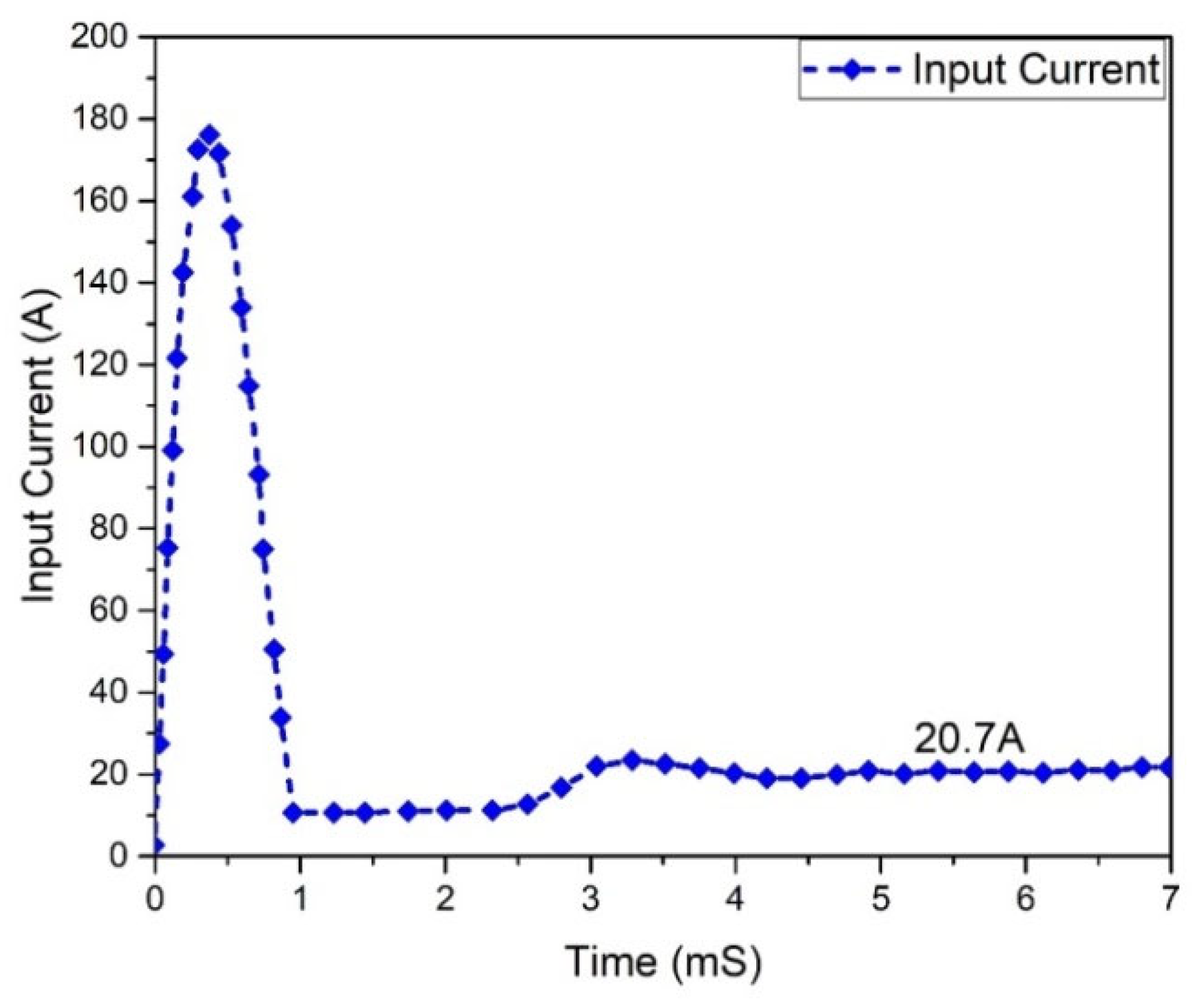
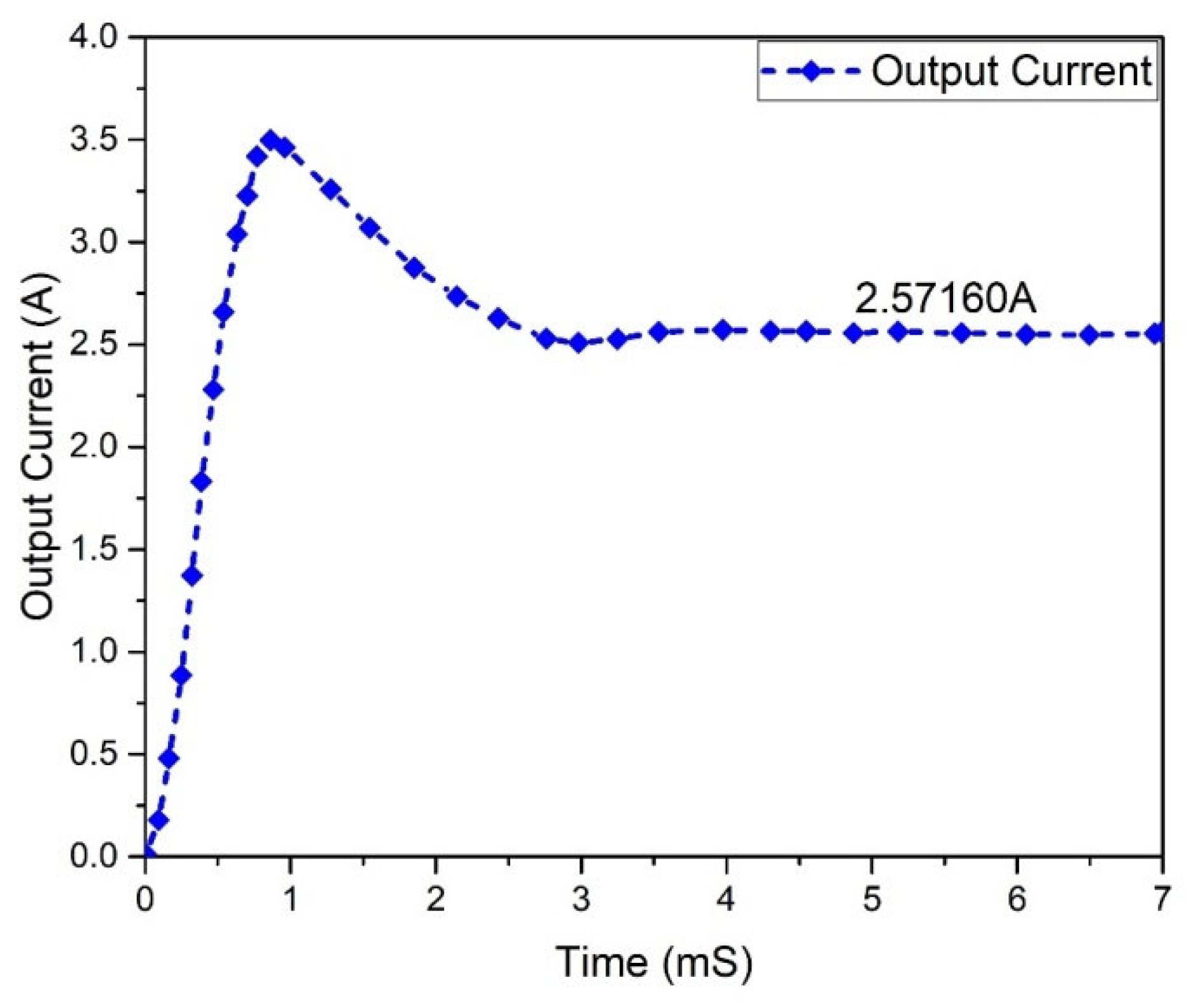
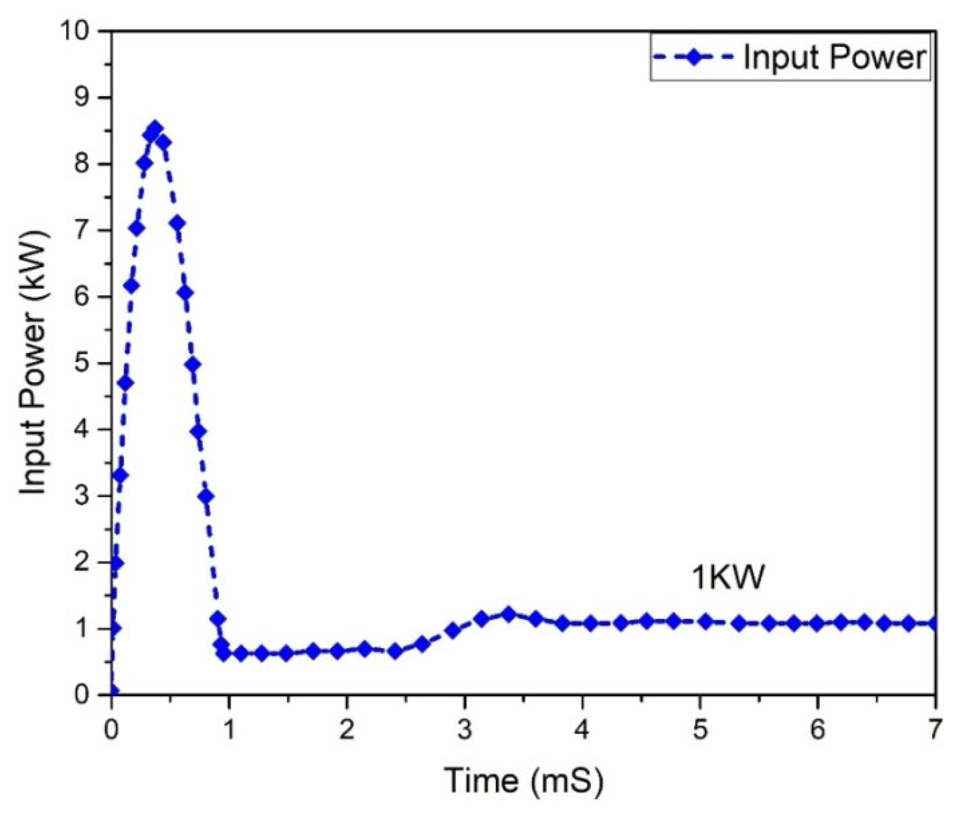
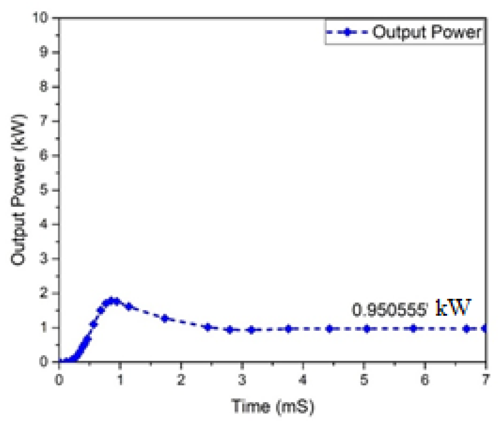
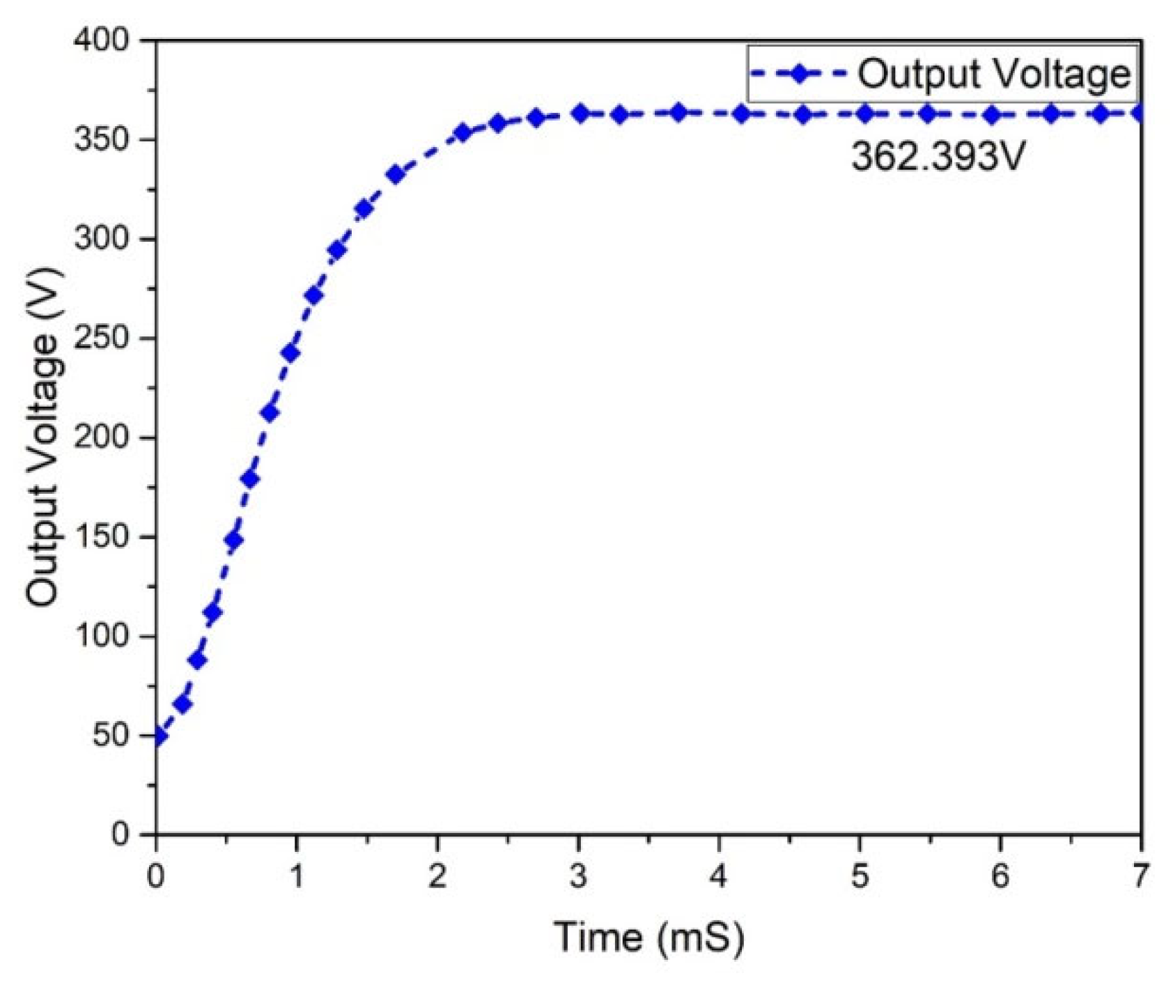
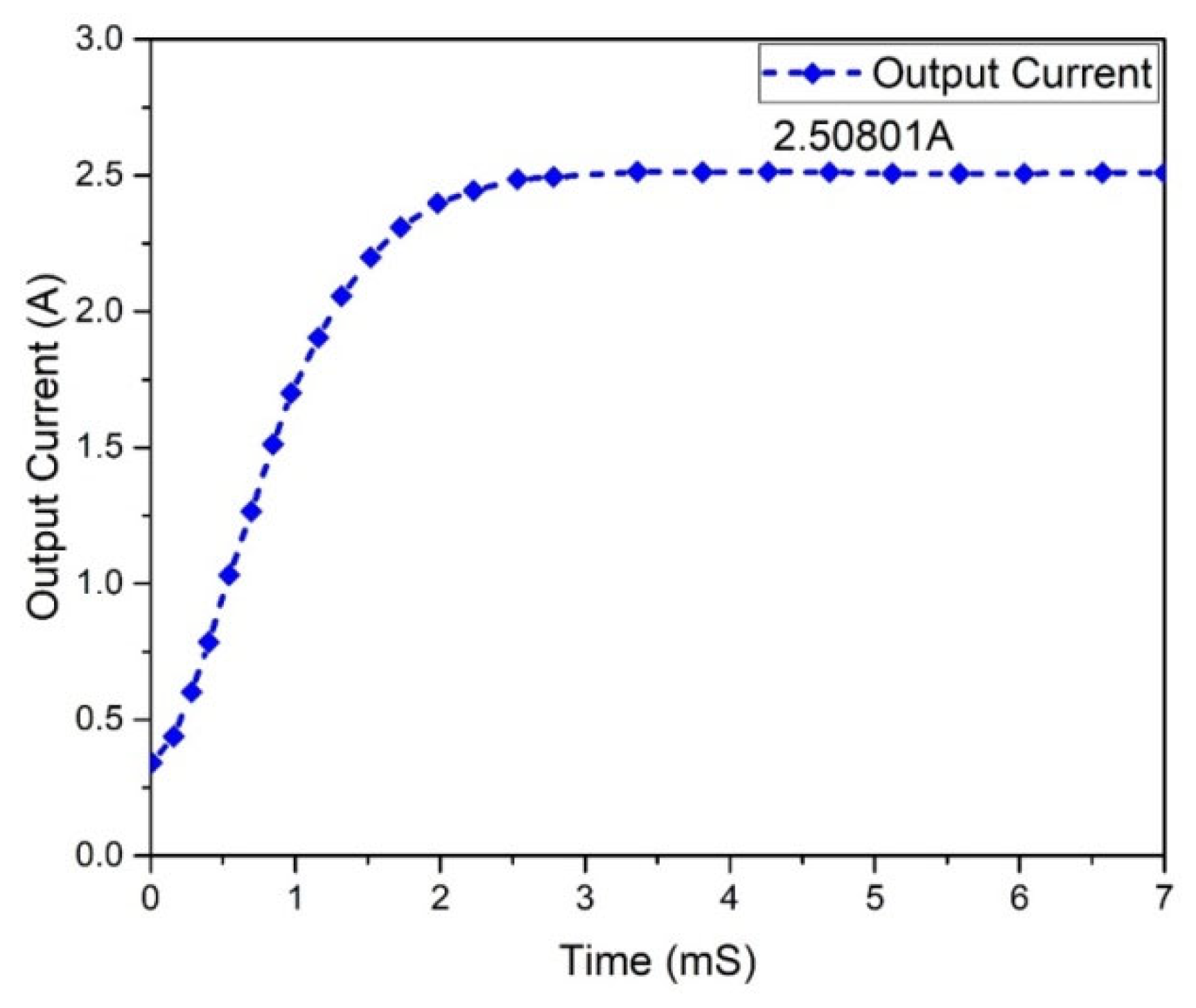
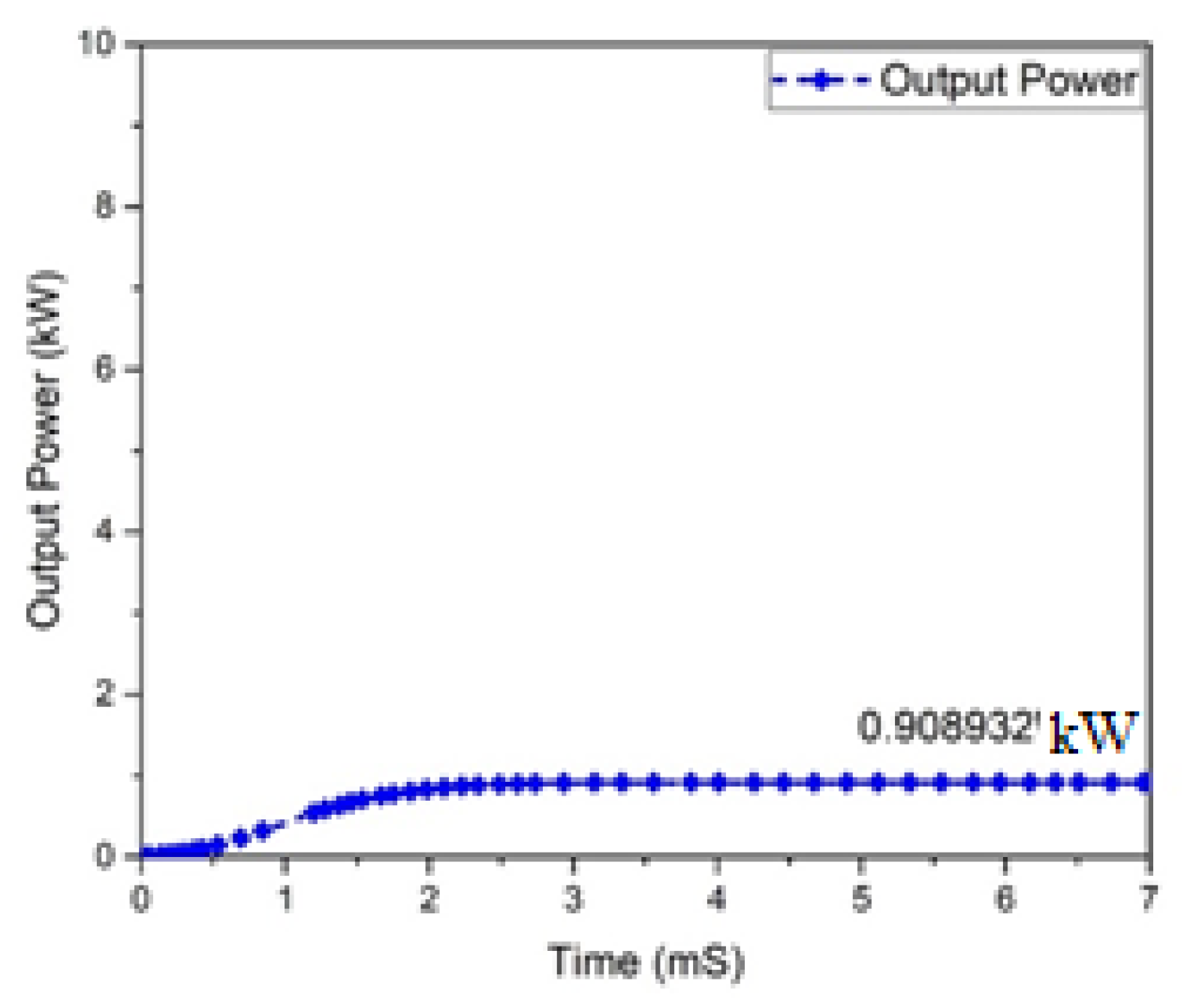
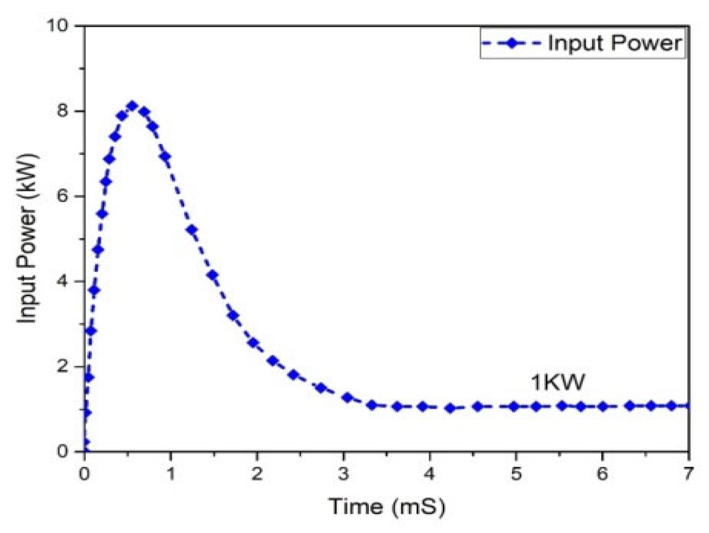
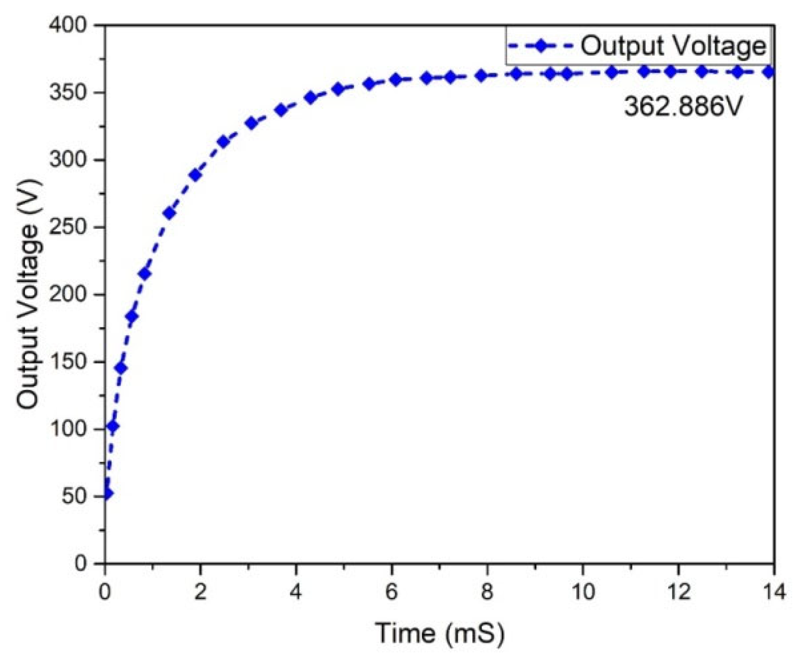
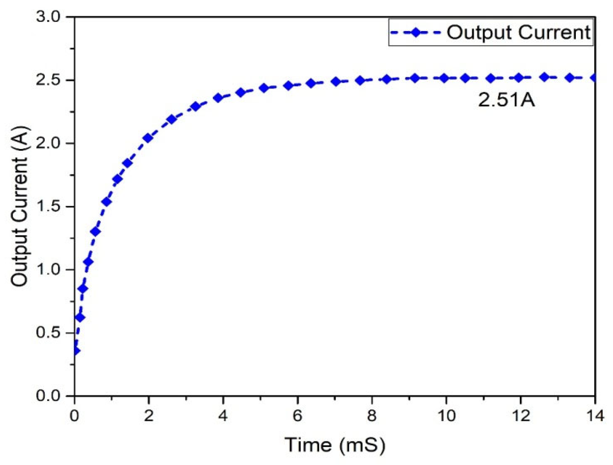
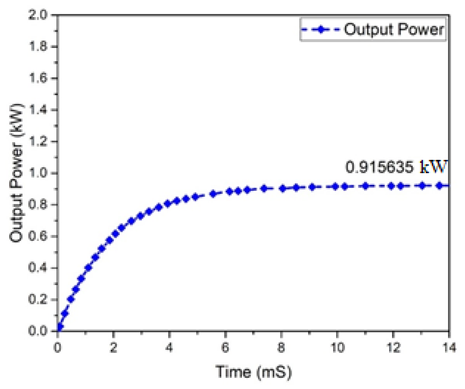
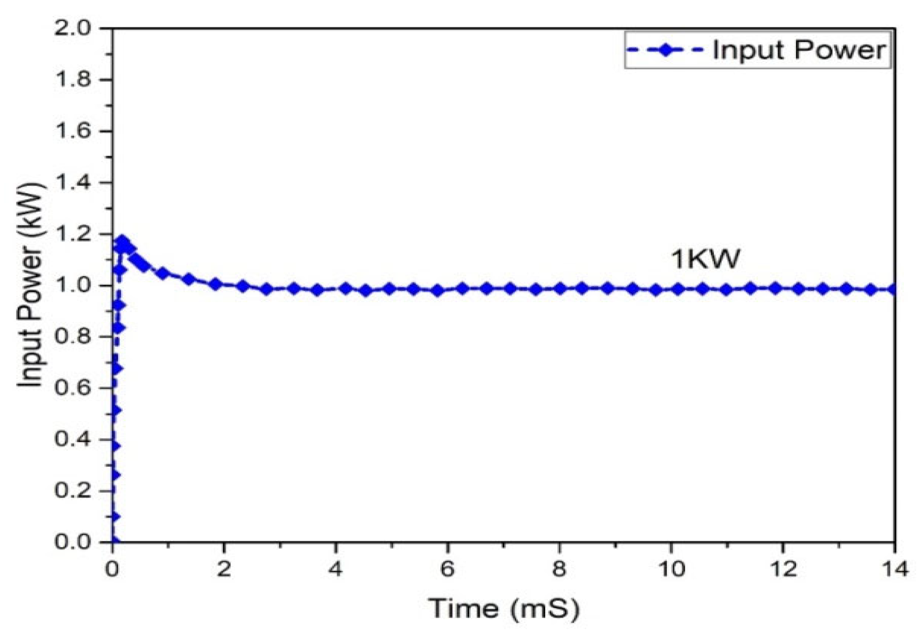
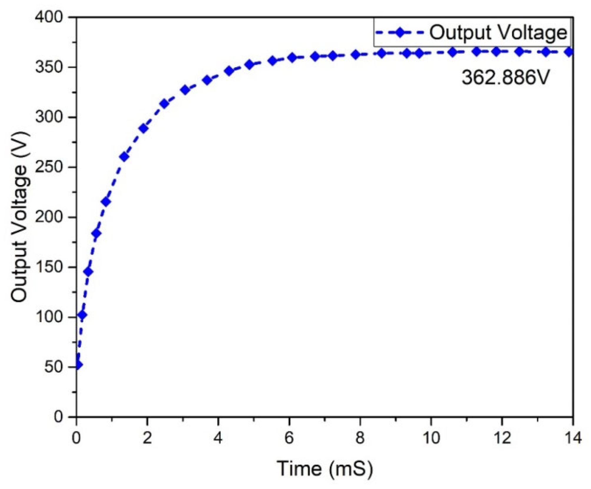
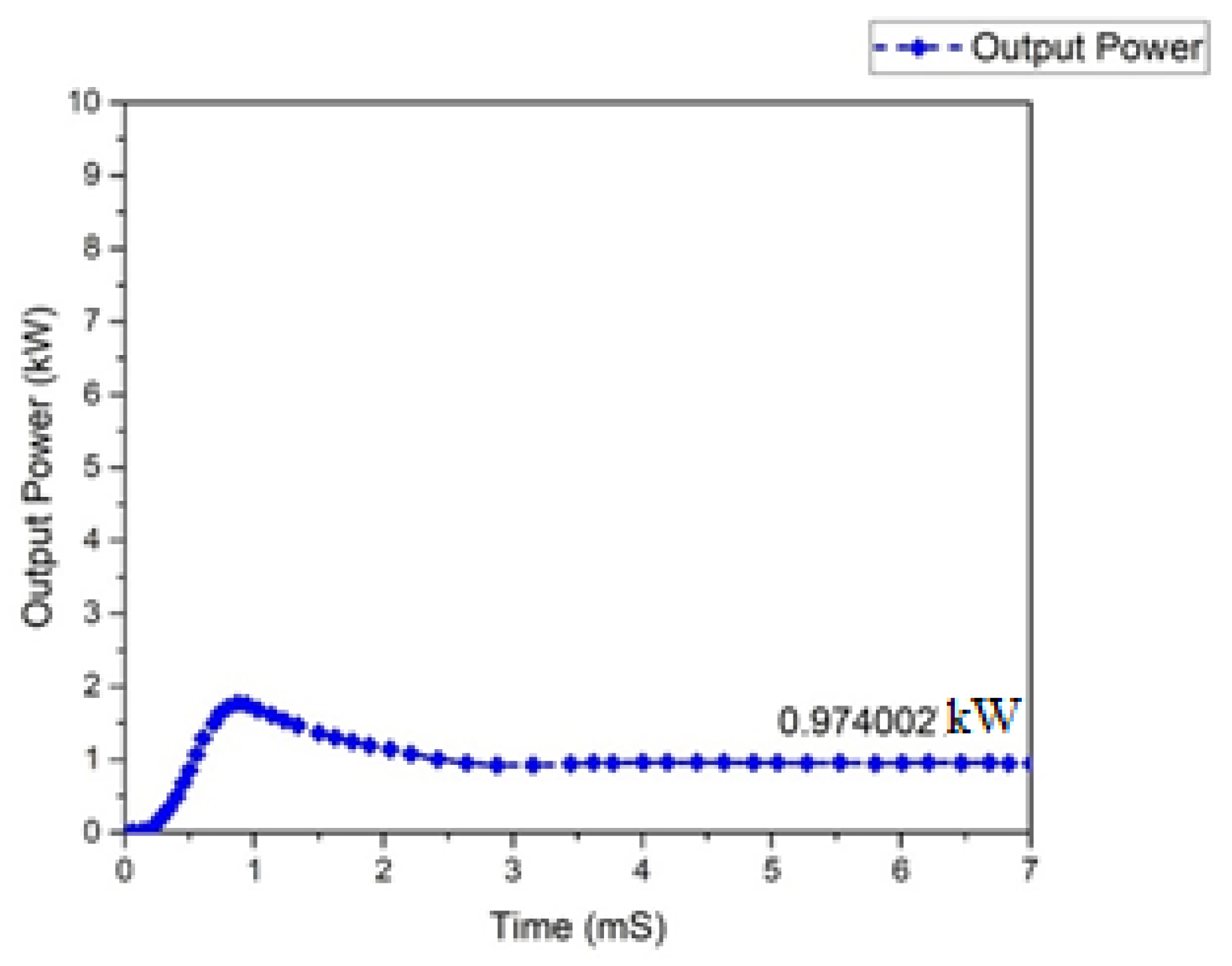
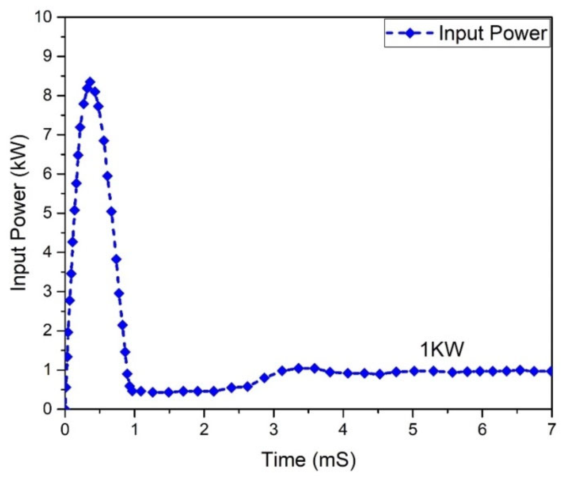
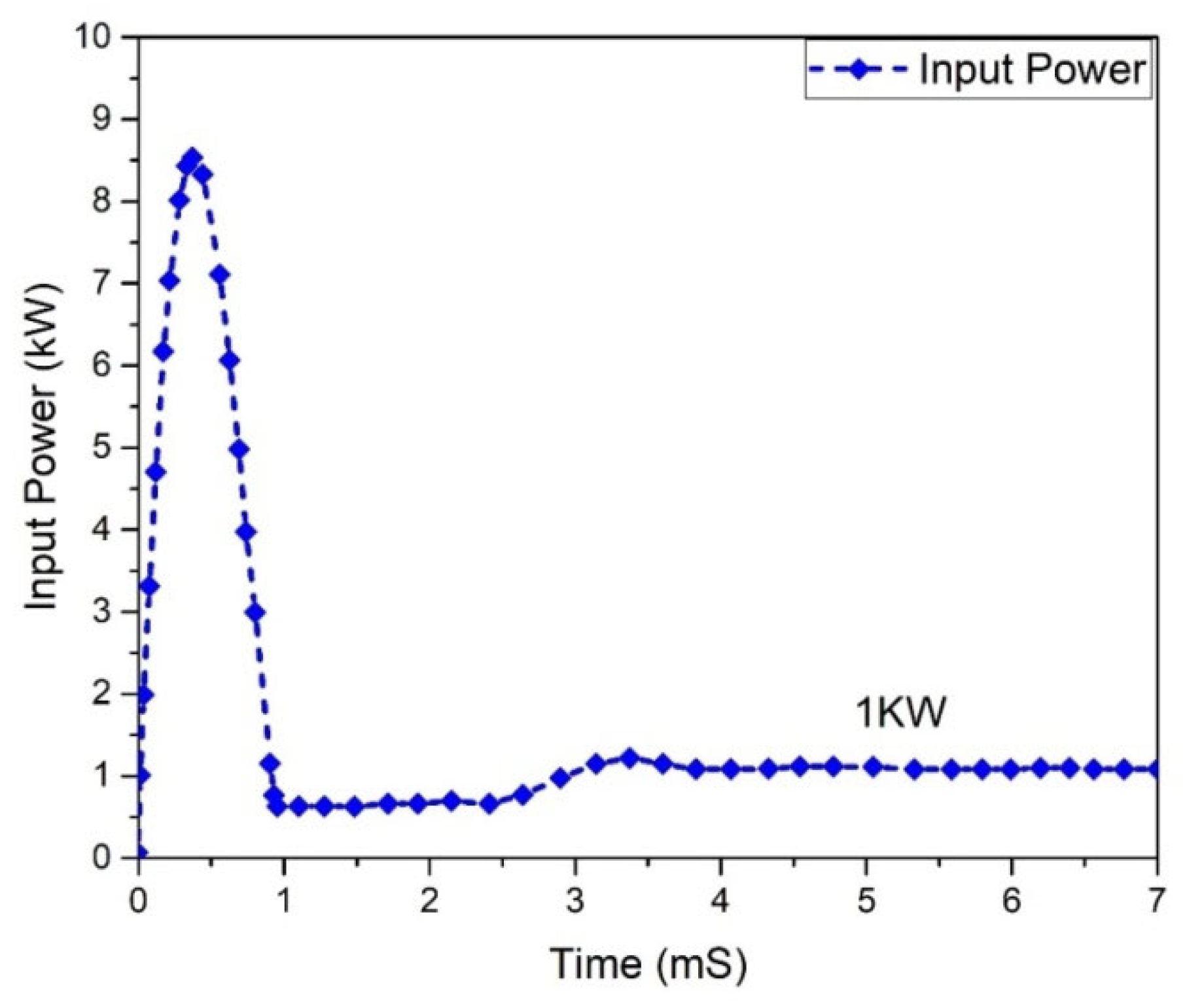
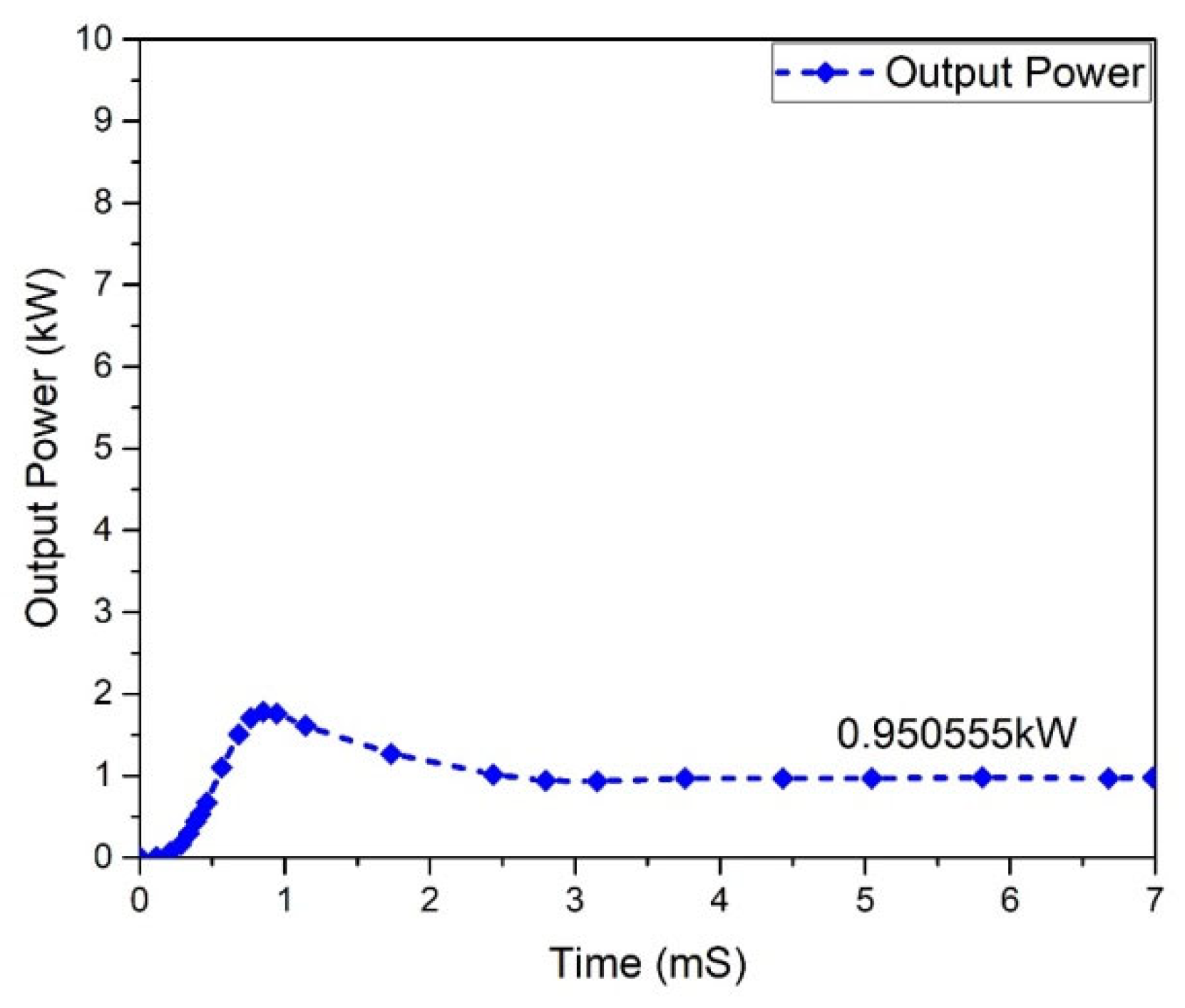
4. Results and Discussions
5. Conclusions
Author Contributions
Funding
Institutional Review Board Statement
Informed Consent Statement
Data Availability Statement
Conflicts of Interest
References
- Islam, M.S.; Jahid, A.; Islam, A.S.M.T.; Sharif; Sadath, M.A.; Monju, M.K.H. Renewable energy aware cost assessment for green data center with hybrid energy sources. In Proceedings of the 1st International Conference on Robotics, Electrical and Signal Processing Techniques, ICREST 2019, Dhaka, Bangladesh, 10–12 January 2019; pp. 120–125. [Google Scholar] [CrossRef]
- Miao, S.; Wang, F.; Ma, X. A New Transformerless Buck-Boost Converter With Positive Output Voltage. IEEE Trans. Ind. Electron. 2016, 63, 2965–2975. [Google Scholar] [CrossRef]
- Haseeb, I.; Armghan, A.; Khan, W.; Alenezi, F.; Alnaim, N.; Ali, F.; Muhammad, F.; Albogamy, F.R.; Ullah, N. Solar Power System Assessments Using ANN and Hybrid Boost Converter Based MPPT Algorithm. Appl. Sci. 2021, 11, 11332. [Google Scholar] [CrossRef]
- Mohseni, P.; Rahimpour, S.; Dezhbord, M.; Islam, M.R.; Muttaqi, K.M. An Optimal Structure for High Step-Up Nonisolated DC–DC Converters With Soft-Switching Capability and Zero Input Current Ripple. IEEE Trans. Ind. Electron. 2022, 69, 4676–4686. [Google Scholar] [CrossRef]
- Mohseni, P.; Hosseini, S.H.; Sabahi, M.; Jalilzadeh, T.; Maalandish, M. A new high step-up multi-input multi-output DC–DC converter. IEEE Trans. Ind. Electron. 2019, 66, 5197–5208. [Google Scholar] [CrossRef]
- Islam, M.R.; Mahfuz-Ur-Rahman, A.M.; Islam, M.M.; Guo, Y.G.; Zhu, J.G. Modular medium-voltage grid-connected converter with improved switching techniques for solar photovoltaic systems. IEEE Trans. Ind. Electron. 2017, 64, 8887–8896. [Google Scholar] [CrossRef] [Green Version]
- Chen, Y.T.; Lin, W.C.; Liang, R.H. An interleaved high step-up DC–DC converter with double boost paths. Int. J. Circuit Theory Appl. 2015, 43, 967–983. [Google Scholar] [CrossRef]
- Kumar, G.B.A. Shivashankar Optimal power point tracking of solar and wind energy in a hybrid wind solar energy system. Int. J. Energy Environ. Eng. 2021, 13, 77–103. [Google Scholar] [CrossRef]
- Forouzesh, M.; Shen, Y.; Yari, K.; Siwakoti, Y.P.; Blaabjerg, F. High-efficiency high step-up DC–DC converter with dual coupled inductors for grid-connected photovoltaic systems. IEEE Trans. Power Electron. 2018, 33, 5967–5982. [Google Scholar] [CrossRef]
- Marzang, V.; Tabbat, P.A.; Khoshkbar-Sadigh, A.; Mohseni, P.; Hashemzadeh, S.M.; Talebian, I. An interleaved high step-up DC–DC converter with low voltage-stress on semiconductors. In Proceedings of the IECON 2020 The 46th Annual Conference of the IEEE Industrial Electronics Society, Singapore, 18–21 October 2020; pp. 1223–1228. [Google Scholar]
- Qi, Q.; Ghaderi, D.; Guerrero, J.M. Sliding mode controller-based switched-capacitor-based high DC gain and low voltage stress DC–DC boost converter for photovoltaic applications. Int. J. Electr. Power Energy Syst. 2021, 125, 106496. [Google Scholar] [CrossRef]
- Hassan, W.; Hasan, R.; Lu, D.D.; Xiao, W. Design and Development of High Step-up DC–DC Converter to Realize High Efficiency and Reduced Voltage Stress. In Proceedings of the Applied Power Electronics Conference and Exposition (APEC) 2020 IEEE, New Orleans, LA, USA, 15–19 March 2020; pp. 2098–2103. [Google Scholar]
- Hassan, W.; Soon, J.L.; Gautam, S.; Lu, D.D.; Xiao, W. Optimized Coupled Inductor DC/DC Converter by Integrating Snubber Circuit with Voltage Lift Technique. In Proceedings of the Industrial Electronics Society (IECON) 2020 The 46th Annual Conference of the IEEE, Singapore, 18–21 October 2020; pp. 1401–1405. [Google Scholar]
- Kumar, G.K.; Elangovan, D.; Arunkumar, G. Multiple Input Interleaved Boost Converter for Non-Conventional Energy Applications. In Proceedings of the Innovations in Power and Advanced Computing Technologies (i-PACT) 2019, Vellore, India, 22–23 March 2019; Volume 1, pp. 1–5. [Google Scholar]
- Pala, V.; Peng, H.; Wright, P.; Hella, M.M.; Chow, T.P. Integrated high-frequency power converters based on GaAs pHEMT: Technology characterization and design examples. IEEE Trans. Power Electron. 2012, 27, 2644–2656. [Google Scholar] [CrossRef]
- Abeta, H.; Obara, H.; Kawamura, A. Multiple Source Input Isolated DC-DC Converter with Simple Circuit. IEEJ Trans. Ind. Appl. 2019, 139, 266. [Google Scholar] [CrossRef]
- Netzahuatl, E.; Cortes, D.; Ramirez-Salinas, M.A.; Resa, J.; Hernandez, L.; Hernandez, F.-D. Modeling Design Procedure and Control of a Low-Cost High-Gain Multi-Input Step-Up Converter. Electronics 2019, 8, 1424. [Google Scholar] [CrossRef] [Green Version]
- Spiazzi, G.; Mattavelli, P.; Gazoli, J.R.; Magalhaes, R.; Frattini, G. Improved integrated boost-flyback high step-up converter. In Proceedings of the IEEE International Conference on Industrial Technology, Via del Mar, Chile, 14–17 March 2010; pp. 1169–1174. [Google Scholar] [CrossRef]
- Kumar, C.P.; Venugopal, N. Performance and Stability Analysis of Series-Cascaded High-Gain Interleaved Boost Converter for Photovoltaic Applications. Power Electron. Drives 2018, 3, 85. [Google Scholar] [CrossRef] [Green Version]
- Wu, H.; Xia, T.; Zhan, X.; Xu, P.; Xing, Y. Resonant converter with resonant-voltage-multiplier rectifier and constant frequency phase-shift control for isolated buck–boost power conversion. IEEE Trans. Ind. Electron. 2015, 62, 6974–6985. [Google Scholar] [CrossRef]
- Ramanathan, G.G.; Urasaki, N. Non-Isolated Interleaved Hybrid Boost Converter for Renewable Energy Applications. Energies 2022, 15, 610. [Google Scholar] [CrossRef]
- Hu, X.; Wang, J.; Li, L.; Li, Y. A Three-Winding Coupled-Inductor DC–DC Converter Topology with High Voltage Gain and Reduced Switch Stress. IEEE Trans. Power Electron. 2018, 33, 1453–1462. [Google Scholar] [CrossRef]
- Vecchia, M.D.; Salvador, M.A.; Lazzarin, T.B. Hybrid Nonisolated DC–DC Converters Derived From a Passive Switched-Capacitor Cell. IEEE Trans. Power Electron. 2018, 33, 3157–3168. [Google Scholar] [CrossRef]
- Martinez-Lopez, M.; Moreno-Valenzuela, J.; He, W. A robust nonlinear PI-type controller for the DC–DC buck–boost power converter. ISA Trans. 2022; in press. [Google Scholar] [CrossRef]
- Ma, W.; Zhang, B.; Qiu, D.; Sun, H. Switching Control Strategy for DC–DC Converters Based on Polynomial Lyapunov Function and Sum-of-Squares Approach. IEEE Trans. Ind. Electron. 2022. [Google Scholar] [CrossRef]
- Erickson, R.W.; Maksimovic, D. Fundamental of Power Electronics; Kluwer: Norwell, MA, USA, 2001; pp. 589–630. [Google Scholar]
- Premkumar, M.; Karthick, K.; Sowmya, R. A comparative study and analysis on conventional solar pv based DC–DC converters and MPPT techniques. Indones J. Electr. Eng. Comput. Sci. 2018, 11, 831–838. [Google Scholar]
- Nouri, T.; Vosoughi, N.; Hosseini, S.H.; Babaei, E.; Sabahi, M. An Interleaved High Step-Up Converter With Coupled Inductor and Built-In Transformer Voltage Multiplier Cell Techniques. Ind. Electron. IEEE Trans. 2019, 66, 1894–1905. [Google Scholar] [CrossRef]
- Andrade, A.M.S.S.; Schuch, L.; da Silva Martins, M.L. Analysis and Design of High-Efficiency Hybrid High Step-Up DC–DC Converter for Distributed PV Generation Systems. Ind. Electron. IEEE Trans. 2019, 66, 3860–3868. [Google Scholar] [CrossRef]
- Varesi, K.; Hosseini, S.H.; Sabahi, M.; Babaei, E.; Saeidabadi, S.; Vosoughi, N. Design and Analysis of a Developed Multiport High Step-Up DC–DC Converter with Reduced Device Count and Normalized Peak Inverse Voltage on the Switches/Diodes. Power Electron. IEEE Trans. 2019, 34, 5464–5475. [Google Scholar] [CrossRef]
- Kumar, N.; Veerachary, M. Stability Region Based Robust Controller Design for High-Gain Boost DC–DC Converter. Ind. Electron. IEEE Trans. 2021, 68, 2246–2256. [Google Scholar] [CrossRef]
- Chen, H.; Hu, X.; Huang, Y.; Zhang, M.; Gao, B. Improved DC–DC converter topology for high step-up applications. IET Circuits Devices Syst. 2018, 13, 51–60. [Google Scholar] [CrossRef]
- Saadatizadeh, Z.; Heris, P.C.; Babaei, E.; Sadikoglu, F. Expandable interleaved high voltage gain boost DC–DC converter with low switching stress. Int. J. Circuit Theory Appl. 2019, 47, 782–804. [Google Scholar] [CrossRef]
- Ravindra, S.; Reddy, A.N.; Tejaswi, K.N.V.S.; Shamili, K.B. Comparative Analysis of MPPT Techniques Using DC–DC Converter Topologies for PV Systems. In DC–DC Converters for Future Renewable Energy Systems; Energy Systems in Electrical Engineering; Priyadarshi, N., Bhoi, A.K., Bansal, R.C., Kalam, A., Eds.; Springer: Singapore, 2022. [Google Scholar] [CrossRef]
- Tseng, K.-C.; Chen, J.-Z.; Lin, J.-T.; Huang, C.-C.; Yen, T.-H. High Step-Up Interleaved Forward-Flyback Boost Converter With Three-Winding Coupled Inductors. Power Electron. IEEE Trans. 2015, 30, 4696–4703. [Google Scholar] [CrossRef]
- Balaji, P.; Kowsalya, M. Design a high-efficiency and high voltage gain DC-DC converter for photo voltaic systems. In Proceedings of the 2017 International Conference on Communication and Signal Processing (ICCSP), Chennai, India, 6–8 April 2017; pp. 1729–1733. [Google Scholar]
- Tseng, K.-C.; Cheng, C.-A.; Chen, C.-T. High Step-Up Interleaved Boost Converter for Distributed Generation Using Renewable and Alternative Power Sources. Emerg. Sel. Top. Power Electron. IEEE J. 2017, 5, 713–722. [Google Scholar] [CrossRef]
- Amir, A.; Amir, A.; Che, H.S.; Elkhateb, A.; Rahim, N.A. Comparative analysis of high voltage gain DC–DC coverter topologies for photovoltaic systems. Renew. Energy 2019, 136, 1147–1163. [Google Scholar] [CrossRef] [Green Version]
- Shayeghi, H.; Pourjafar, S.; Hashemzadeh, S.M.; Sedaghati, F. Presenting of the Magnetic Coupling-Based Transformer-Less High Step-Up DC-DC Converter for Renewable Energy Applications. Int. Trans. Electr. Energy Syst. 2022, 2022, 3141119. [Google Scholar] [CrossRef]
- Shojaeian, H.; Heydari, M.; Hasanzadeh, S. Improved interleaved high step-up converter with high efficiency for renewable energy applications. In Proceedings of the 2017 8th Power Electronics Drive Systems & Technologies Conference (PEDSTC), Mashhad, Iran, 14–16 February 2017; pp. 288–293. [Google Scholar]
- Ali, A.; Ullah, R.; Ullah, Z. DC-to-DC converters for low-voltage high-power renewable energy systems. World Acad. Sci. Eng. Technol. Int. J. Electr. Comput. Energetic Electron. Commun. Eng. 2015, 9, 1299–1304. [Google Scholar]
- Waqas, H.; Lu, D.; Xiao, W. Optimal analysis and design of DC-DC converter to achieve high voltage conversion gain and high efficiency for renewable energy systems. In Proceedings of the 2018 IEEE 27th International Symposium on Industrial Electronics (ISIE), Cairns, Australia, 13–15 June 2018. [Google Scholar]


| Parameter | Description |
|---|---|
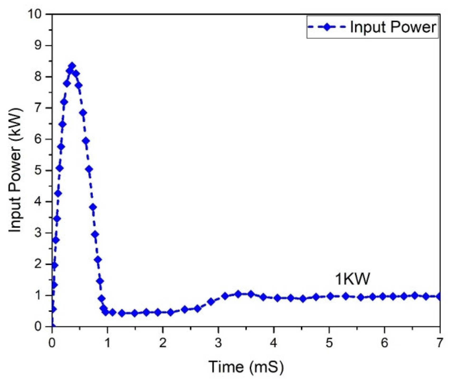
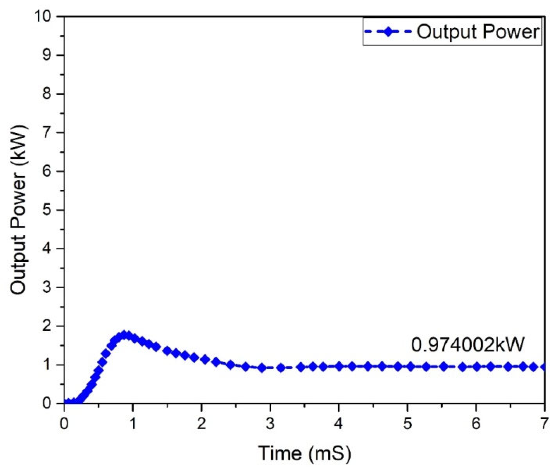
| Input power | 1 kW |
| Input voltage | 48 V |
| Input current | 20.83 Amp |
| Output voltage | 380 volts (for full bridge inverter) |
| Output current | 2.63 Amp |
| Resistance | 144.487 Ohm |
| S.NO | Parameter | Flyback-Based Converter (Si-MOSFET) (%) | Boost Converter (Si-MOSFET) | Interleaved Boost Converter (Si-MOSFET) | Flyback Boost Converter (GaN-HEMT) |
|---|---|---|---|---|---|
| 1 | Efficiency | 95 | 93.5 | 91 | 97 |
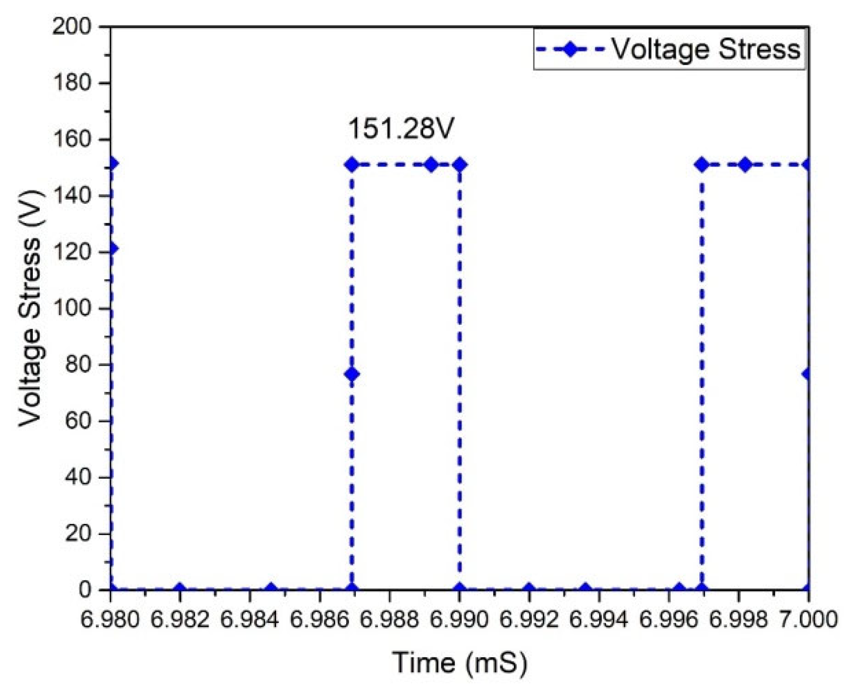
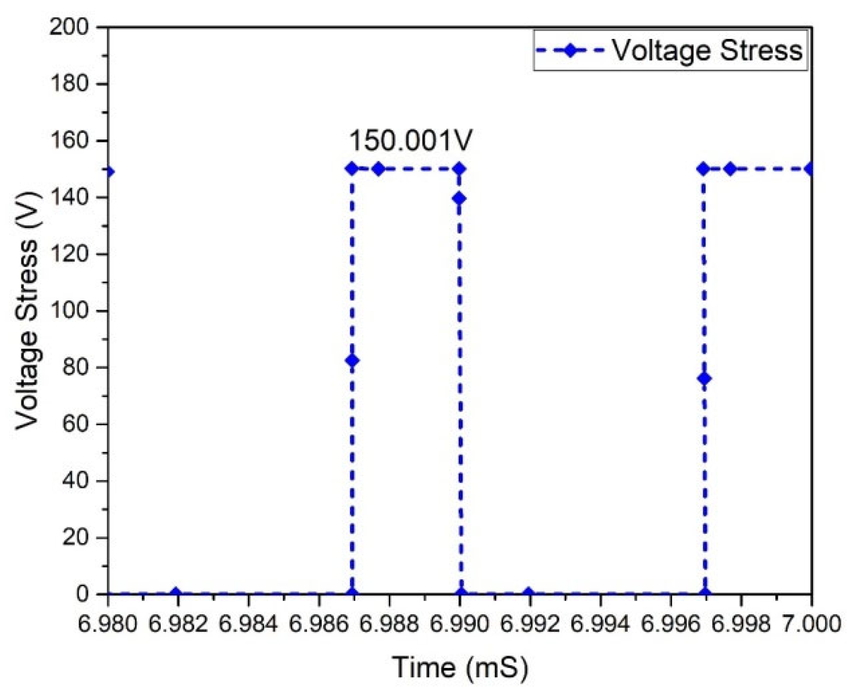
| 2 | Voltage Stress | 151.28 | 364.68 | 362.98 | 150.001 |
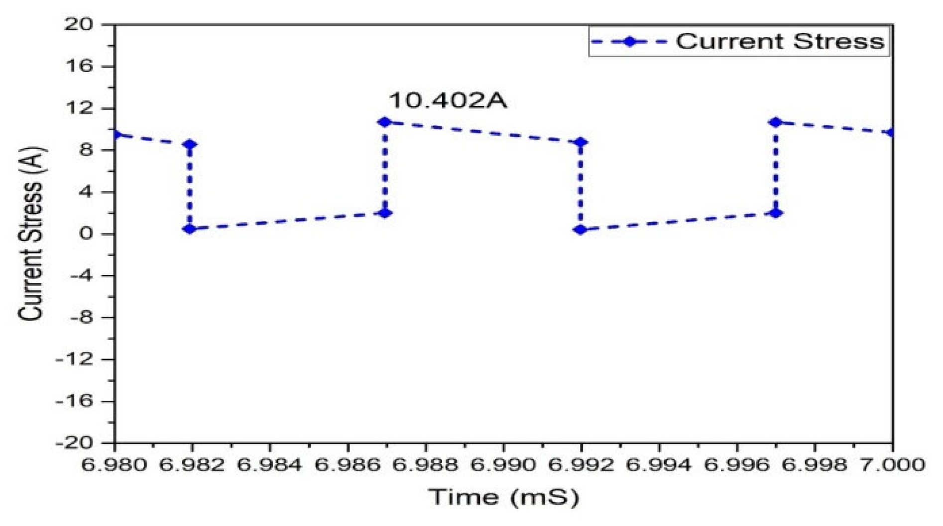
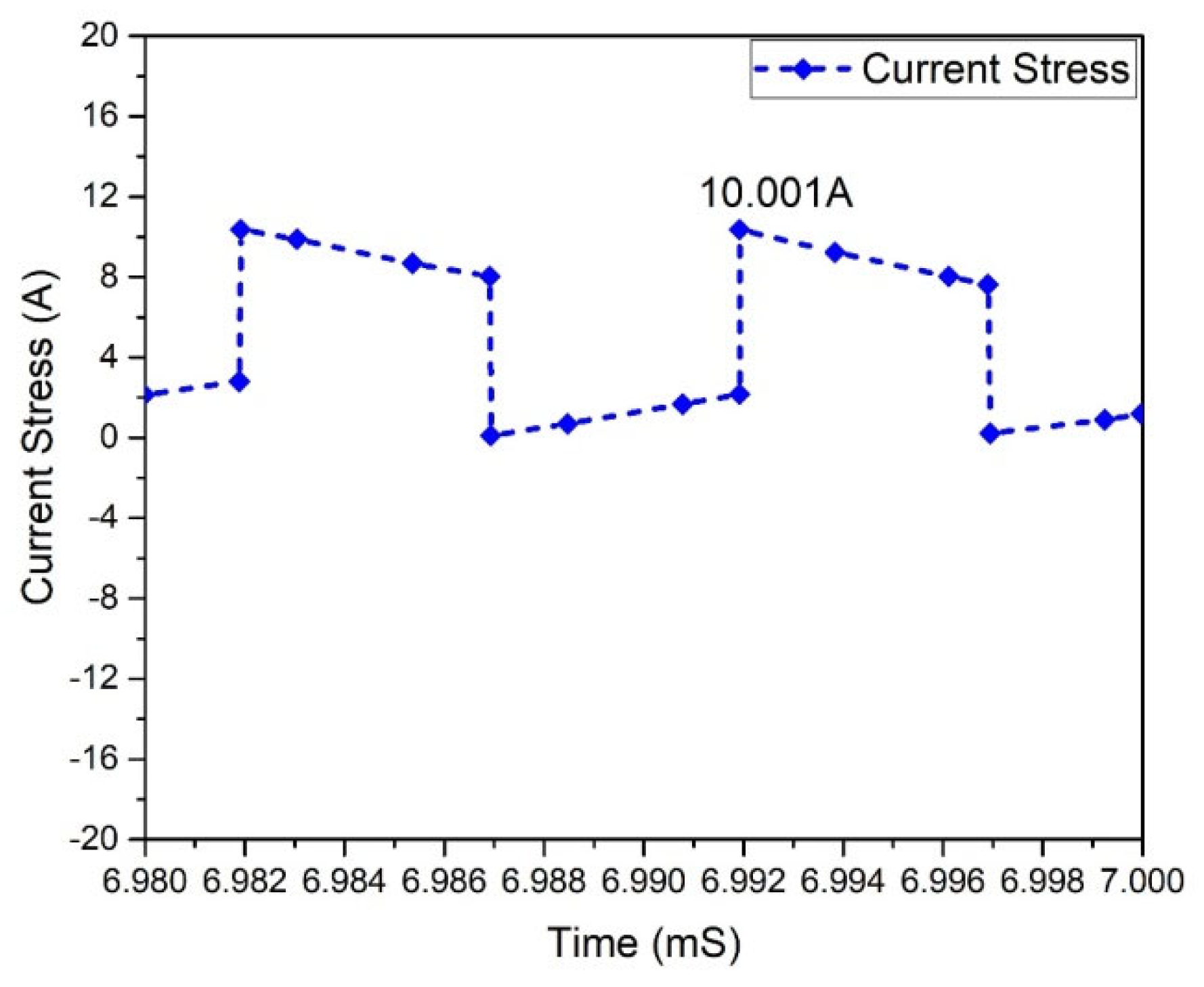
| 3 | Current Stress | 10.402 | 26.02 | 7.6327 | 10.001 |
Publisher’s Note: MDPI stays neutral with regard to jurisdictional claims in published maps and institutional affiliations. |
© 2022 by the authors. Licensee MDPI, Basel, Switzerland. This article is an open access article distributed under the terms and conditions of the Creative Commons Attribution (CC BY) license (https://creativecommons.org/licenses/by/4.0/).
Share and Cite
Salim, K.; Asif, M.; Ali, F.; Armghan, A.; Ullah, N.; Mohammad, A.-S.; Al Ahmadi, A.A. Low-Stress and Optimum Design of Boost Converter for Renewable Energy Systems. Micromachines 2022, 13, 1085. https://doi.org/10.3390/mi13071085
Salim K, Asif M, Ali F, Armghan A, Ullah N, Mohammad A-S, Al Ahmadi AA. Low-Stress and Optimum Design of Boost Converter for Renewable Energy Systems. Micromachines. 2022; 13(7):1085. https://doi.org/10.3390/mi13071085
Chicago/Turabian StyleSalim, Kashmala, Muhammad Asif, Farman Ali, Ammar Armghan, Nasim Ullah, Al-Sharef Mohammad, and Ahmad Aziz Al Ahmadi. 2022. "Low-Stress and Optimum Design of Boost Converter for Renewable Energy Systems" Micromachines 13, no. 7: 1085. https://doi.org/10.3390/mi13071085