
Virtual Stencil for Patterning and Modeling in a Quantitative Volume Using EWOD and DEP Devices for Microfluidics


Abstract
:
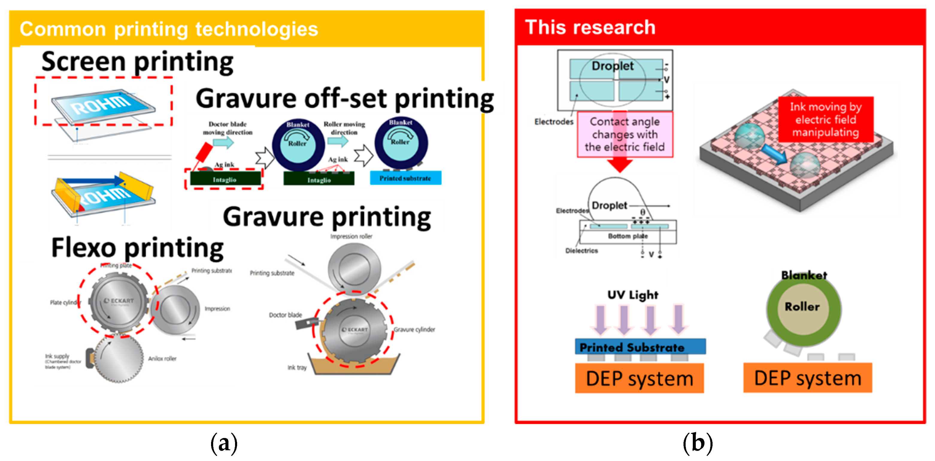
1. Introduction
2. Theoretical of Electro-Wetting Effect, Experimental Design and Setup
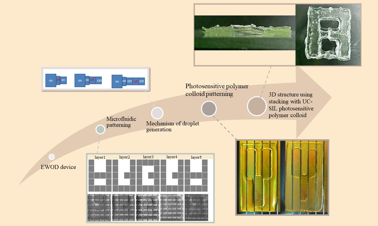
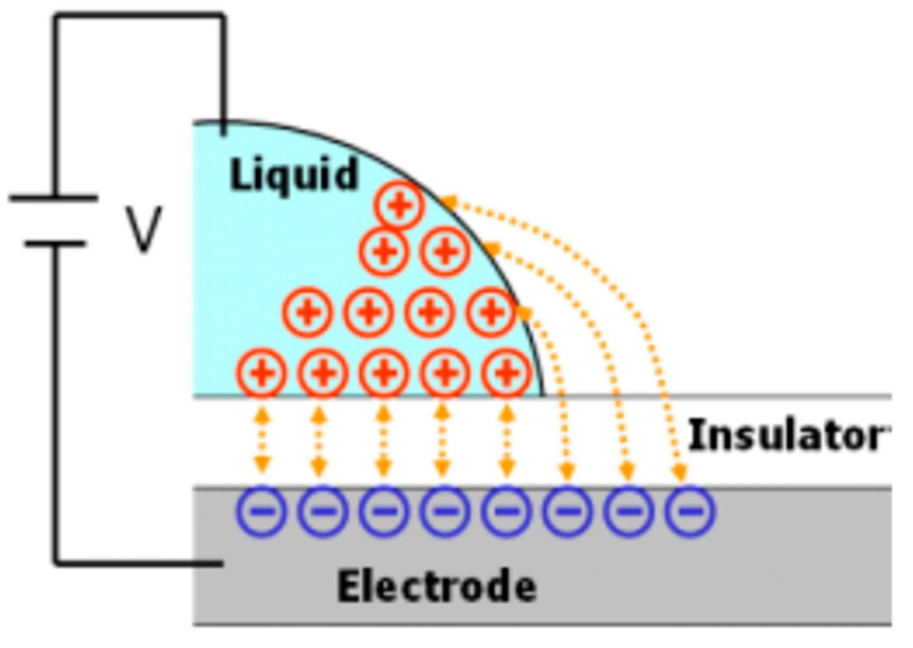
2.1. Theoretical
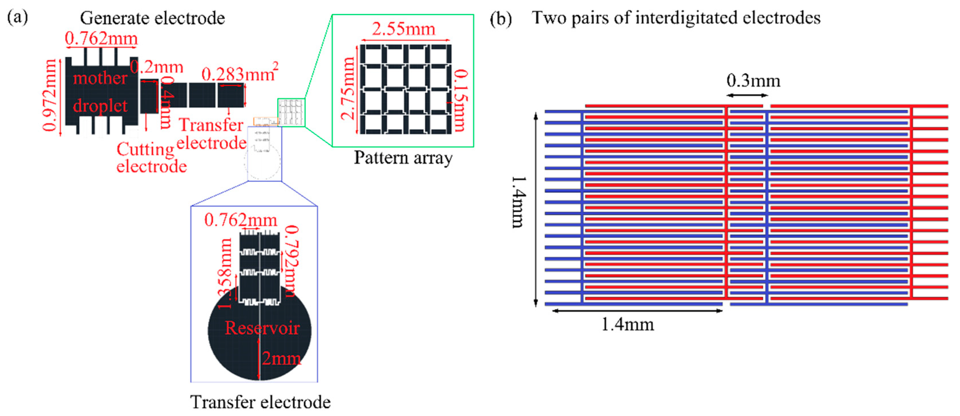
2.2. Electrode Design of EWOD Chip and DEP Chip
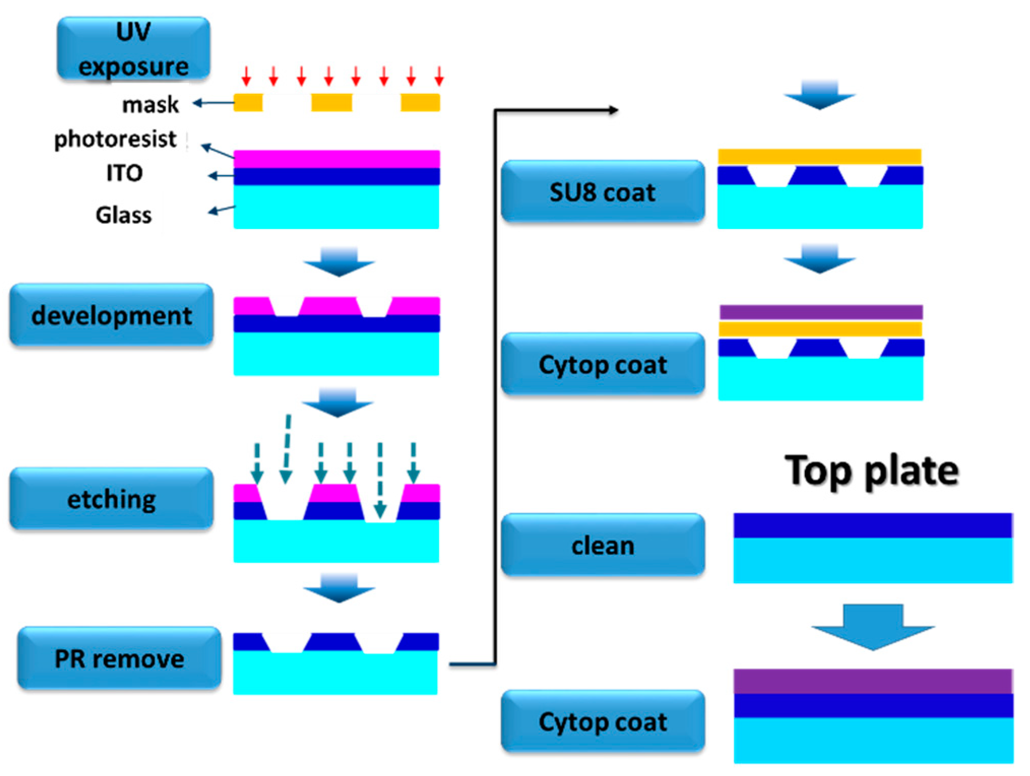
2.3. Fabrication Process of EWOD and DEP Chip
2.4. Experimental Setup
2.5. Preparation of Driving Liquid
3. Results
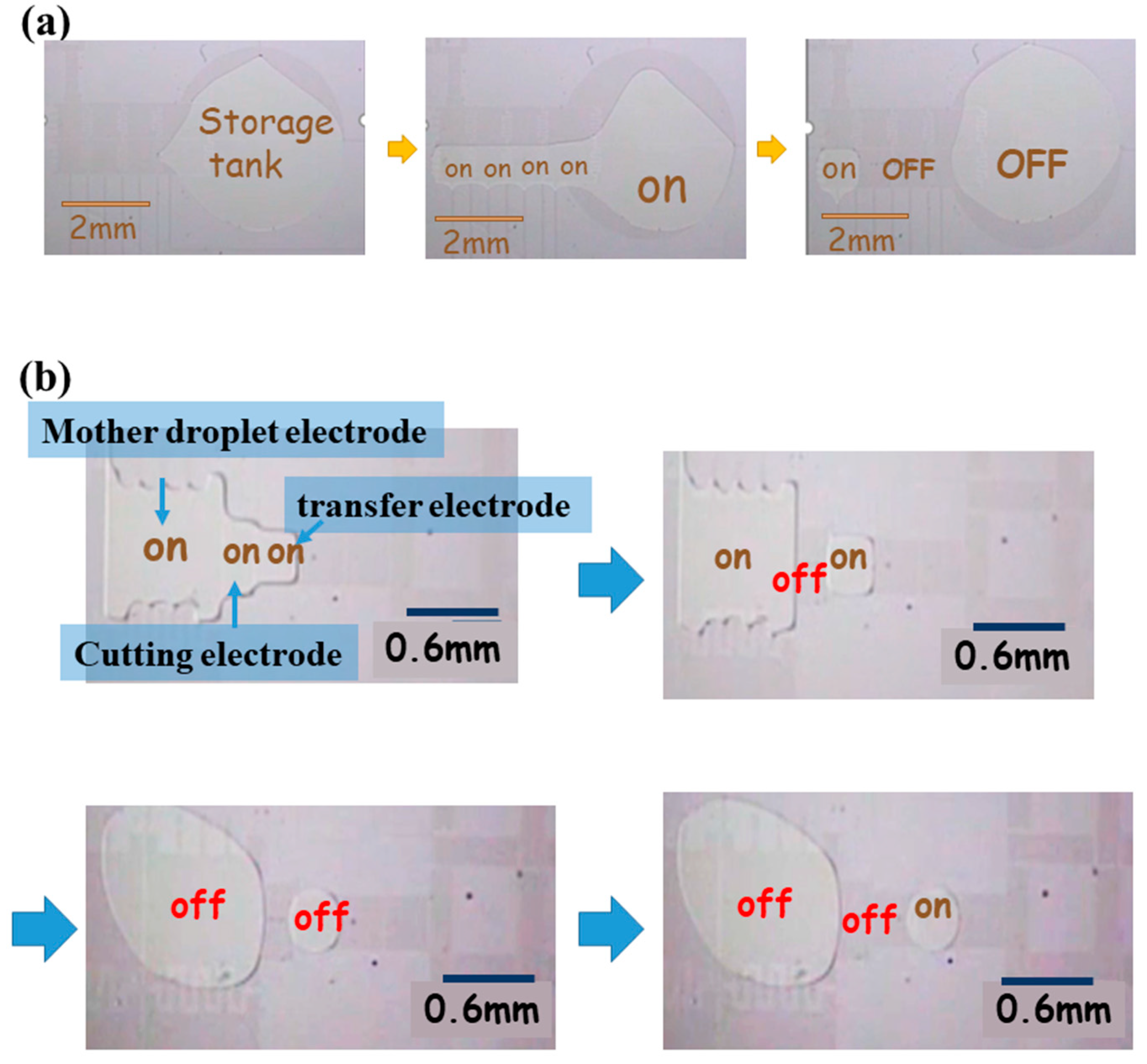
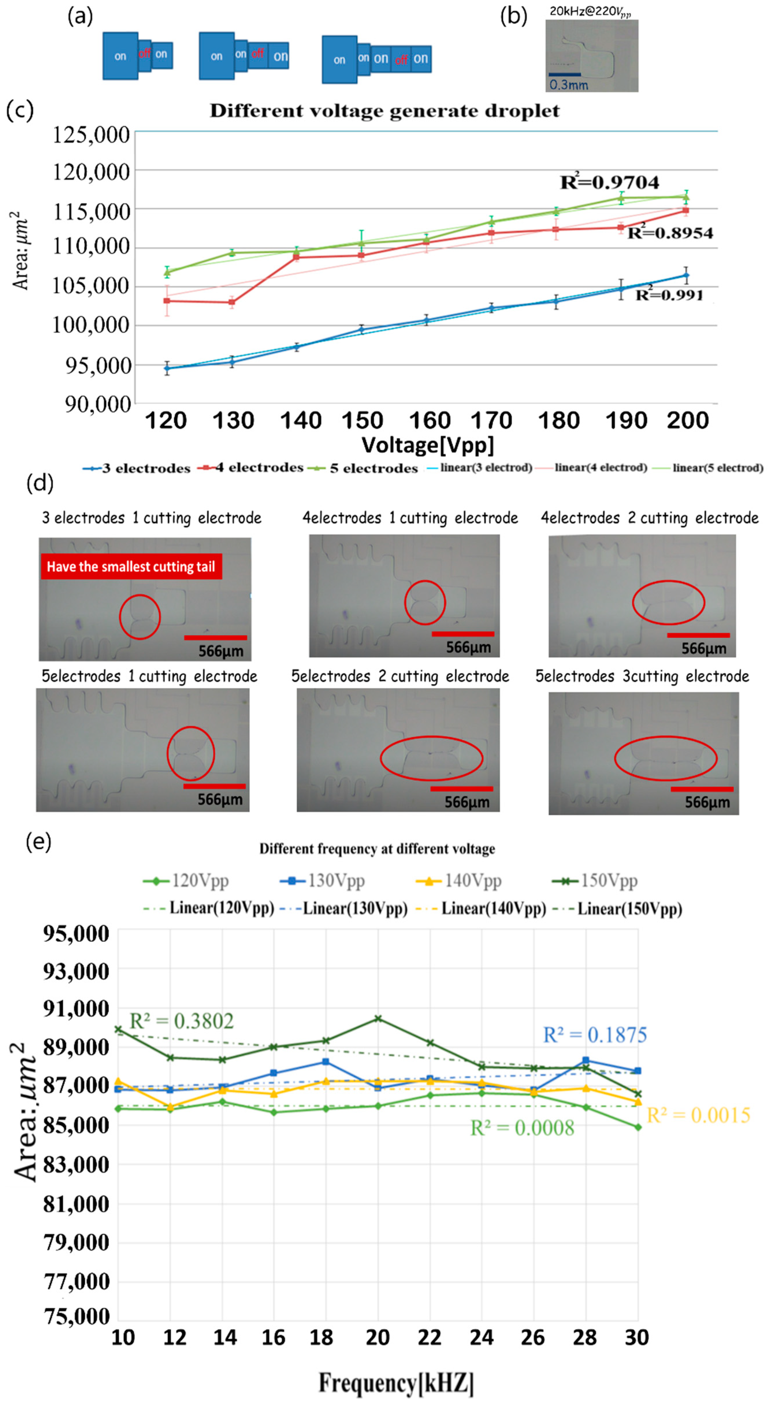
3.1. Droplet Generation
3.2. Droplet Generation in a Two-Plate Chip
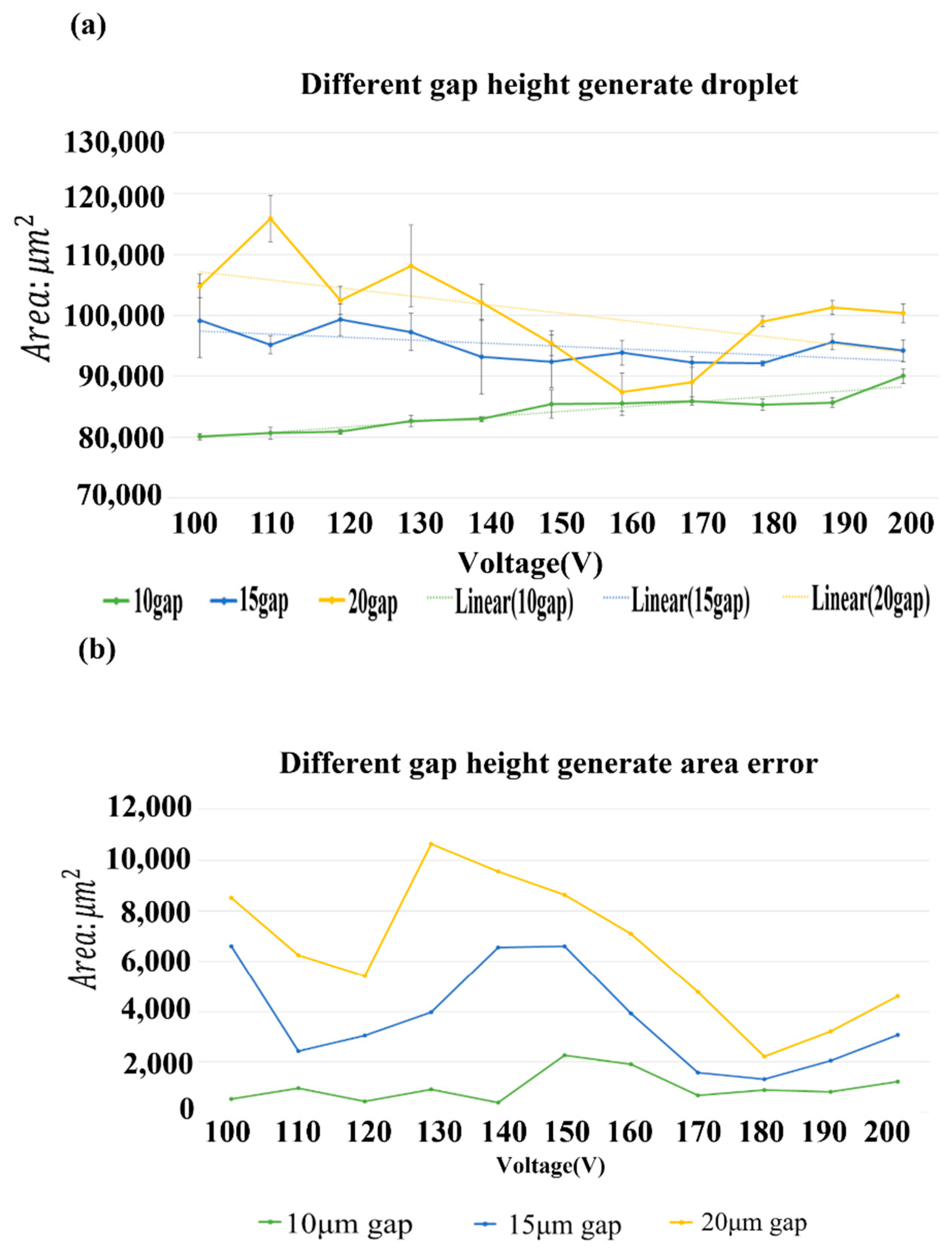
3.3. Variation of Droplet Size with Gap Height and Voltage
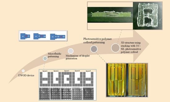
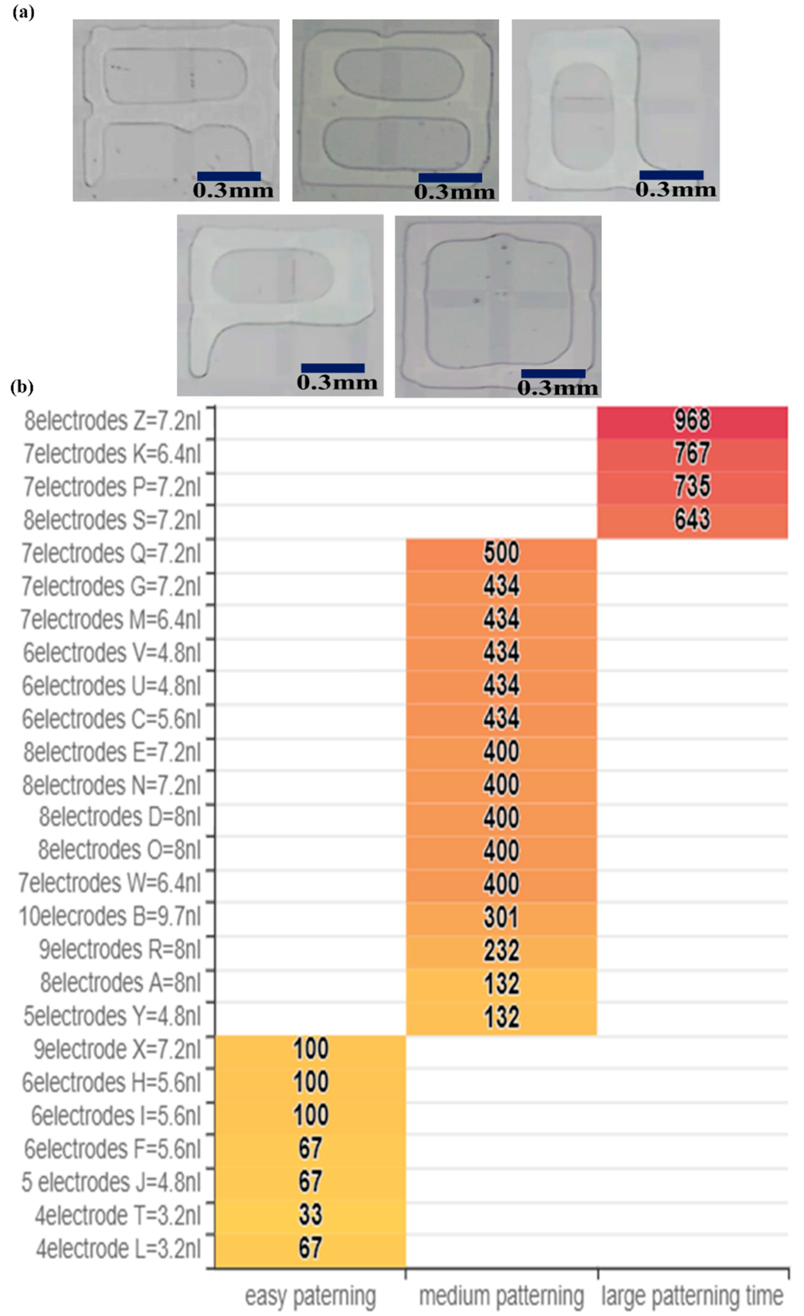
3.4. Microfluidic Patterning of 4 × 4 Array EWOD Electrodes
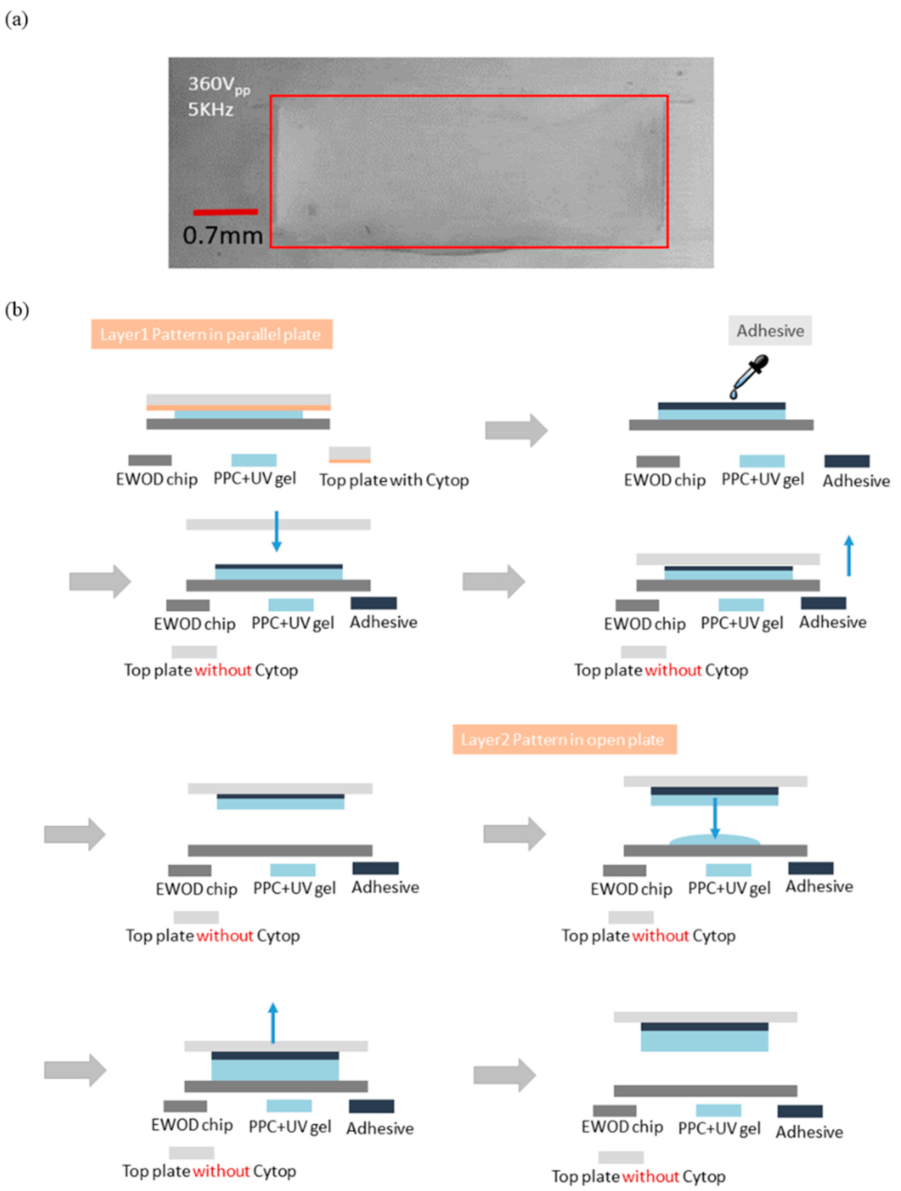
3.5. UV-SIL Photosensitive Polymer Colloid Patterning Experiment by EWOD Electrodes
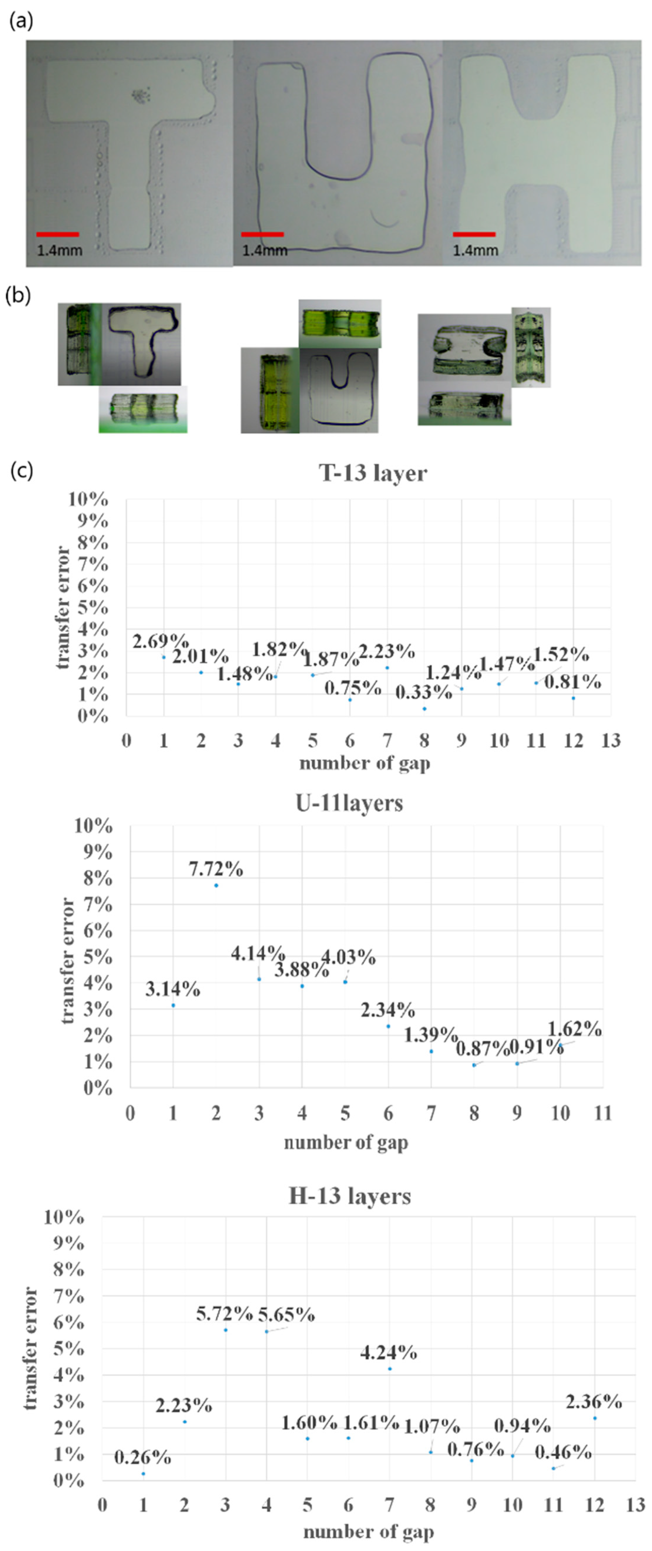
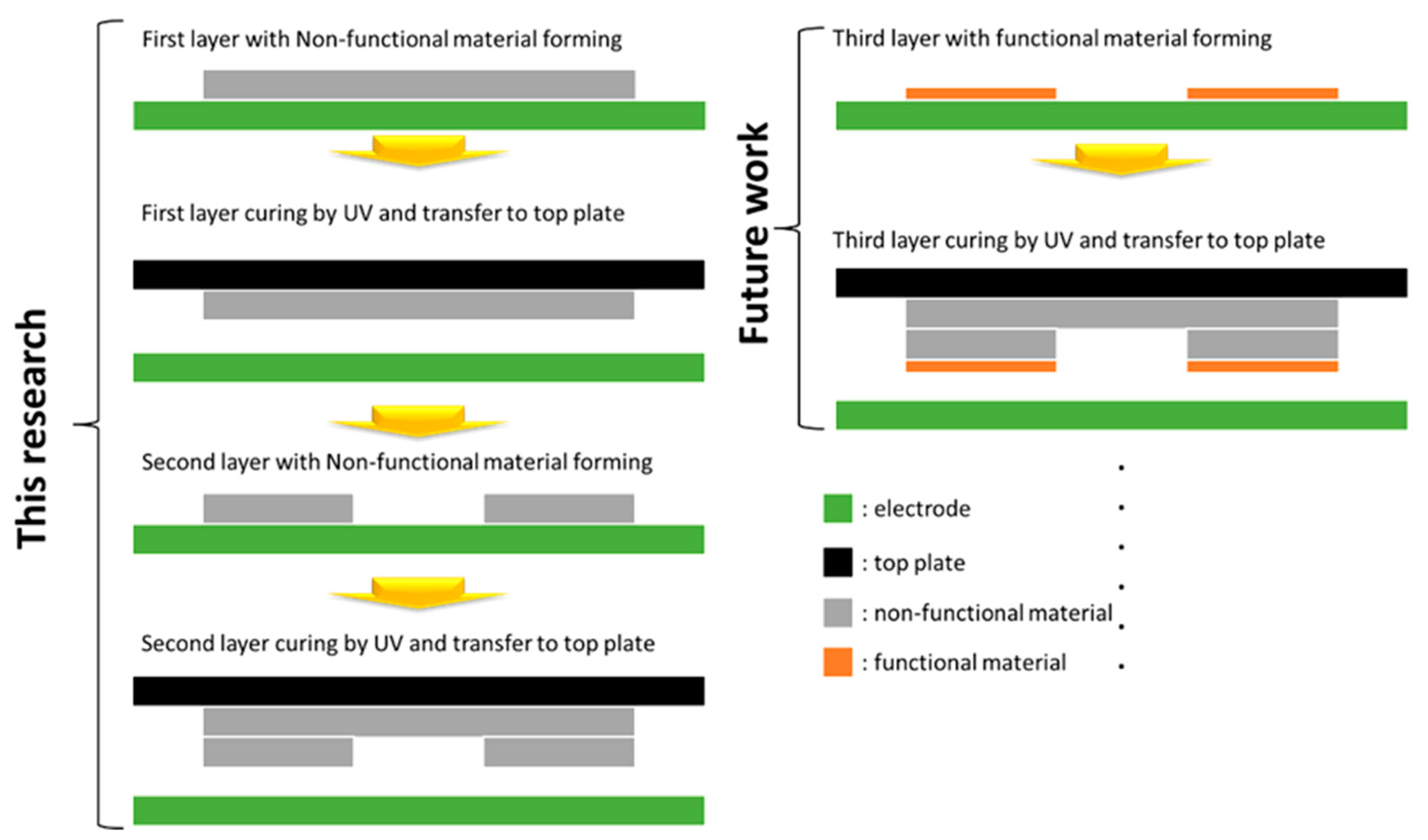
3.6. Forming a 3D Structure Using Stacking with UC-SIL Photosensitive Polymer Colloid by DEP Electrodes
4. Conclusions
Author Contributions
Funding
Conflicts of Interest
References
- Singh, M.; Haverinen, H.M.; Dhagat, P.; Jabbour, G.E. Inkjet Printing-Process and Its Applications. Adv. Mater. 2010, 22, 673–685. [Google Scholar] [CrossRef]
- Teichler, A.; Perelaer, J.; Schubert, U.S. Inkjet printing of organic electronics—Comparison of deposition techniques and state-of-the-art developments. J. Mater. Chem. C 2013, 1, 1910–1925. [Google Scholar] [CrossRef]
- Chaug, Y.; Haubrich, J.E.; Sereda, M.; Liang, R. Roll-to-Roll Processes for the Manufacturing of Patterned Conductive Electrodes on Flexible Substrates. MRS Online Proc. Libr. (OPL) 2004, 814. [Google Scholar] [CrossRef]
- Søndergaard, R.R.; Hösel, M.; Krebs, F.C. Roll-to-Roll fabrication of large area functional organic materials. J. Polym. Sci. Part B Polym. Phys. 2012, 51, 16–34. [Google Scholar] [CrossRef]
- Noh, J.; Yeom, D.; Lim, C.; Cha, H.; Han, J.; Kim, J.; Park, Y.; Subramanian, V.; Cho, G. Scalability of Roll-to-Roll Gravure-Printed Electrodes on Plastic Foils. IEEE Trans. Electron. Packag. Manuf. 2010, 33, 275–283. [Google Scholar] [CrossRef]
- Harrop, P.; Das, R. Structural Electronics 2018–2028: Applications, Technologies, Forecasts. In-Mold Electronics, Smart Skin, Structural Health Monitoring, Composite Smart Structures, Building Integrated Photovoltaics (BIPV). 2018. Available online: https://www.idtechex.com/tw/research-report/structural-electronics-2018-2028-applications-technologies-forecasts/602 (accessed on 23 July 2021).
- Huang, T.Q.; Qu, X.; Liu, J.; Chen, S. 3D printing of biomimetic microstructures for cancer cell migration. Biomed. Microdevices 2014, 16, 127–132. [Google Scholar] [CrossRef] [PubMed]
- MacDonald, E.; Salas, R.; Espalin, D.; Perez, M.; Aguilera, E.; Muse, D.; Wicker, R.B. 3D Printing for the Rapid Prototyping of Structural Electronics. IEEE Access 2014, 2, 234–242. [Google Scholar] [CrossRef]
- Au, S.H.; Shih, S.C.C.; Wheeler, A.R. Integrated microbioreactor for culture and analysis of bacteria, algae and yeast. Biomed. Microdevices 2010, 13, 41–50. [Google Scholar] [CrossRef]
- Chiang, C.-E.; Huang, H.-Y.; Lin, K.-T.; Alias, A.B.; Lu, P.-J.; Wang, Y.-W.; Wu, T.-H.; Jiang, P.-S.; Chen, C.-A.; Yao, D.-J. A medical innovation: A new and improved method of DNA extraction with electrowetting-on-dielectric of genetic testing in-vitro fertilization (IVF). Microfluid. Nanofluid. 2020, 24, 1–9. [Google Scholar] [CrossRef]
- Huang, H.-Y.; Shen, H.-H.; Chung, L.-Y.; Chung, Y.-H.; Chen, C.-C.; Hsu, C.-H.; Fan, S.-K.; Yao, D.-J. Fertilization of Mouse Gametes In Vitro Using a Digital Microfluidic System. IEEE Trans. NanoBiosci. 2015, 14, 857–863. [Google Scholar] [CrossRef]
- Jain, V.; Muralidhar, K. Electrowetting-on-Dielectric System for COVID-19 Testing. Trans. Indian Natl. Acad. Eng. 2020, 5, 251–254. [Google Scholar] [CrossRef]
- Ng, A.; Choi, K.; Luoma, R.P.; Robinson, J.M.; Wheeler, A. Digital Microfluidic Magnetic Separation for Particle-Based Immunoassays. Anal. Chem. 2012, 84, 8805–8812. [Google Scholar] [CrossRef]
- Shen, H.-H.; Chung, L.-Y.; Yao, D.-J. Improving the dielectric properties of an electrowetting-on-dielectric microfluidic device with a low-pressure chemical vapor deposited Si3N4 dielectric layer. Biomicrofluidics 2015, 9, 022403. [Google Scholar] [CrossRef] [PubMed] [Green Version]
- Cho, S.K.; Moon, H.; Fowler, J.; Fan, S.; Kim, C.-J. Splitting a liquid droplet for electrowetting-based microfluidics. In Proceedings of the 2001 ASME Inter Mech Eng Congress and Expo, New York, NY, USA, 11–16 November 2001. [Google Scholar]
- Lienemann, J.; Greiner, A.; Korvink, J.G. EDEW Version 1.0, A Simulation Tool for Fluid Handling by Electrowetting Effects; IMTEK, Albert Ludwig Univ: Freiburg, Germany, 2004. [Google Scholar]
- Song, J.H.; Evans, R.; Lin, Y.-Y.; Hsu, B.-N.; Fair, R.B. A scaling model for electrowetting-on-dielectric microfluidic actuators. Microfluid. Nanofluid. 2009, 7, 75–89. [Google Scholar] [CrossRef]
- Gong, J.; Kim, C.-J. “cj” All-electronic droplet generation on-chip with real-time feedback control for EWOD digital microfluidics. Lab Chip 2008, 8, 898–906. [Google Scholar] [CrossRef] [PubMed]
- Samiei, E.; Tabrizian, M.; Hoorfar, M. A review of digital microfluidics as portable platforms for lab-on a-chip applications. Lab Chip 2016, 16, 2376–2396. [Google Scholar] [CrossRef]
- Reyes, D.R.; Iossifidis, D.; Auroux, P.-A.; Manz, A. Micro Total Analysis Systems. 1. Introduction, Theory, and Technology. Anal. Chem. 2002, 74, 2623–2636. [Google Scholar] [CrossRef]
- Tang, T.; Yuan, Y.; Yalikun, Y.; Hosokawa, Y.; Li, M.; Tanaka, Y. Glass based micro total analysis systems: Materials, fabrication methods, and applications. Sens. Actuators B Chem. 2021, 339, 129859. [Google Scholar] [CrossRef]
- Auroux, P.-A.; Iossifidis, D.; Reyes, D.R.; Manz, A. Micro Total Analysis Systems. 2. Analytical Standard Operations and Applications. Anal. Chem. 2002, 74, 2637–2652. [Google Scholar] [CrossRef]
- Pandey, C.M.; Augustine, S.; Kumar, S.; Kumar, S.; Nara, S.; Srivastava, S.; Malhotra, B.D. Microfluidics Based Point-of-Care Diagnostics. Biotechnol. J. 2018, 13, 1700047. [Google Scholar] [CrossRef]
- Wang, D.-S.; Fan, S.-K. Microfluidic Surface Plasmon Resonance Sensors: From Principles to Point-of-Care Applications. Sensors 2016, 16, 1175. [Google Scholar] [CrossRef] [PubMed] [Green Version]
- Chiu, C.-P.; Chen, W.-J.; Fan, S.-K. Enhanced Droplet Mixer by LDEP on Spiral Microelectrodes. In Proceedings of the 2007 2nd IEEE International Conference on Nano/Micro Engineered and Molecular Systems, Bangkok, Thailand, 16–19 January 2007; pp. 951–954. [Google Scholar]
- Lin, Y.-C.; Chuang, K.-C.; Wang, T.-T.; Chiu, C.-P.; Fan, S.-K. Integrated Digital and Analog Microfluidics by EWOD and LDEP. In Proceedings of the 2006 1st IEEE International Conference on Nano/Micro Engineered and Molecular Systems, Zhuhai, China, 18–21 January 2006; pp. 1414–1417. [Google Scholar]
- Renaudot, R.; Agache, V.; Fouillet, Y.; Laffite, G.; Bisceglia, E.; Jalabert, L.; Kumemura, M.; Collard, D.; Fujita, H. A programmable and reconfigurable microfluidic chip. Lab. Chip 2013, 13, 4517. [Google Scholar] [CrossRef] [PubMed]
- Ciou, Y.-J.; Lee, H.-T.; Lin, Y.-W.; Yao, D.-J. Microfluidic patterning using a digital microfluidic system. AIP Adv. 2020, 10, 125115. [Google Scholar] [CrossRef]
- Alias, A.B.; Chiang, C.-E.; Huang, H.-Y.; Lin, K.-T.; Lu, P.-J.; Wang, Y.-W.; Wu, T.-H.; Jiang, P.-S.; Chen, C.-A.; Yao, D.-J. Extraction of Cell-free Dna from An Embryo-culture Medium Using Micro-scale Bio-reagents on Ewod. Sci. Rep. 2020, 10, 9708. [Google Scholar] [CrossRef] [PubMed]
- Lee, M.-S.; Hsu, W.; Huang, H.-Y.; Tseng, H.-Y.; Lee, C.-T.; Hsu, C.-Y.; Shieh, Y.-C.; Wang, S.-H.; Yao, D.-J.; Liu, C.-H. Simultaneous detection of two growth factors from human single-embryo culture medium by a bead-based digital microfluidic chip. Biosens. Bioelectron. 2020, 150, 111851. [Google Scholar] [CrossRef]
- Mugele, F.; Baret, J.-C. Electrowetting: From basics to applications. J. Phys. Condens. Matter 2005, 17, R705–R774. [Google Scholar] [CrossRef]
- Zhao, Y.-P.; Wang, Y. Fundamentals and Applications of Electrowetting. Rev. Adhes. Adhes. 2013, 1, 114–174. [Google Scholar] [CrossRef]
- Li, J.; Kim, C.-J. “Cj” Current commercialization status of electrowetting-on-dielectric (EWOD) digital microfluidics. Lab Chip 2020, 20, 1705–1712. [Google Scholar] [CrossRef]
- Teng, P.; Tian, D.; Fu, H.; Wang, S. Recent progress of electrowetting for droplet manipulation: From wetting to superwetting systems. Mater. Chem. Front. 2019, 4, 140–154. [Google Scholar] [CrossRef]
- Banerjee, A.; Noh, J.H.; Liu, Y.; Rack, P.D.; Papautsky, I. Programmable Electrowetting with Channels and Droplets. Micromachines 2015, 6, 172–185. [Google Scholar] [CrossRef]
- Li, H.-T.; Huang, Y.-H.; Yao, D.-J. Using EWOD Chip for the Culture Medium Movement and Dynamic Culture of Mouse Embryos. In Proceedings of the 2018 IEEE Micro Electro Mechanical Systems (MEMS), Belfast, UK, 21–25 January 2018; pp. 1138–1141. [Google Scholar] [CrossRef]
- Zeng, J.; Korsmeyer, T. Principles of droplet electrohydrodynamics for lab-on-a-chip. Lab Chip 2004, 4, 265–277. [Google Scholar] [CrossRef] [PubMed]
- Wheeler, A.; Moon, H.; Kim, C.-J.; Loo, J.A.; Garrell, R.L. Electrowetting-Based Microfluidics for Analysis of Peptides and Proteins by Matrix-Assisted Laser Desorption/Ionization Mass Spectrometry. Anal. Chem. 2004, 76, 4833–4838. [Google Scholar] [CrossRef] [PubMed]
- Plog, J.; LÖwe, J.-M.; Jiang, Y.; Pan, Y.; Yarin, A. Control of direct written ink droplets using electrowetting. Langmuir 2019, 35, 11023–11036. [Google Scholar] [CrossRef] [PubMed]
- Liu, Y.; Banerjee, A.; Papautsky, I. Precise droplet volume measurement and electrode-based volume metering in digital microfluidics. Microfluid. Nanofluid. 2014, 17, 295–303. [Google Scholar] [CrossRef]
- Lippmann, G. Relations Entre les Phénomènes Électriques et Capillaires; Gauthier-Villars: Paris, France, 1875. [Google Scholar]
- Berge, B. Electrocapillarite et mouillage de films isolants par l’eau. Comptes rendus de l’Académie des sciences. Série 2 Mécanique Phys. Chim. Sci. De L’univers Sci. De La Terre 1993, 317, 157–163. [Google Scholar]
- Lee, J.; Kim, C.-J. “cj” Surface-tension-driven microactuation based on continuous electrowetting. J. Microelectromech. Syst. 2000, 9, 171–180. [Google Scholar] [CrossRef]
- Vallet, M.; Berge, B.; Vovelle, L. Electrowetting of water and aqueous solutions on poly(ethylene terephthalate) insulating films. Polymer 1996, 37, 2465–2470. [Google Scholar] [CrossRef]
- Jones, T.B. On the Relationship of Dielectrophoresis and Electrowetting. Langmuir 2002, 18, 4437–4443. [Google Scholar] [CrossRef]
- Moon, H.; Cho, S.K.; Garrell, R.L.; Kim, C.-J. “cj” Low voltage electrowetting-on-dielectric. J. Appl. Phys. 2002, 92, 4080–4087. [Google Scholar] [CrossRef]
- Cho, S.K.; Moon, H.; Kim, C.-J. Creating, transporting, cutting, and merging liquid droplets by electrowetting-based actuation for digital microfluidic circuits. J. Microelectromech. Syst. 2003, 12, 70–80. [Google Scholar] [CrossRef] [Green Version]
- Shapiro, B.; Moon, H.; Garrell, R.L.; Kim, C.-J. Equilibrium behavior of sessile drops under surface tension, applied external fields, and material variations. J. Appl. Phys. 2003, 93, 5794–5811. [Google Scholar] [CrossRef] [Green Version]
- Baird, E.; Young, P.; Mohseni, K. Electrostatic force calculation for an EWOD-actuated droplet. Microfluid. Nanofluid. 2007, 3, 635–644. [Google Scholar] [CrossRef]
- Bonart, H.; Kahle, C.; Repke, J.-U. Optimal Control of Droplets on a Solid Surface Using Distributed Contact Angles. Langmuir 2020, 36, 8894–8903. [Google Scholar] [CrossRef] [PubMed]


| English alphabet | A | B | C | D | E | F | G |
| Electrode number | 8 | 10 | 6 | 8 | 8 | 6 | 8 |
| Droplet volume (nL) | 8.30 | 9.96 | 5.81 | 8.30 | 7.47 | 5.81 | 7.47 |
| English alphabet | H | I | J | K | L | M | N |
| Electrode number | 6 | 6 | 5 | 7 | 4 | 7 | 8 |
| Droplet volume (nL) | 5.81 | 5.81 | 4.98 | 5.81 | 3.32 | 6.64 | 7.47 |
| English alphabet | O | P | Q | R | S | T | U |
| Electrode number | 8 | 7 | 7 | 9 | 8 | 4 | 6 |
| Droplet volume (nL) | 8.30 | 7.47 | 7.47 | 8.30 | 7.47 | 3.32 | 4.98 |
| English alphabet | V | W | X | Y | Z | ||
| Electrode number | 6 | 7 | 8 | 5 | 8 | ||
| Droplet volume (nL) | 4.98 | 6.64 | 7.47 | 4.98 | 7.47 |
| English alphabet. | A | B | C | D | E | F | G |
| Electrode number | 8 | 10 | 6 | 8 | 8 | 6 | 8 |
| volume (nL) | 8.08 | 9.70 | 5.66 | 8.08 | 7.27 | 5.66 | 7.27 |
| English alphabet | H | I | J | K | L | M | N |
| Electrode number | 6 | 6 | 5 | 7 | 4 | 7 | 8 |
| volume (nL) | 5.66 | 5.66 | 4.85 | 6.46 | 3.23 | 6.46 | 7.27 |
| English alphabet | O | P | Q | R | S | T | U |
| Electrode number | 8 | 7 | 7 | 9 | 8 | 4 | 6 |
| volume (nL) | 8.08 | 7.27 | 7.27 | 8.08 | 7.27 | 3.23 | 4.85 |
| English alphabet | V | W | X | Y | Z | ||
| Electrode number | 6 | 7 | 8 | 5 | 8 | ||
| volume (nL) | 4.85 | 6.46 | 7.27 | 4.85 | 7.27 |
Publisher’s Note: MDPI stays neutral with regard to jurisdictional claims in published maps and institutional affiliations. |
© 2021 by the authors. Licensee MDPI, Basel, Switzerland. This article is an open access article distributed under the terms and conditions of the Creative Commons Attribution (CC BY) license (https://creativecommons.org/licenses/by/4.0/).
Share and Cite
Lin, Y.-W.; Ciou, Y.-J.; Yao, D.-J. Virtual Stencil for Patterning and Modeling in a Quantitative Volume Using EWOD and DEP Devices for Microfluidics. Micromachines 2021, 12, 1104. https://doi.org/10.3390/mi12091104
Lin Y-W, Ciou Y-J, Yao D-J. Virtual Stencil for Patterning and Modeling in a Quantitative Volume Using EWOD and DEP Devices for Microfluidics. Micromachines. 2021; 12(9):1104. https://doi.org/10.3390/mi12091104
Chicago/Turabian StyleLin, Yi-Wei, Ying-Jhen Ciou, and Da-Jeng Yao. 2021. "Virtual Stencil for Patterning and Modeling in a Quantitative Volume Using EWOD and DEP Devices for Microfluidics" Micromachines 12, no. 9: 1104. https://doi.org/10.3390/mi12091104