Article

Rapid Fabrication of Large-Area Concave Microlens Array on ZnSe

1
State Key Laboratory for Manufacturing System Engineering, School of Electronic Science and Engineering, Xi’an Jiaotong University, Xi’an 710049, China
2
School of Mechanical Engineering, Xi’an Jiaotong University, Xi’an 710049, China
*
Authors to whom correspondence should be addressed.
Micromachines 2021, 12(4), 458; https://doi.org/10.3390/mi12040458
Submission received: 8 March 2021 / Revised: 30 March 2021 / Accepted: 12 April 2021 / Published: 19 April 2021

Abstract

:
A rapid and single-step method for the fabrication of a zinc selenide (ZnSe) concave microlens array through the high-speed line-scanning of a femtosecond laser pulse is presented. Approximately 1.1 million microlenses, with minimized volume and high transparency at wavelengths between approximately 0.76–20 μm were fabricated within 36 min. More importantly, the size of the microlenses can be controlled by adjusting the laser power. Their high-quality infrared optical performance was also demonstrated. This method holds great promise for the development of ZnSe-based micro-optical devices.

1. Introduction

Microlens arrays (MLAs) have diverse applications for infrared detection [1], beam homogenization [2], microimaging [3], optical communication [4,5], and microfabrication [6]. At present, silicon and quartz are widely used for processing MLAs. However, the infrared cutoff wavelength of quartz is shorter (the longest wavelength is approximately 3.5 μm). In the very important atmospheric transparent second (3–5 μm) and third (8–12 μm) windows, quartz material cannot transmit light, and silicon and quartz are limited in nonlinear applications owing to their low nonlinear characteristics [7,8].
As an important II–VI semiconductor, zinc selenide (ZnSe) was one of the earliest discovered semiconductors, and is probably one of the most critical electronic and optoelectronic materials, with outstanding applications in nonlinear devices [9]. Compared with silicon and quartz, ZnSe has an excellent medium and far infrared transmittance (0.5–22 μm), a high refractive index (2.3–2.5), and a high nonlinear refractive index (8.3 × 10⁻¹⁸ m2/W) [10,11]. ZnSe has good mechanical properties, high thermal conductivity, and is insoluble in water. It cannot be ruptured under normal mechanical pressure or impact. Due to its excellent chemical and physical properties, ZnSe has been widely used in solar cells, lasers, logic gates, flat panel displays and transistors [12,13,14,15]. Recently, ZnSe has garnered tremendous interest because of its valuable potential for both basic physical research and applications in micro-nano component construction.
ZnSe is relatively easy to process as a soft crystal. At present, manufacturing techniques have been developed, including lacquer disk technology, traditional grinding and polishing, and single-point diamond turning [16,17]. Despite tremendous progress, there are still some limitations among these techniques, such as high time consumption, high process complexity, and difficulty in consistency control [18]. As an appealing alternative, femtosecond laser manufacturing has become a powerful tool for processing optical devices based on a wide range of materials, including semiconductors [19], metals [20], and dielectrics [21]. Earlier reports have already proven the effectiveness of the femtosecond laser ablation and etching technologies for fabricating optical devices [22,23,24]. However, the etching process involved in this technology still takes a lot of time.
In this work, we propose a rapid process for the realization of large-area concave infrared MLAs that addresses the limitations of traditional technologies. Our method, a rapid single-step process, exploits a high-speed femtosecond laser scanning technology. Each microlens can be formed by a femtosecond laser pulse. Within 36 min, approximately 1.1 million microlenses can be fabricated. The ablation crater of ZnSe can directly form a concave microlens under laser irradiation. The range of laser power is discussed, and we conclude how the uniformity of the structures is achieved. Furthermore, this article shows the three-dimensional (3D) morphology, as well as the IR optical properties, of the MLAs.

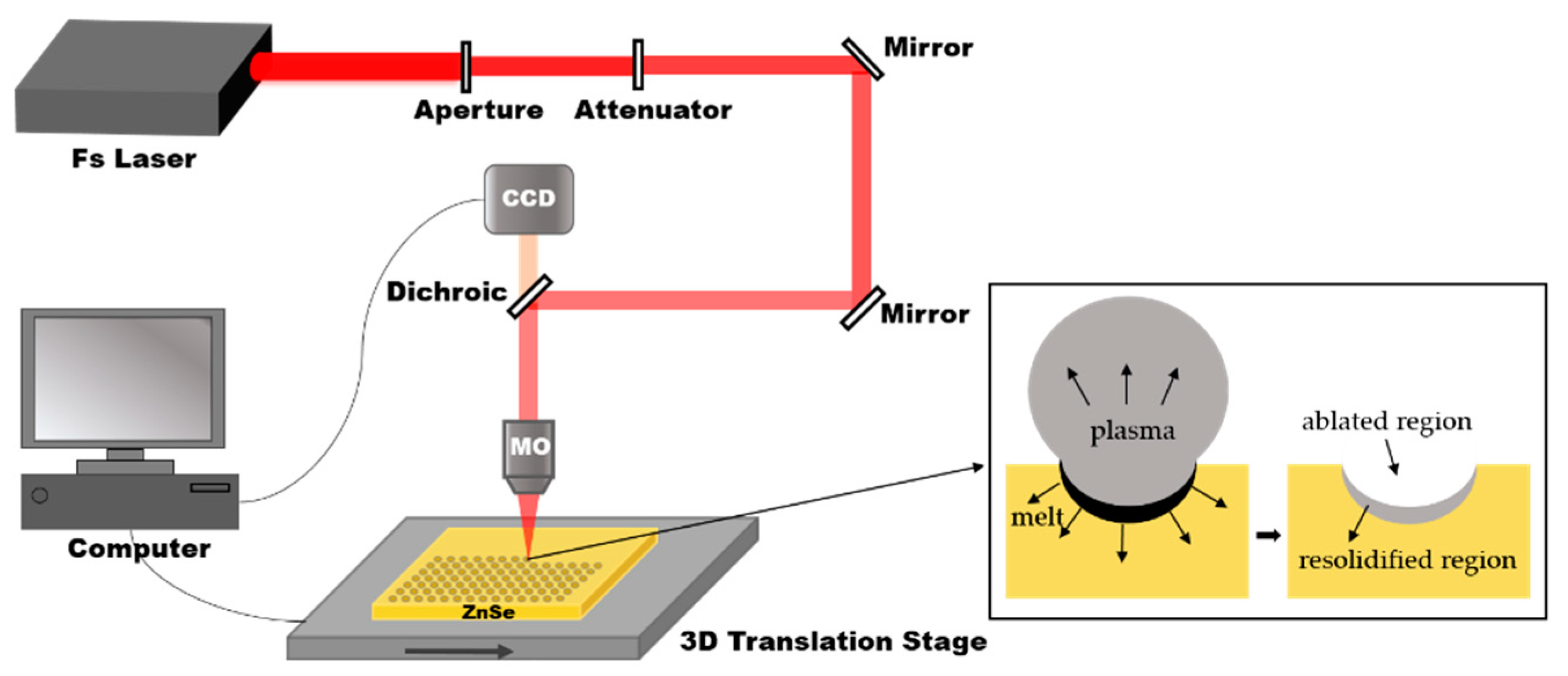
2. Materials and Methods

The IR ZnSe MLAs manufacturing process includes only one step: a fast femtosecond laser scanning process, as shown in Figure 1. In the present experiment, a commercial ZnSe sample (II–VI Incorporated, Pittsburgh, PA, USA) was used. The ZnSe was installed on the 3D translation stage (Prior Scientific, Cambridge, England, 10 ≤ v ≤ 20 mm/s ) after ultrasonic cleaning in deionized water for 10 min and drying in ambient atmosphere. The laser was generated from a regenerative, amplified Ti: sapphire laser system (Coherent Libra-usp-he; pulse duration: 50 fs; central wavelength: 800 nm; repetition rate: 1 kHz). Different optical density filters can change the pulse energy, which can be set to 5–30 mW. The laser beam was focused on the ZnSe surface through a 0.45 NA, 20X objective lens (Nikon). The femtosecond laser exposure spots were generated point-by-point by the pulsed laser system. A parabolic microlens was formed on the surface of the ZnSe due to the Gaussian distribution of the femtosecond laser beam and the unbalanced energy deposition of the laser pulses to the sample. In the fast-scanning process, the average distance between the adjacent microlenses was adjusted by the transverse scanning speed. For example, the sample was translated in a direction perpendicular to the laser beam at a speed of 12 mm/s; the microlenses, with a separation space of 12 μm, were generated at a laser repetition rate of 1 kHz per second.
Scanning electron microscopy (SEM) images of the fabricated microlenses were observed using a Flex 1000 scanning electron microscope (Hitachi, Tokyo, Japan). A LEXT-OLS4000 laser confocal microscope (Olympus, Japan) (Olympus, Tokyo, Japan) was used to obtain the three-dimensional topography and the corresponding profile curves.

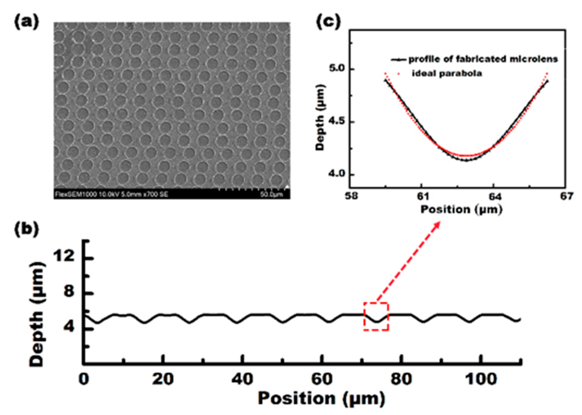
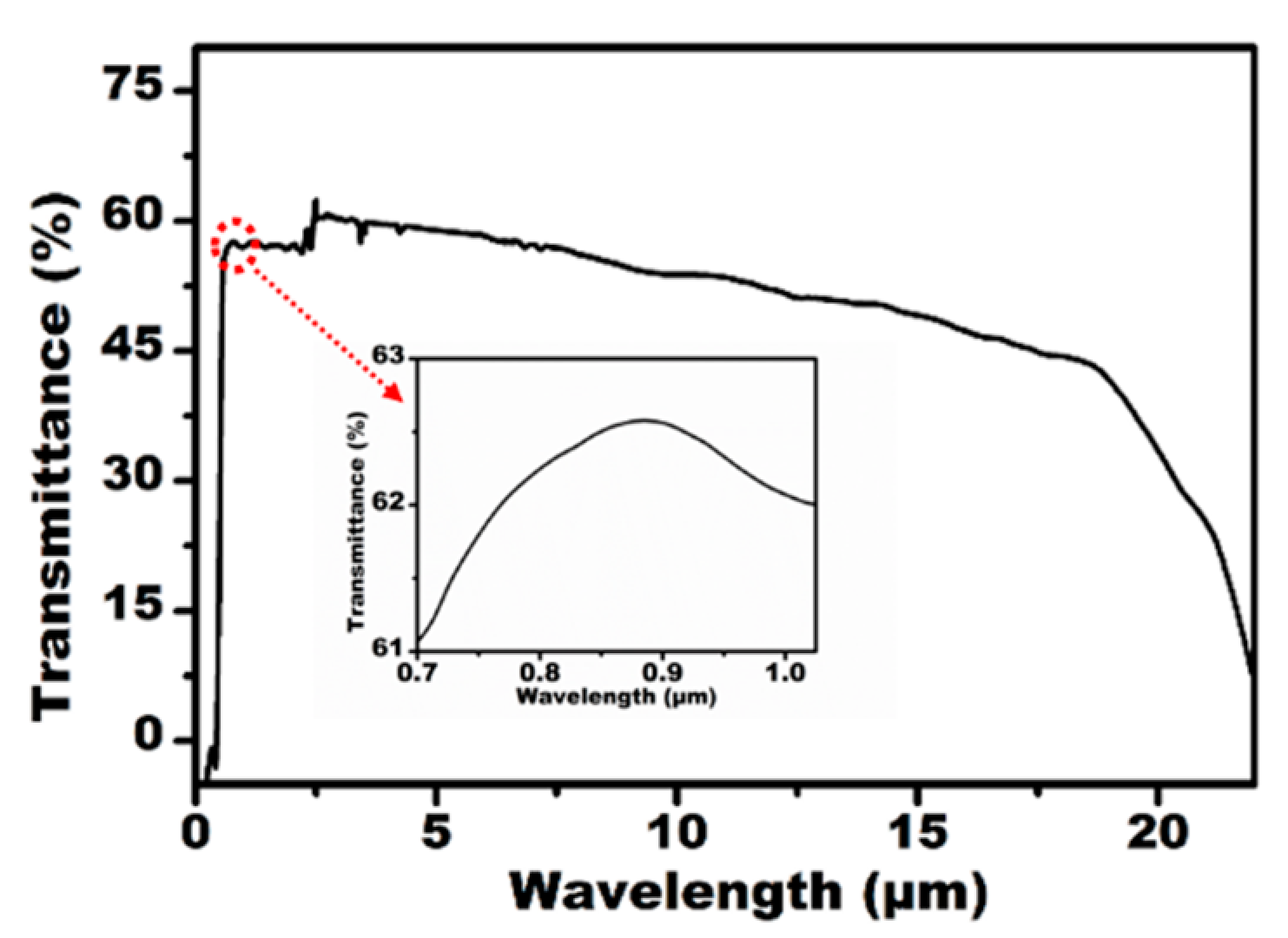
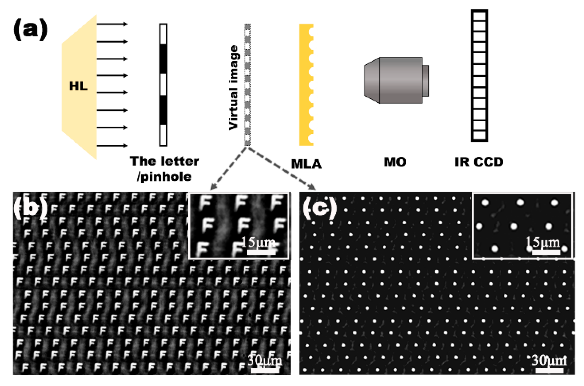
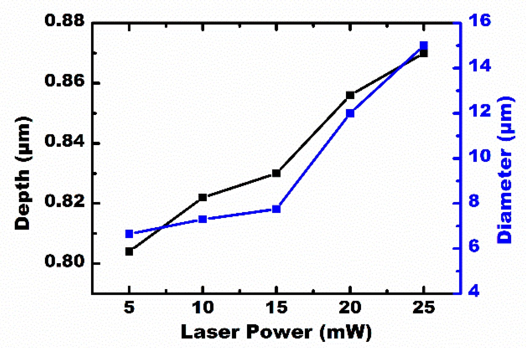
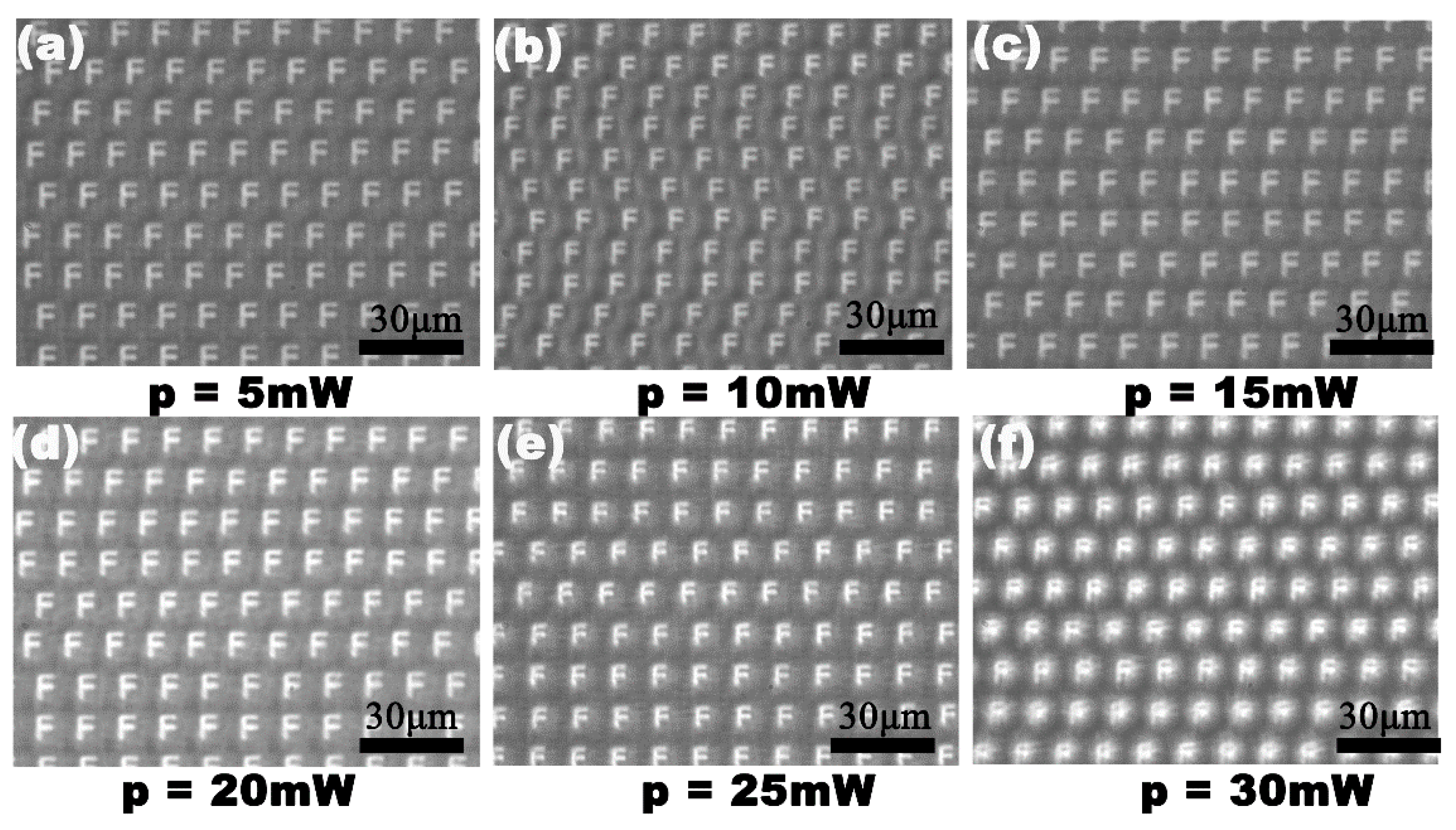
3. Results and Discussion

With the scanning speed set at 15 mm/s and the pulse energy set at 5 mW quasi-periodic microlenses, with an average size of 15 μm, could be observed, and 1000 microlenses were generated per second at a laser repetition rate of 1 kHz. The processing efficiency was 1 × 10⁵ times higher than that of the femtosecond laser direct writing method [25]. Figure 2a shows the SEM image of the MLA. Figure 2b shows the cross-sectional profile of several microlenses measured along the scanning direction. The measurement results show that the average diameter (D) of the IR microlens is 6.65 μm, and the depth (h) is 0.804 μm. Moreover, according to the measurements and the theoretical fitting data, as shown in Figure 2c, the microlenses have a parabolic shape. Furthermore, the radius of the curvature (R), the focal length (f), and the numerical aperture (NA) of the microlenses with a parabolic surface are calculated as:
R = D2/8h, f = R/(n − 1), NA = D/2f
where h is the sag height of the microlens, n = 2.63 is the refractive index of ZnSe, and D is the diameter of the microlens. Given D = 6.65 μm and h = 0.804 μm, we have R = 6.87 μm, f = 4.21 μm, and NA = 0.789.
The shape of the single-shot ablation areas shows a smooth crater surrounded by an elevated rim. The formation mechanism of a microlens is presented by analogy with Ben-Yakar’s theory. The major advantages of the femtosecond laser include its ability to produce a very high peak intensity and its rapid deposition of energy into the material. The high peak intensities allow energy to be transferred to the high band-gap materials through nonlinear processes. The rapid absorption of energy results in effective material removal before significant thermal diffusion to the substrate. Consequently, when the fluence of an incidental single femtosecond laser pulse exceeds the damage threshold of the ZnSe material, part of the absorbed laser energy remains in most of the materials and melts a thin layer below the ablated volume. When the temperature of the melt drops below the melting temperature, the melt will re-solidify. As shown in the illustration in Figure 1, the high-pressure plasma produces a pressure-driven, fluid movement, which makes the molten material flow outward from the center of the crater and forms a convex edge around the melted crater. This crater has a good concave, curved shape, thus forming an original microlens. The mechanical pressure exerted by the spherical plasma shock wave onto the molten ZnSe can make the surface of the concave crater smoother. In this way, a microlens can be rapidly fabricated through the rapid scanning process.
As an IR optical device, the transparency of the IR band and the visible band is the key characteristic for their practical applications. The transmittance of the fabricated IR MLA was measured using a Ultraviolet-Visible-Near infrared (UV-VIS-NIR) spectrophotometer (Lambda 750, Perkinelmer, Waltham, MA, USA) and Fourier transform infrared spectrometer (Nicolet iS 10, Thermo Fisher, Waltham, MA, USA), as shown in Figure 3. The IR MLAs show relatively high transmittance in the visible, near-infrared, and mid-infrared regions from 0.76 μm to 22 μm. Simultaneously, the IR MLA has been confirmed as a competitively arrayed IR imaging device using an IR optical microscope system. The IR microscope system is comprised of an illumination light (1500 nm), an IR charge-coupled device (CCD) camera (OW 1.7-CL-320, Raptor photonics, Northern Ireland, England), a three-dimensional translation stage, and an IR objective lens (Plan Apo, Nikon, Tokyo, Japan), as shown in Figure 4a. The letter “F” was chosen as the imaging target, as shown in Figure 4b. The clear image of “F” was uniform in size and shape, which indicated the uniformity of the structure and good IR imaging properties of the IR MLAs. When the letter was replaced by a pinhole, a clear IR image (Figure 4c) was captured. The brightness and the size of the spot-like virtual images were uniform. This shows that the IR MLAs have good consistency in their focal lengths.
The scanning speed and the laser power are important parameters in this experiment. A series of microlenses, with a separation space of v/f μm, were created at a laser repetition rate of n kHz, moving the substrate at a speed of v mm/s. If the laser power was constant, n × 1000 microlenses were generated every second at a laser repetition rate of n kHz. However, the maximum speed of the three-dimensional translation stage becomes the only factor to affect the processing efficiency. During the process of laser irradiation, different profiles of the IR microlens could be obtained through a simple adjustment of the laser power. Figure 5 shows the dependence of the diameter, and the sag height of the formed IR microlens, on the laser power. The diameter and the height of the microlens were positively correlated with the laser power. The IR optical performances of the MLAs processed under the laser power of 5–30 mW are shown in Figure 6. The IR imaging performance is an important criterion used to measure the quality of the microlens. The image quality of the MLAs deteriorates with an increase in the laser power. When the laser power is higher than 25 mW, the rough micro/nano structures, formed by the high-power laser ablation [26,27], are only partially weakened by the smoothing process caused by the transient molten zone, so the rough ripple structure becomes obvious. Due to the scattering of incident light by the rough structure, the image quality of the IR MLA will degrade, as shown in Figure 6f. The results indicate that the most appropriate laser power range is 5 to 25 mW in our experiment.

4. Conclusions

In conclusion, a single-step fabrication for large-area IR MLAs was proposed. Approximately millions of microlenses could be easily fabricated on ZnSe within half an hour. In addition, maintaining a balance between the smoothing process induced by the transient melting zone and the large micro/nano structures formed by the high-power laser ablation is the key to the formation of high-quality MLAs. The most suitable laser power range is 5–25 mW. The diameter and the sag height of the microlens can be controlled by the laser power. Compared with the other method, our technology based on single femtosecond pulse irradiation, can rapidly fabricate the IR optical devices without wet etching. Approximately 1.1 million microlenses with minimized volume and high transparency at wavelengths of 0.7620 μm were fabricated in 36 min. Quantitative evaluation and imaging tests demonstrate good optical properties. In this paper, an effective method for the rapid fabrication of IR MLAs on ZnSe was proposed, which opens up a new method for the development of micro-optics based on ZnSe.

Author Contributions

All authors discussed and agreed upon the idea, and made scientific contributions. F.Z., F.C., and H.B. conceived of and designed the experiments; F.Z. performed the experiment and manuscript writing; Q.Y. helped with discussions during manuscript preparation; X.H. and F.C. gave suggestions on project management and provided helpful discussions on the experimental results. All authors have read and agreed to the published version of the manuscript.

Funding

This work was funded by the National Science Foundation of China under the Grant Nos. 51975460, 61875158, 61775177 and 61805192; the National Key Research and Development Program of China under the Grant No. 2017YFB1104700; the Open Project Program of Wuhan National Laboratory for Optoelectronics under the Grant No. 2018WNLOKF003; and the Shaanxi Province Science Foundation under the Grant No. 2020JM-071.

Institutional Review Board Statement

Not applicable.

Informed Consent Statement

Informed consent was obtained from all subjects involved in the study.

Data Availability Statement

The data that support the findings of this study are available from the corresponding author upon reasonable request.

Acknowledgments

The authors appreciate the support from the Fundamental Research Funds for the Central Universities, the Instrument Analysis Center of Xi’an Jiaotong University, and the International Center for Dielectric Research (ICDR), Xi’an Jiaotong University.

Conflicts of Interest

The authors declare no conflict of interest.

References

  1. Zhang, Y.; Haddadi, A.; Dehzangi, A.; Romain, C.; Manijeh, R. Suppressing spectral crosstalk in dual-band long-wavelength infrared photodetectors with monolithically integrated air-gapped distributed Bragg reflectors. IEEE J. Quantum Electrons 2018, 55, 1–6. [Google Scholar] [CrossRef]
  2. Xue, L.; Pang, Y.; Liu, W.; Liu, L.; Pang, H.; Cao, A.; Shi, L.; Fu, Y.; Deng, Q. Fabrication of random microlens array for laser beam homogenization with high efficiency. Micromachines 2020, 11, 338. [Google Scholar] [CrossRef] [Green Version]
  3. Xin, Z.; Wei, D.; Xie, X.; Chen, M.; Zhang, X.; Liao, J.; Wang, H.; Xie, C. Dual-polarized light-field imaging micro-system via a liquid-crystal microlens array for direct three-dimensional observation. Opt. Express 2018, 26, 4035–4049. [Google Scholar] [CrossRef]
  4. Wang, K.; Nirmalathas, A.; Lim, C.; Efstratios, S. High-speed indoor optical wireless communication system employing a silicon integrated photonic circuit. Opt. Lett. 2018, 43, 3132–3135. [Google Scholar] [CrossRef]
  5. Shi, F.; Bamiedakis, N.; Vasil’ev, P.P.; Penty, R.V.; White, I.H.; Chu, D. Flexible multimode polymer waveguide arrays for versatile high-speed short-reach communication links. J. Lightwave Technol. 2018, 36, 2685–2693. [Google Scholar] [CrossRef]
  6. Salter, P.S.; Booth, M.J. Addressable microlens array for parallel laser microfabrication. Opt. Lett. 2011, 36, 2302–2304. [Google Scholar] [CrossRef] [PubMed]
  7. Zhou, T.; Zhu, Z.; Liu, X.; Liang, Z.; Wang, X. A review of the precision glass molding of chalcogenide glass (ChG) for infrared optics. Micromachines 2018, 9, 337. [Google Scholar] [CrossRef] [Green Version]
  8. Zhang, X.; Ha, K.; Hark, S. Selenium-related luminescent centers in metalorganic chemical-vapor-phase deposition grown ZnSe epilayers on GaAs. Appl. Phys. Lett. 2001, 79, 1127–1129. [Google Scholar] [CrossRef]
  9. Divya, R.; Manikandan, N.; Girisun, T.; Vinitha, G. Investigations on the structural, morphological, linear and third order nonlinear optical properties of manganese doped zinc selenide nanoparticles for optical limiting application. Opt. Mater. 2020, 100, 109641. [Google Scholar] [CrossRef]
  10. Wei, N.; Jiang, L.; Li, D.; Yang, H.; Niu, Y. A hot isostatic pressing strategy for improving the optical transmission of polycrystalline cvd znse. Appl. Phys. A-Mater. 2019, 125, 777. [Google Scholar] [CrossRef]
  11. Gavrushchuk, E. Polycrystalline zinc selenide for IR optical applications. Inorg. Mater. 2003, 39, 883–889. [Google Scholar] [CrossRef]
  12. Georgescu, G.; Petris, A. Analysis of thickness influence on refractive index and absorption coefficient of zinc selenide thin films. Opt. Express 2019, 27, 34803–34823. [Google Scholar] [CrossRef] [PubMed]
  13. Divya, R.; Manikandan, N.; Vinitha, G. Synthesis and characterization of nickel doped zinc selenide nanospheres for nonlinear optical applications. J. Alloy. Compd. 2019, 791, 601–612. [Google Scholar] [CrossRef]
  14. Nodurft, D.; Yakovlev, V.; Wharmby, A.; Marble, C.; Oconnor, S. Zinc selenide: An extraordinarily nonlinear material. Optical Components and Materials XV. Int. Soc. Opt. Photonics 2018, 10528, 105281X. [Google Scholar]
  15. Lee, H.; Talib, Z.; Nazira, M.; Wang, E.; Lim, H.; Mahdi, M. Effect of sodium hydroxide concentration in synthesizing zinc selenide/graphene oxide composite via microwave-assisted hydrothermal method. Materials 2019, 12, 2295. [Google Scholar] [CrossRef] [PubMed] [Green Version]
  16. Sun, Z.; To, S.; Yu, K. One-step generation of hybrid micro-optics with high-frequency diffractive structures on infrared materials by ultra-precision side milling. Opt. Express 2018, 26, 28161–28177. [Google Scholar] [CrossRef]
  17. Zhang, L.; Zhou, W.; Naples, J.; Allen, Y. Fabrication of an infrared shack-hartmann sensor by combining high-speed single-point diamond milling and precision compression molding processes. Appl. Opt. 2018, 57, 3598–3605. [Google Scholar] [CrossRef]
  18. Liu, F.; Yang, Q.; Chen, F.; Zhang, F.; Bian, H.; Hou, X. Low-cost high integration IR polymer microlens array. Opt. Lett. 2019, 44, 1600–1602. [Google Scholar] [CrossRef]
  19. Liu, X.; Chen, Q.; Guan, K.; Ma, Z.; Yu, Y.; Li, Q.; Tian, Z.; Sun, H. Dry-etching-assisted femtosecond laser machining. Laser Photonics Rev. 2017, 11, 1600115. [Google Scholar] [CrossRef]
  20. Fang, R.; Anatoliy, V.; Guo, C. Direct visualization of the complete evolution of femtosecond laser-induced surface structural dynamics of metals. Light Sci. Appl. 2017, 6, e16256. [Google Scholar] [CrossRef] [Green Version]
  21. Wang, L.; Chen, Q.; Cao, X.; Buividas, R.; Wang, X.; Juodkazis, S. Plasmonic nano-printing: Large-area nanoscale energy deposition for efficient surface texturing. Light Sci. Appl. 2017, 6, 17112. [Google Scholar] [CrossRef] [PubMed]
  22. Bian, H.; Wei, Y.; Yang, Q.; Chen, F.; Zhang, F.; Du, G.; Yong, J.; Hou, X. Direct fabrication of compound-eye microlens array on curved surfaces by a facile femtosecond laser enhanced wet etching process. Appl. Phys. Lett. 2016, 109, 221109. [Google Scholar] [CrossRef] [Green Version]
  23. Liu, F.; Bian, H.; Zhang, F.; Yang, Q.; Shan, C.; Li, M.; Hou, X. IR artificial compound eye. Adv. Opt. Mater. 2020, 8, 1901767. [Google Scholar] [CrossRef]
  24. Cao, X.; Lu, Y.; Fan, H.; Xia, H.; Zhang, L.; Zhang, Y. Wet-etching-assisted femtosecond laser holographic processing of a sapphire concave microlens array. Appl. Opt. 2018, 57, 9604–9608. [Google Scholar] [CrossRef] [PubMed]
  25. Wu, D.; Wu, S.; Niu, L.; Chen, Q.; Wang, R.; Song, J.; Fang, H.; Sun, H. High numerical aperture microlens arrays of close packing. Appl. Phys. Lett. 2010, 97, 031109. [Google Scholar] [CrossRef] [Green Version]
  26. Adela, B.; Anthony, H.; Jacqueline, A.; Robert, L.; Howard, A. Thermal and fluid processes of a thin melt zone during femtosecond laser ablation of glass: The formation of rims by single laser pulses. J. Phys. D Appl. Phys. 2007, 40, 1447–1459. [Google Scholar]
  27. Yong, J.; Chen, F.; Yang, Q.; Du, G.; Bian, H.; Zhang, D.; Si, J.; Yun, F.; Hou, X. Rapid fabrication of large-area concave microlens arrays on PDMS by a femtosecond laser. ACS Appl. Mater. Interfaces 2013, 5, 9382. [Google Scholar] [CrossRef]
Figure 1. A schematic diagram of the fabrication process. The inset shows the formation mechanism of a microlens irradiated by a single femtosecond laser pulse, in which the Fs Laser is the femtosecond laser, CCD is imaging sensor, MO is the microscope objective.
Micromachines 12 00458 g001
Figure 2. The characterization of the quasi-periodic microlens array (MLA) on a ZnSe surface. (a) A top-view scanning electron microscopy (SEM) image of the MLAs; (b) the actual profile of the microlens (line) and the ideal parabolic profile (dots); (c) A cross-section profile of the MLA that is shown in (a).
Micromachines 12 00458 g002
Figure 3. The measured transmittance of the ZnSe MLA.
Micromachines 12 00458 g003
Figure 4. The IR imaging performance of the quasi-periodic MLA. (a) The simplified setups of the IR optical system for measurement, HL is the halogen lamp, MLA is the sample device, and MO is the microscope objective; IR CCD is the imaging sensor responsing in the IR region; (b) the false images of the letter “F”, using the laser power of 5 mW; (c) the false bright focal point of the fabricated MLA.
Micromachines 12 00458 g004
Figure 5. The dependencies of the diameter and depth of the concave microlens on laser power.
Micromachines 12 00458 g005
Figure 6. The IR optical performances of the MLAs fabricated at different laser power levels: (a) 5 mW; (b) 10 mW; (c) 15 mW; (d) 20 mW; (e) 25 mW; (f) 30 mW.
Micromachines 12 00458 g006
Publisher’s Note: MDPI stays neutral with regard to jurisdictional claims in published maps and institutional affiliations.

