Article

Optimal n-Type Al-Doped ZnO Overlayers for Charge Transport Enhancement in p-Type Cu2O Photocathodes

1
School of Advanced Materials Science and Engineering, Sungkyunkwan University, 2066 Seobu-ro, Jangan-gu, Suwon, Gyeonggi-do 16419, Korea
2
Research Center for Advanced Materials Technology, Sungkyunkwan University, 2066 Seobu-ro, Jangan-gu, Suwon, Gyeonggi-do 16419, Korea
*
Author to whom correspondence should be addressed.
These authors contributed equally to this article.
Micromachines 2021, 12(3), 338; https://doi.org/10.3390/mi12030338
Submission received: 23 February 2021 / Revised: 15 March 2021 / Accepted: 17 March 2021 / Published: 22 March 2021

Abstract

:
An effective strategy for improving the charge transport efficiency of p-type Cu2O photocathodes is the use of counter n-type semiconductors with a proper band alignment, preferably using Al-doped ZnO (AZO). Atomic layer deposition (ALD)-prepared AZO films show an increase in the built-in potential at the Cu2O/AZO interface as well as an excellent conformal coating with a thin thickness on irregular Cu2O. Considering the thin thickness of the AZO overlayers, it is expected that the composition of the Al and the layer stacking sequence in the ALD process will significantly influence the charge transport behavior and the photoelectrochemical (PEC) performance. We designed various stacking orders of AZO overlayers where the stacking layers consisted of Al2O3 (or Al) and ZnO using the atomically controlled ALD process. Al doping in ZnO results in a wide bandgap and does not degrade the absorption efficiency of Cu2O. The best PEC performance was obtained for the sample with an AZO overlayer containing conductive Al layers in the bottom and top regions. The Cu2O/AZO/TiO2/Pt photoelectrode with this overlayer exhibits an open circuit potential of 0.63 V and maintains a high cathodic photocurrent value of approximately −3.2 mA cm−2 at 0 VRHE for over 100 min.

1. Introduction

Among the various technologies for the sustainable production of hydrogen, photoelectrochemical (PEC) water splitting using photoactive materials is a promising and low-cost method with almost zero carbon emissions [1,2]. Pioneered by the work on n-type TiO2 [3,4,5], numerous studies have been conducted on the use of various n-type oxide photoanodes such as WO3 [5,6,7], BiVO4 [7,8], and Fe2O3 [5,9,10]. However, research on the photocathodes, a latecomer, is lacking. It is therefore necessary to emphasize the importance of photocathodes that can generate direct hydrogen products and to conduct extensive research in this field. Among various p-type photocathodes, copper-based oxide materials have received the most attention. Cu2O is one of the most promising p-type semiconductors for reducing water to hydrogen owing to the suitable conduction band position and its good visible absorption [11,12]. With a bandgap of approximately 2 eV, Cu2O can efficiently absorb visible light. Theoretically, Cu2O can generate a photocurrent of 14.7 mA cm−2 under AM (air mass) 1.5G illumination (100 mW cm−2), which corresponds to a maximum solar-to-hydrogen (STH) conversion efficiency of 18% [13]. Moreover, copper is a nontoxic and earth-abundant material, and Cu2O can be easily produced by low-temperature and nonvacuum processes such as electrodeposition [14,15].
The photocurrent and energy conversion efficiencies of Cu2O in PEC water splitting suffer from some limitations that need to be resolved.
  • The Cu2O absorption layer forms a sufficient number of electron-hole pairs (EHPs) but lacks the driving force to move minority carriers adequately because of its low carrier mobility. In other words, the efficiency of the charge separation and transport of photogenerated electrons was low; it is challenging to sufficiently utilize the photogenerated electrons for hydrogen generation reactions with only a single Cu2O layer.
  • Self-photocorrosion occurs when the electrolyte and Cu2O surface are in direct contact. As a result, long-term stability cannot be ensured owing to the phase change and collapse of the absorber materials [16,17].
The formation of a p-n junction may be an effective method to overcome these weaknesses and improve the performance of Cu2O photocathodes. The structure of the absorbent layer and an appropriate heterojunction can generate additional built-in potential and increase the photovoltage as well as the photocurrent by overcoming the insufficient charge separation and transfer efficiencies [11,18,19,20]. n-Type ZnO has a transmittance of more than 80% owing to its wide bandgap and has a suitable band alignment with Cu2O [21,22,23,24]. Thus, n-type ZnO does not cause an absorption loss to Cu2O during light irradiation. The transferred charges must survive without loss in the ZnO bulk. Therefore, it is expected that the efficiency can be further improved by using an efficient p-Cu2O/n-ZnO heterojunction photocathode fabricated via doping, which will have an increased conductivity of ZnO. In general, undoped ZnO has an insufficient electrical conductivity for application as a transparent conductive oxide; therefore, group III elements such as Al, Ga, and In are added as electron donors to ZnO. Al-Doped ZnO (AZO) is a good candidate with a high carrier concentration and excellent electrical conductivity [11]. AZO is also compatible with low-temperature processes and has stable properties under thin-film deposition, thereby making it suitable for industrial manufacture. AZO thin films can be deposited by the sol-gel process [25], chemical vapor deposition [26], magnetron sputtering [27], pulsed laser deposition [28], and atomic layer deposition (ALD) [11]. Among them, the magnetron sputtering process is generally used for AZO thin film deposition. However, it has the drawback of requiring a subsequent annealing treatment process. The ALD method is based on a self-limiting reaction at a relatively low temperature; the reaction is termed self-limiting because reactions occur only between the reactant and the surface. When the surface changes to a homogenous atomic monolayer, no further reaction occurs, even if an excessive amount of reactive gas is supplied [29]. Therefore, the thickness of the film can be easily controlled by adjusting the number of cycles. ALD is attracting increasing attention as an important deposition technology for the production of nanoscale transparent conductive oxide (TCO) films because it allows the deposition of thin films with excellent uniformity on various substrates. Although numerous ALD-based studies on Al-doped Zn-base oxides have been conducted [13,30,31], not many studies have focused on the effect of ZnO-based overlayers on the photoelectrochemical reaction.
In this study, we designed and fabricated p-Cu2O/n-ZnO:Al (AZO) heterojunctions with various overlayers as photocathodes for PEC cells. Herein, 20-nm-thick ZnO-based layers were doped with Al dopants under various conditions on the Cu2O thin films by thermal ALD. The p-Cu2O/n-AZO heterojunction photocathodes showed an excellent PEC performance for water splitting with an enhanced photocurrent of −3.2 mA cm−2 at 0 V vs. RHE under AM 1.5G illumination. The formation of a suitable heterojunction at the interface between the light-absorbing layer and the overlayer successfully increased the charge transport capacity.

2. Materials and Methods

2.1. Synthesis of Cu2O Photocathode

For Cu2O electrodeposition, ITO with a sheet resistance of 10 Ω sq−1 deposited on glass was used as the working electrode. Before electrodeposition, the ITO glass substrates were cut into sheets of 2 cm × 3 cm in size and then washed by sonication in acetone, ethanol, and deionized water for 20 min each. A portion of the exposed ITO glass substrate was masked with Kapton tape so that only a 1 cm × 1 cm area was left exposed. The electrodeposition electrolyte is a lactate-stabilized copper solution with 0.4 M of copper sulfate (CuSO4, >98%, Junsei, Kyoto, Japan) and 3 M of lactic acid (85% solution, Sigma-Aldrich, St. Louis, MO, USA). The pH was adjusted to 11 using 4 M sodium hydroxide (NaOH, >98%, Sigma-Aldrich, Stockholm, Sweden) solution. Electrodeposition was carried out potentiostatically at −0.5 V using a 3-electrode system (VersaSTAT4 Potentiostat, AMETEK Princeton Applied Research, Oak Ridge, TN, USA) with a Pt mesh as the counter electrode and an Ag/AgCl (saturated KCl) reference electrode. The thickness of the electrodeposited Cu2O layer was controlled using the chronocoulometry method to obtain a 2-μm-thick layer.

2.2. Preparation of Cu2O/AZO Heterojunction

ZnO and Al-doped ZnO thin layers were deposited on Cu2O films using an ALD system (Lucida D100, NCD, Daejeon, Korea). The overlayers were deposited at a chamber temperature of 423 K using diethylzinc (DEZn) as a zinc precursor, trimethylaluminum (TMA) as an aluminum precursor, and deionized water at a precursor temperature of 283 K. The deposition was carried out under an N2 flow of 100 sccm with a pulse length of 0.2 s for the metal precursor, 0.1 s for deionized water, and a pause period of 10 s. For the deposition of the 20-nm-thick ZnO layer, 100 cycles of the DEZn step were carried out, and one cycle of the TMA step was inserted between every 20 cycles of the DEZn step for the AZO deposition.

2.3. Synthesis of TiO2 Passivation Layers and Pt Catalysts

The TiO2 passivation layer was deposited on the Cu2O/(ZnO or AZO) photoelectrodes using an ALD system (iOV m100, iSAC research, Daejeon, Korea) at 423 K. Tetrakis dimethylamino titanium (TDMAT) was used as the Ti precursor together with deionized water. Pt, used as an HER catalyst, was galvanostatically photoelectrochemically deposited on the surface of TiO2 at a current density of −8.5 μA cm−2 for 15 min in a solution containing 1 mM H2PtCl6 under AM 1.5G illumination.

2.4. Sample Characterization

The morphological and crystalline properties were characterized by field-emission scanning electron microscopy (FE-SEM, JSM-6700F, 10 kV) and X-ray diffraction (XRD, Bruker AXS D8 Discover, USA, Cu Kα radiation source). The optical absorbance was analyzed using a UV-Vis-NIR spectrophotometer (Cary 5000, Agilent, Santa Clara, CA, USA). The electrical properties were measured using In electrodes by an I-V station (Keithley 4200A-SCS, Tektronix, Beaverton, OR, USA) and 4-point probe system (CMT-SR2000N, AIT, Suwon, Korea).

2.5. PEC Measurements

The photoelectrochemical performance of the prepared Cu2O-based photoelectrodes was evaluated using a 3-electrode system under AM 1.5G illumination (100 mW cm−2). The light source is a 150 W xenon lamp with an AM 1.5G filter. The electrolytes contained 1 M sodium sulfate (Na2SO4 > 99%, Sigma-Aldrich, Bengaluru, India) solution buffered with 0.2 M potassium phosphate (KH2PO4 > 99%, Sigma-Aldrich, Tokyo, Japan) and boric acid (H3BO3 > 99%, Sigma-Aldrich, India) to adjust the pH to 5. Electrochemical impedance spectroscopy (EIS) was performed in the frequency range of 1 MHz to 1 Hz at 0 VRHE, and Mott–Schottky plots were obtained at 1000 Hz and 10 mV to estimate the carrier concentration and flat band potential.

3. Results and Discussion

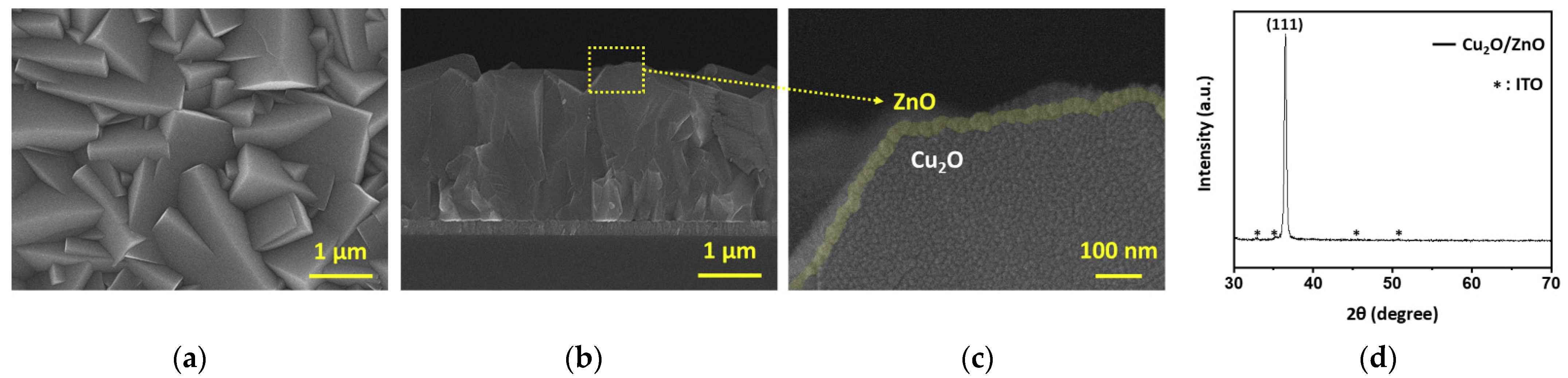
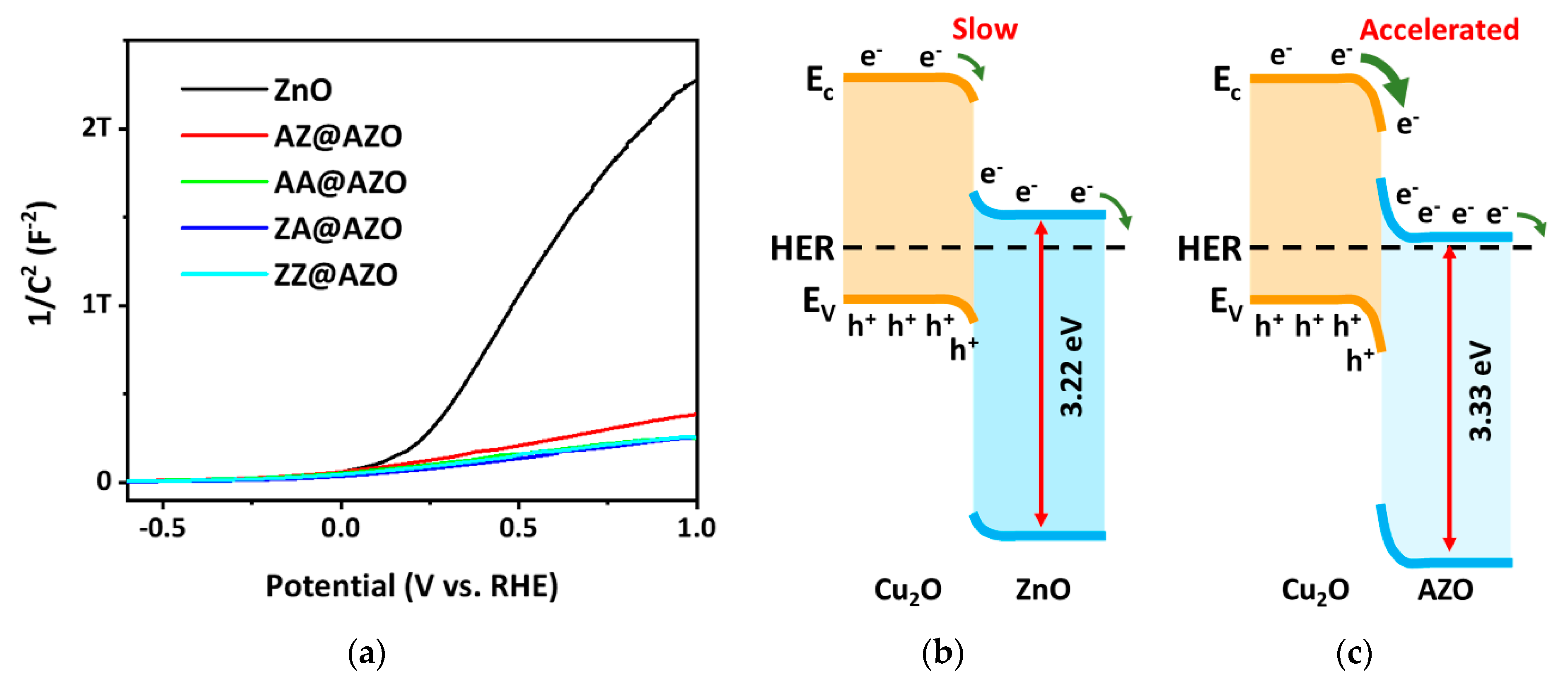
3.1. Characterization of Cu2O/ZnO and Cu2O/AZO Structures

To maximize the PEC performance of the p-type Cu2O photocathodes after the absorption of irradiated light, typical p-n heterojunctions with n-type overlayers can be employed. There are three key factors to be considered: (1) Ensuring the generation of EHPs with no degradation of the optical absorption efficiency of p-type Cu2O. This requires the use of transparent overlayers with wider bandgaps than those in Cu2O. (2) An adequate band alignment favored by the charge separation and charge transport behaviors in the heterojunction. (3) Suppressing the recombination loss of the charges transported from the Cu2O in the overlayers. These factors are strongly related to the electrical performance of n-type overlayers.
We selected general n-type ZnO-based overlayers (ZnO and AZO) and deposited them with a thickness of 20 nm using ALD. The details of the used overlayers are listed in Table 1. The typical morphology and phase of the Cu2O/ZnO heterojunction photocathodes prepared on ITO substrates were characterized by SEM, XRD, and UV-Vis-NIR absorbance spectra. Figure 1a shows the top view of the morphology of the Cu2O microcrystalline film after coating with 20-nm ZnO deposited at 423 K. Higher deposition temperatures induce the phase change of Cu2O into CuO, which severely degrades the PEC performance [20]. Because the ALD coating is typically homogeneous and there is no phase change at the used temperature, no apparent changes in the morphology of the microcrystals were detected in the samples before and after coating. As shown in the cross-sectional images in Figure 1b,c, the average thickness of the ZnO overlayers was approximately 20 nm, and the entire surface of the Cu2O was fully covered with ZnO, resulting in the prevention of direct contact between the photocathode and electrolyte. This leads to the effective suppression of photocorrosion on Cu2O and the formation of a uniform p-n junction. The XRD measurements revealed only Cu2O diffraction peaks in the Cu2O/ZnO sample (Figure 1d), except for ITO peaks. The absence of ZnO signals may be due to the small thickness and low crystallinity of the ZnO layers. It is necessary to accurately analyze the optical properties in order to check whether the ~20-nm-thick overlayers, formed on the surface of the absorption layer, affect the light absorption of the Cu2O layer.
It has been reported that doping with Al increases the bulk conductivity of the ZnO-based overlayers grown by ALD [32]. However, the stacking sequence of Al doping, such as the number and position, can significantly influence the electrical conductivity owing to the thin overlayer thickness. Nevertheless, detailed studies on the variation of the PEC performance of the photocathodes with respect to the Al doping stacking order are lacking. Figure 2 shows the visible-light absorbance of Cu2O, the overlayers, and the Cu2O/overlayer samples. The absorbance is converted from the transmittance of each sample by the Beer–Lambert Law, as shown in Equation (1) [33]:
A = −log(T)
where A is the absorbance and T is the transmittance. Additionally, the absorption coefficient α is calculated by the following Equation (2):
α = 2.303 A/d
where d is the film thickness.
The bandgaps can be estimated from Tauc’s plots using the absorption coefficient and transmittance, as shown in Equation (3) [34]:
α (hν) = C(hν−Eg)1/2
where α is the optical absorption coefficient, hν is the photon energy of the incident light, C is a constant, and Eg is the optical bandgap energy. The direct bandgap of the developed Cu2O was estimated to be 2.41 eV from the Tauc’s plot. The overlayers of the ZnO, AZ@AZO, AA@AZO, ZA@AZO, and ZZ@AZO thin films have bandgaps between 3.22 and 3.33 eV (Figure 2b, Table S1). The higher Al doping in the AZO films via the insertion of an additional Al layer induces a slight increase in the bandgap. This increase is ascribed to the Burstein–Moss effect, in which the increase in free-electron density causes an increased optical bandgap [28]. Fortunately, the very thin protective n-type overlayers on the surface of the electrodeposited Cu2O film did not induce any significant changes in the bandgap or absorbance spectra of the protected photoelectrodes (Figure 2c) compared to that of the pristine electrodeposited Cu2O. This implies that the use of these overlayers does not hinder the optical absorption of the photocathode Cu2O films, even though satisfactory p-n junctions were formed.

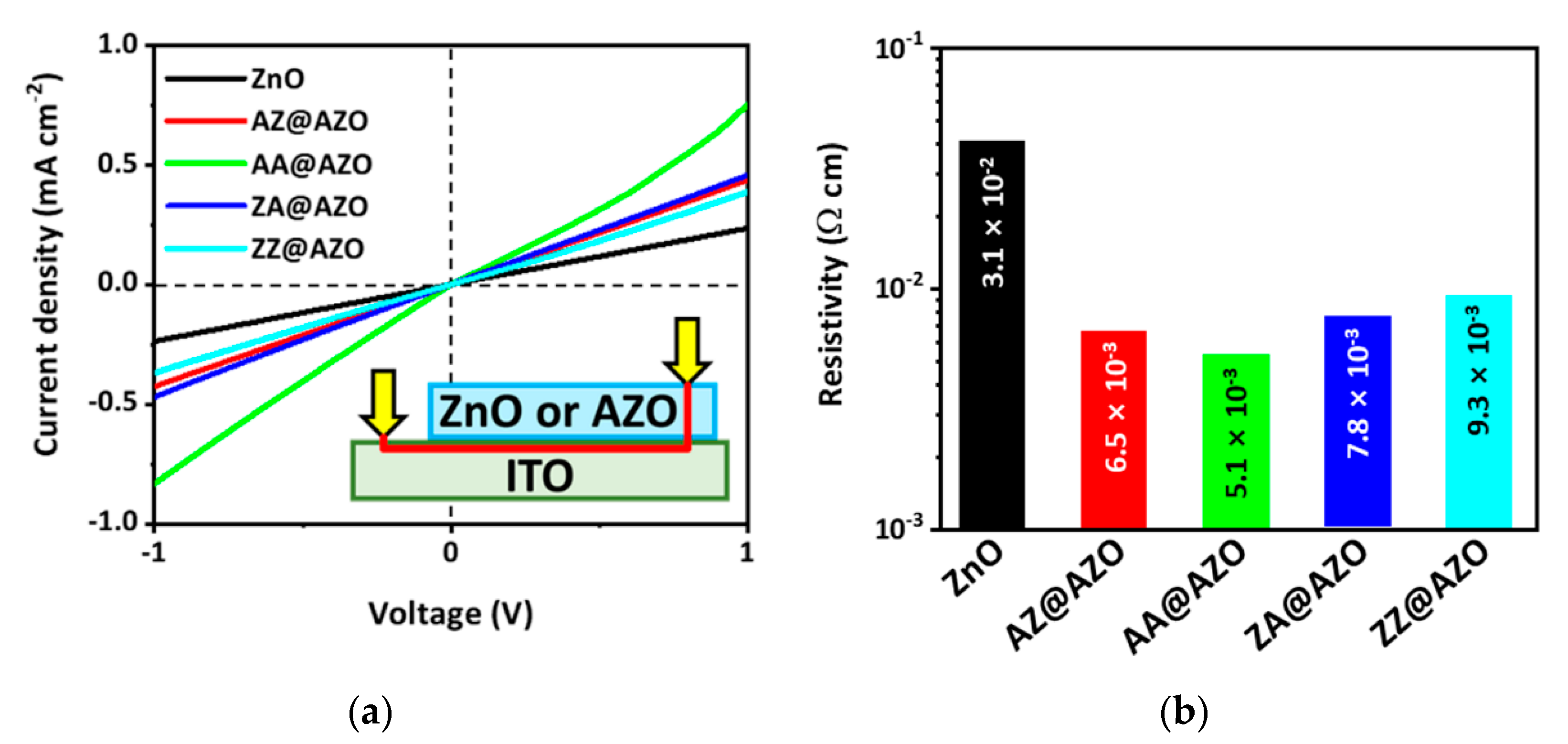
3.2. Electrical Characteristics of ZnO-Based Overlayers

The electron charges passing through the p-n heterojunction react with the electrolytes to produce hydrogen. Thus, it is necessary to track the path of the carriers in order to improve the photoelectrical reaction. The electrons transported along the conduction band of the Cu2O/overlayer heterojunction with an adequate band alignment can undergo recombination within the overlayers. This process is strongly related to the electrical conductivity and mobility of overlayers. Because the nominally undoped ZnO has a low electrical conductivity, it is expected to show a considerable loss in carrier transport. The selection of the first layers as well as the stacking sequence of the Al added as the electron donor via ALD should be investigated in detail for an optimal PEC operation. Thus, various ZnO-based overlayers were prepared with the same thickness (Table 1). Here, the AA@AZO and AZ@AZO samples utilize injected Al precursors as the first layer of the AZO coating, while the last layer for the AA@AZO and ZA@AZO samples is an Al monolayer. The electrical conductivities of the overlayers were compared with those of In-(Al)ZnO-ITO with a vertical stacking configuration (Figure 3a). All samples with Al doping exhibited an improved electrical conductivity, regardless of the stacking sequence. The lowest resistivity was obtained from the AA@AZO overlayer with Al monolayers in the bottom and top regions (Figure 3b). The AZ@AZO and ZA@AZO samples with one Al monolayer also showed better conductivity than the ZZ@AZO sample without any Al monolayer. This proves the effectiveness of using an Al monolayer in the bottom or top layers to improve the electrical conductivity.

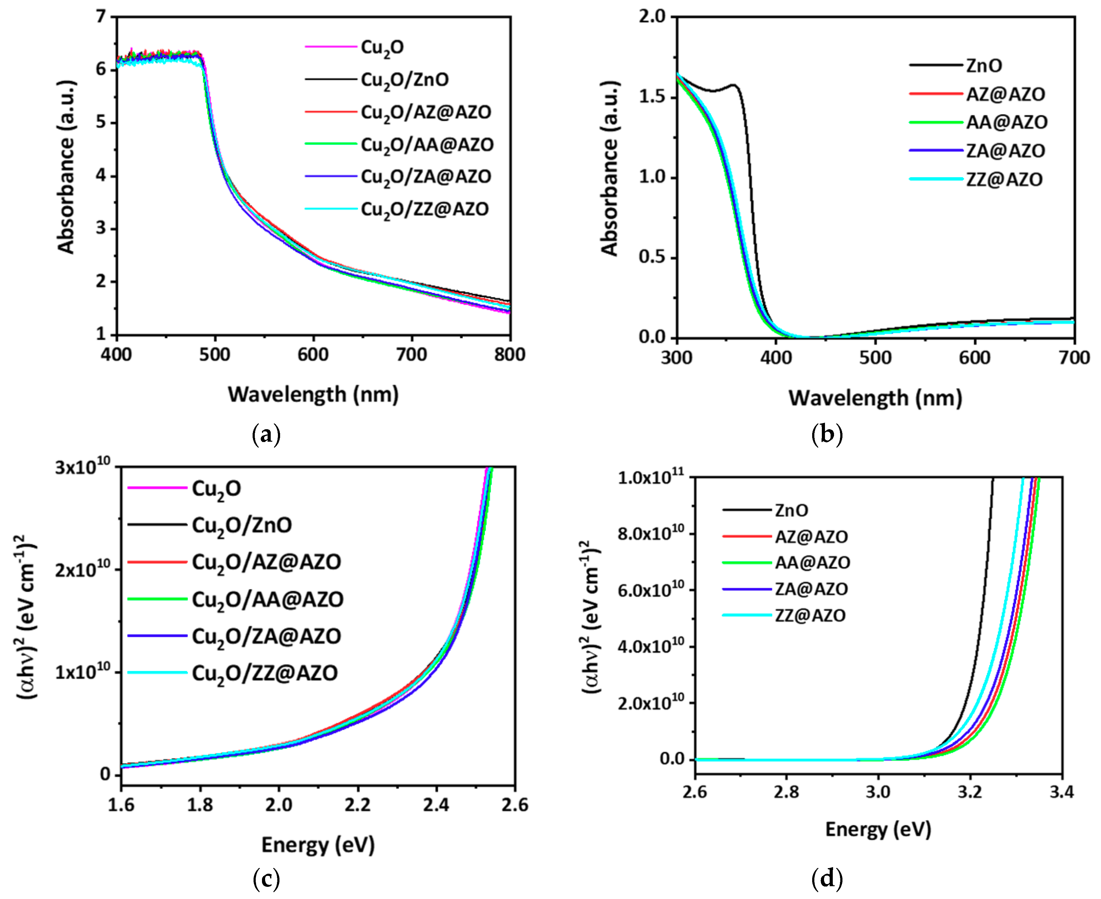
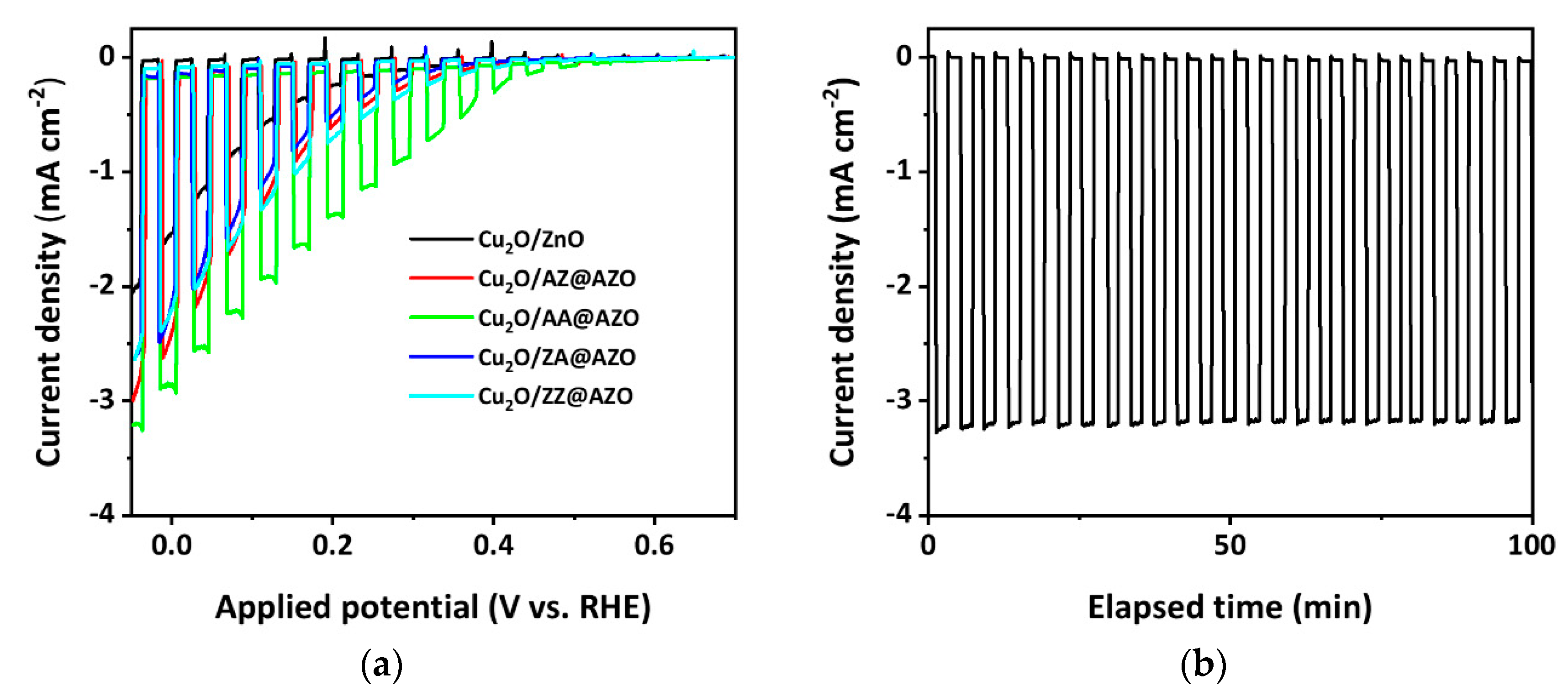
3.3. Visible-Light PEC Behavior of Samples with Different Overlayers

To confirm the improvement in the charge collection with the use of various overlayers, an electrochemical impedance spectroscopy (EIS) study was performed at 0 V vs. RHE to investigate the impedance at the Cu2O/overlayers’ interfaces under AM 1.5G illumination. The EIS curves are displayed in the form of a Nyquist plot in Figure 4, and an equivalent circuit is presented in Figure S1. In the equivalent circuit, R1 is the series resistance (including the resistance between ITO and Cu2O), R2 is the resistance of the Cu2O bulk and the charge transport through the overlayers, and R3 represents the resistance for the charge transfer at the interface with the electrolyte. C1 is the capacitance of the space charge region at the Cu2O/overlayer interfaces, and C2 is the surface space charge capacitance of the overlayers. C3 in the outermost shell is the capacitance of the electric double layer. Figure 4b shows that the photocathode with AA@AZO exhibited the lowest R1 among the prepared samples. The reduced C1 in Cu2O indicates that photocarriers generated in Cu2O were transported to the AA@AZO layers faster than in the other samples. Because AZ@AZO-overlayered Cu2O showed a similarly low R1 as AA@AZO-overlayered Cu2O, we found that the optimal p-n junction in the Cu2O surface was formed using AZO with an Al coating as the first monolayer. In addition, the lower R2 of AA@AZO-overlayered Cu2O implies that the AA@AZO layer has a higher conductivity than the other overlayers, which is in accordance with the results shown in Figure 3. Therefore, by depositing an AA@AZO overlayer on the surface of Cu2O, the transport efficiency can be considerably enhanced.
To investigate the reason behind the enhanced transport efficiency of AA@AZO-overlayered Cu2O, the carrier density and band structures were analyzed, and the results are shown in Figure 5. The photoactive Cu2O/AA@AZO electrodes were characterized by a Mott–Schottky analysis to evaluate the flat band potential (Vfb) and carrier density (NA) for band structure alignment. The Mott-Schottky plots of the ZnO and AZO single layers were analyzed using the following equation [35]:
C−2 = 2(eεε0NAA2)−1(V − VfbkBTe−1)
where C is the space charge capacitance, ε0 the permittivity of free space, ε the dielectric constant of ZnO and AZO (taken as 3.8) [36], e the elementary charge, A the electrode area, V the applied potential, T the temperature, and kB the Boltzmann constant. Compared with pure ZnO, there is an increase in the carrier density and a negative shift in the flat band potential in AZO overlayers (Figure 5a). As shown in Table S2, the AA@AZO overlayer shows a superior Vfb of −0.282 V vs. RHE and a high carrier density of 1.58 × 1018 cm−3. This doping behavior is demonstrated schematically in the band diagrams in Figure 5b,c. The use of the AA@AZO overlayer induces a relatively abrupt band bending at the Cu2O/AZO interface, which is expected to enhance charge transport because of the stronger built-in potential. The band structure of Cu2O has been described in a previous study [37].

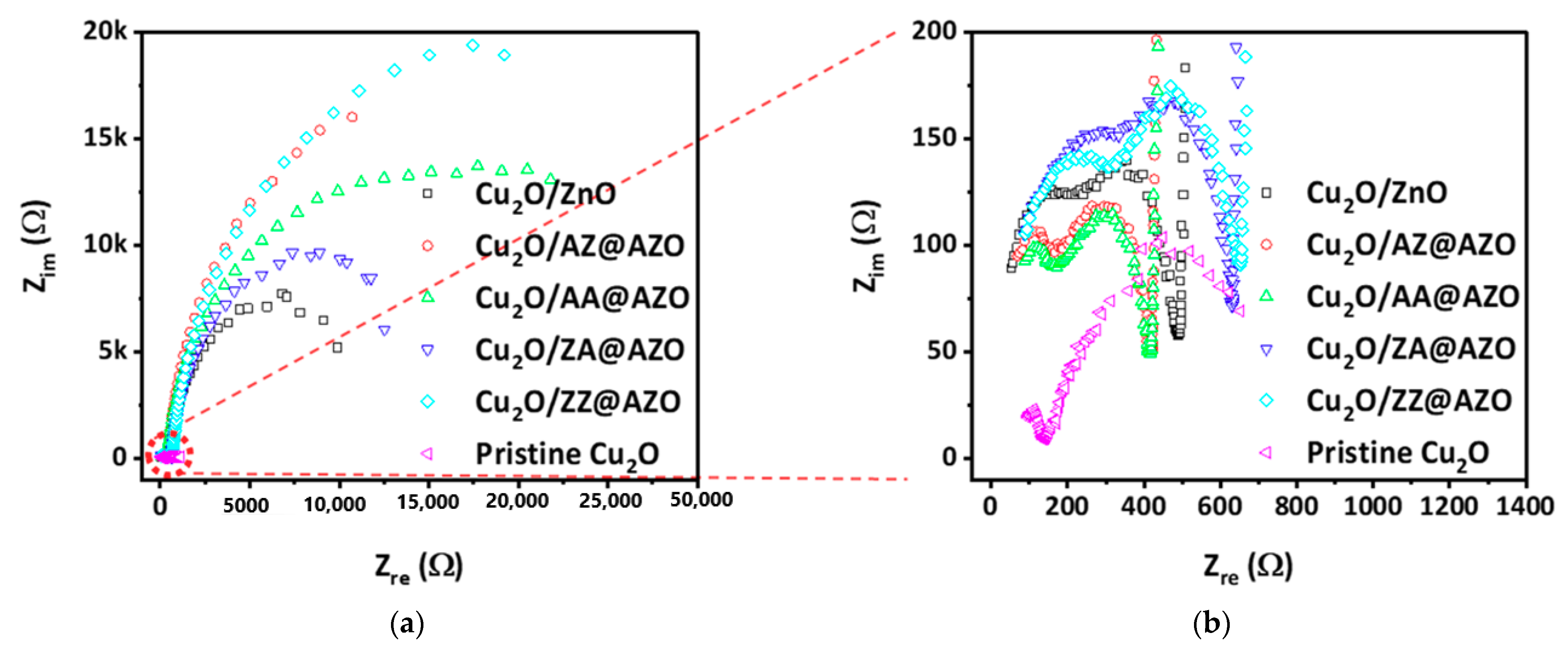
3.4. Enhancement in Charge Transfer and PEC Activity

To evaluate the photoelectrochemical performance of the Cu2O/overlayer photoelectrodes, linear sweep voltammetry (LSV) was conducted under AM 1.5G illumination. As shown in Figure 6a, the Cu2O/AZO electrodes show a better performance than the Cu2O/ZnO electrode with a current of > 1.6 mA cm−2 at 0 VRHE. Among various overlayers, the Cu2O/AA@AZO electrode exhibited the best open circuit potential (OCP) of 0.63 VRHE and a current density of –2.9 mA cm2 at 0 VRHE. This is consistent with the EIS and Mott-Schottky analyses. The AA@AZO layer has the lowest transport resistance among the samples and can induce a higher photovoltage and a lower flat band potential through the junction with Cu2O. In addition, Cu2O/AA@AZO exhibits a better fill factor than the other samples. To test the long-term stability of the Cu2O/AA@AZO electrode, a 20-nm TiO2 passivation layer and a Pt catalyst, respectively prepared by ALD and photoelectrochemical deposition, were deposited on the surface of AZO. From the chronoamperometry measurement at 0 VRHE, it can be seen that the Cu2O/AA@AZO/TiO2/Pt photoelectrode maintains a high cathodic photocurrent value of about −3.2 mA cm−2 for over 100 min.

4. Conclusions

We designed optimal AZO overlayers for Cu2O photocathodes with an enhanced charge transport and evaluated the properties of the AZO layers. The transparent ZnO and AZO, which have a wide bandgap of over 3.22 eV, suppressed the absorption of incident photons before they arrived at the Cu2O absorbing layers. The AZO layer has an increased bandgap (3.33 eV) due to the Al doping effect. By controlling the steps for Al injection during ALD, the AZO layers could be made to exhibit a higher electrical conductivity with increased Al doping. The Cu2O/AZO heterojunction generated a higher photovoltage via Al injection in the bottom and top regions of the AZO because of the enhanced built-in potential. The Cu2O/AA@AZO photoelectrode exhibited an optimal photocurrent of −3.2 mA cm−2 with TiO2 passivation and a Pt catalyst under AM 1.5G illumination.

Supplementary Materials

The following are available online at https://www.mdpi.com/2072-666X/12/3/338/s1, Figure S1: Equivalent circuit of Cu2O/overlayer photoelectrodes based on EIS study. Table S1: Band gap of overlayers estimated by Tauc plot. Table S2: Flat band potential and carrier density of overlayers estimated from the Mott–Schottky analysis.

Author Contributions

Conceptualization, H.H.L. and D.S.K.; methodology, D.S.K. and Y.B.K.; software, H.H.L. and H.W.S.; validation, S.S. and N.G.D.; formal analysis, H.H.L., D.S.K., and S.H.J.; investigation, H.H.L.; resources, J.H.C.; data curation, H.H.L. and D.S.K.; writing—original draft preparation, H.H.L. and D.S.K.; writing—review and editing, H.K.C.; visualization, H.H.L.; supervision, project administration, and funding acquisition, H.K.C. All authors have read and agreed to the published version of the manuscript.

Funding

This research was supported by the Basic Science Research Program through the National Research Foundation of Korea (NRF) funded by the Ministry of Education (No. 2019R1A6A1A03033215) and the Korea government (MSIT) (No.2021R1A2C3011870).

Institutional Review Board Statement

Not applicable.

Informed Consent Statement

Not applicable.

Data Availability Statement

Data available upon request from the corresponding author.

Conflicts of Interest

The authors declare no conflict of interest.

References

  1. Khaselev, O.; Turner, J.A. A Monolithic Photovoltaic-Photoelectrochemical Device for Hydrogen Production via Water Splitting. Science 1998, 280, 425–428. [Google Scholar] [CrossRef] [PubMed]
  2. Liu, R.; Zheng, Z.; Yang, X. Enhanced photoelectrochemical water-splitting performance of semiconductors by surface passivation layers. Energy Environ. Sci. 2014, 2504–2517. [Google Scholar] [CrossRef] [Green Version]
  3. Fujishima, A.; Honda, K. Electrochemical Photolysis of Water at a Semiconductor Electrode. Nature 1972, 238, 37–38. [Google Scholar] [CrossRef]
  4. Wang, G.; Wang, H.; Ling, Y.; Tang, Y.; Yang, X.; Fitzmorris, R.C.; Wang, C.; Zhang, J.Z.; Li, Y. Hydrogen-Treated TiO2 Nanowire Arrays for Photoelectrochemical Water Splitting. Nano Lett. 2011, 11, 3026–3033. [Google Scholar] [CrossRef]
  5. Brillet, J.; Yum, J.H.; Cornuz, M.; Hisatomi, T.; Solarska, R.; Augustynski, J.; Graetzel, M.; Sivula, K. Highly efficient water splitting by a dual-absorber tandem cell. Nat. Photonics 2012, 6, 824–828. [Google Scholar] [CrossRef]
  6. Dias, P.; Tânia, L.; Laura, M.; Luísa, A.; Adélio, M. Photoelectrochemical water splitting using WO3 photoanodes: The substrate and temperature roles. Phys. Chem. Chem. Phys. 2016, 18, 5232–5243. [Google Scholar] [CrossRef] [Green Version]
  7. Su, J.; Guo, L.; Bao, N.; Grimes, C.A. Nanostructured WO3/BiVO4 Heterojunction Films for Efficient Photoelectrochemical Water Splitting. Nano Lett. 2011, 11, 1928–1933. [Google Scholar] [CrossRef] [PubMed]
  8. Wang, S.; Chen, P.; Yun, J.; Hu, Y.; Wang, L. An Electrochemically Treated BiVO4 Photoanode for Efficient Photoelectrochemical Water Splitting. Angew. Chem. Int. Ed. 2017, 56, 8500–8504. [Google Scholar] [CrossRef] [PubMed] [Green Version]
  9. Hu, Y.; Kleiman-shwarsctein, A.; Forman, A.J.; Hazen, D.; Park, J.; Mcfarland, E.W. Pt-Doped α-Fe2O3 Thin Films Active for Photoelectrochemical Water Splitting. Chem. Mater. 2008, 20, 3803–3805. [Google Scholar] [CrossRef]
  10. Makimizu, Y.; Yoo, J.; Poornajar, M.; Nguyen, N.T.; Ahn, H.; Hwang, I.; Kment, S.; Schmuki, P. Effects of low oxygen annealing on the photoelectrochemical water splitting properties of α-Fe2O3. J. Mater. Chem. A 2020, 8, 1315–1325. [Google Scholar] [CrossRef]
  11. Hara, M.; Kondo, T.; Komoda, M.; Ikeda, S.; Shinohara, K.; Tanaka, A.; Kondo, J.N.; Domen, K. Cu2O as a photocatalyst for overall water splitting under visible light irradiation. Chem. Commun. 1998, 2, 357–358. [Google Scholar] [CrossRef]
  12. Lumley, M.A.; Radmilovic, A.; Jang, Y.J.; Lindberg, A.E.; Choi, K. Perspectives on the Development of Oxide-Based Photocathodes for Solar Fuel Production. J. Am. Chem. Soc. 2019, 141, 18358–18369. [Google Scholar] [CrossRef] [PubMed]
  13. Paracchino, A.; Laporte, V.; Sivula, K.; Grätzel, M.; Thimsen, E. Highly active oxide photocathode for photoelectrochemical water reduction. Nat. Mater. 2011, 10, 456–461. [Google Scholar] [CrossRef]
  14. Chen, D.; Liu, Z.; Guo, Z.; Yan, W.; Xin, Y. Enhancing light harvesting and charge separation of Cu2O photocathodes with spatially separated noble-metal cocatalysts towards highly efficient water splitting. J. Mater. Chem. A 2018, 6, 20393–20401. [Google Scholar] [CrossRef]
  15. Wang, T.; Wei, Y.; Chang, X.; Li, C.; Li, A.; Liu, S.; Zhang, J.; Gong, J. Homogeneous Cu2O p-n junction photocathodes for solar water splitting. Appl. Catal. B Environ. 2018, 226, 31–37. [Google Scholar] [CrossRef]
  16. Gerischer, H. On the stability of semiconductor electrodes against photodecomposition. J. Electroanal. Chem. 1977, 82, 133–143. [Google Scholar] [CrossRef]
  17. Paracchino, A.; Brauer, J.C.; Moser, J.; Thimsen, E.; Graetzel, M. Synthesis and Characterization of High-Photoactivity Electrodeposited Cu2O Solar Absorber by Photoelectrochemistry and Ultrafast Spectroscopy. J. Phys. Chem. C 2012, 116, 7341–7350. [Google Scholar] [CrossRef] [Green Version]
  18. Li, C.; Hisatomi, T.; Watanabe, O.; Nakabayashi, M.; Shibata, N.; Domen, K.; Delaunay, J.-J. Positive onset potential and stability of Cu2O-based photocathodes in water splitting by atomic layer deposition of a Ga2O3 buffer layer. Energy Environ. Sci. 2015, 8, 1493–1500. [Google Scholar] [CrossRef] [Green Version]
  19. Dai, P.; Li, W.; Xie, J.; He, Y.; Thorne, J.; McMahon, G.; Zhan, J.; Wang, D. Forming Buried Junctions to Enhance the Photovoltage Generated by Cuprous Oxide in Aqueous Solutions. Angew. Chem. Int. Ed. 2014, 53, 13493–13497. [Google Scholar] [CrossRef]
  20. Yang, Y.; Xu, D.; Wu, Q.; Diao, P. Cu2O/CuO Bilayered Composite as a High-Efficiency Photocathode for Photoelectrochemical Hydrogen Evolution Reaction. Sci. Rep. 2016, 6, 35158. [Google Scholar] [CrossRef] [Green Version]
  21. Paracchino, A.; Mathews, N.; Hisatomi, T.; Stefik, M.; Tilley, S.D.; Grätzel, M. Ultrathin films on copper(I) oxide water splitting photocathodes: A study on performance and stability. Energy Environ. Sci. 2012, 5, 8673–8681. [Google Scholar] [CrossRef]
  22. Kang, Z.; Yan, X.; Wang, Y.; Bai, Z.; Liu, Y.; Zhang, Z.; Lin, P.; Zhang, X.; Yuan, H.; Zhang, X.; et al. Electronic Structure Engineering Cu2O Film/ZnO Nanorods Array All-Oxide p-n Heterostructure for Enhanced Photoelectrochemical Property and Self-powered Biosensing Application. Sci. Rep. 2015, 5, 7882. [Google Scholar] [CrossRef] [Green Version]
  23. Eom, K.; Kim, S.; Lee, D.; Seo, H. Physicochemical interface effect in Cu2O–ZnO heterojunction on photocurrent spectrum. RSC Adv. 2015, 5, 103803–103810. [Google Scholar] [CrossRef]
  24. Tawfik, W.Z.; Hassan, M.A.; Johar, M.A.; Ryu, S.-W.; Lee, J.K. Highly conversion efficiency of solar water splitting over p-Cu2O/ZnO photocatalyst grown on a metallic substrate. J. Catal. 2019, 374, 276–283. [Google Scholar] [CrossRef]
  25. Musat, V.; Teixeira, B.; Fortunato, E.; Monteiro, R.C.C.; Vilarinho, P. Al-doped ZnO thin films by sol–gel method. Surf. Coat. Tech. 2004, 180–181, 659–662. [Google Scholar] [CrossRef]
  26. Kim, D.; Yun, I.; Kim, H. Fabrication of rough Al doped ZnO films deposited by low pressure chemical vapor deposition for high efficiency thin film solar cells. Curr. Appl. Phys. 2010, 10, S459–S462. [Google Scholar] [CrossRef]
  27. Park, K.C.; Ma, D.Y.; Kim, K.H. The physical properties of Al-doped zinc oxide films prepared by RF magnetron sputtering. Thin Solid Film. 1997, 305, 201–209. [Google Scholar] [CrossRef]
  28. Mass, J.; Bhattacharya, P.; Katiyar, R.S. Effect of high substrate temperature on Al-doped ZnO thin films grown by pulsed laser deposition. Mater. Sci. Eng. 2003, B103, 9–15. [Google Scholar] [CrossRef]
  29. George, S.M. Atomic Layer Deposition: An Overview. Chem. Rev. 2010, 110, 111–131. [Google Scholar] [CrossRef]
  30. Baek, S.K.; Kim, J.S.; Kim, Y.B.; Yoon, J.H.; Lee, H.; Cho, H.K. Dual Role of Sb-Incorporated Buffer Layers for High Efficiency Cuprous Oxide Photocathodic Performance: Remarkably Enhanced Crystallinity and Effective Hole Transport. ACS Sustain. Chem. Eng. 2017, 5, 8213–8221. [Google Scholar] [CrossRef]
  31. Kim, D.S.; Kim, Y.B.; Jung, S.H.; Deshpande, N.G.; Choi, J.H.; Lee, H.S.; Cho, H.K. Atomically tunable photo-assisted electrochemical oxidation process design for the decoration of ultimate-thin CuO on Cu2O photocathodes and their enhanced photoelectrochemical. J. Mater. Chem. A 2020, 21744–21755. [Google Scholar] [CrossRef]
  32. Nunes, P.; Fortunato, E.; Tonello, P.; Fernandes, F.B.; Vilarinho, P.; Martins, R. Effect of different dopant elements on the properties of ZnO thin films. Vacuum 2002, 64, 281–285. [Google Scholar] [CrossRef]
  33. Swinehart, D.F. The Beer-Lambert Law. J. Chem. Educ. 1962, 39, 333–335. [Google Scholar] [CrossRef]
  34. Tauc, J.; Grigorovici, R.; Vancu, A. Optical Properties and Electronic Structure of Amorphous Germanium. Phys. Stat. Sol. 1966, 15, 627–637. [Google Scholar] [CrossRef]
  35. Gelderman, K.; Lee, L.; Donne, S.W. Flat-Band Potential of a Semiconductor: Using the Mott–Schottky Equation. J. Chem. Educ. 2007, 84, 685–688. [Google Scholar] [CrossRef]
  36. Noh, H.; Scharrer, M.; Anderson, M.A.; Chang, R.P.H.; Cao, H. Photoluminescence modification by a high-order photonic band with abnormal dispersion in ZnO inverse opal. Phys. Rev. B 2008, 77, 115136. [Google Scholar] [CrossRef] [Green Version]
  37. Baek, S.K.; Kim, J.S.; Yun, Y.D.; Kim, Y.B.; Cho, H.K. Cuprous/Cupric Heterojunction Photocathodes with Optimal Phase Transition Interface via Preferred Orientation and Precise Oxidation. ACS Sustain. Chem. Eng. 2018, 6, 10364–10373. [Google Scholar] [CrossRef]
Figure 1. (a) Top view, (b,c) cross-view SEM images, and (d) X-ray diffraction pattern of the ZnO-overlayered Cu2O film.
Micromachines 12 00338 g001
Figure 2. (a,b) UV-Vis-NIR absorption spectra, and (c,d) Tauc plots of (a,c) pristine and overlayered Cu2O and (b,d) ZnO and AZO overlayers.
Micromachines 12 00338 g002
Figure 3. (a) I-V graphs of ZnO and AZO overlayers on ITO substrates; (b) Resistivity values from the 4-point probe method of 20-nm-thick ZnO and AZO thin films on glass substrates.
Micromachines 12 00338 g003
Figure 4. (a,b) Electrochemical impedance spectroscopy results of pristine Cu2O and Cu2O/overlayer electrodes under AM 1.5G illumination.
Micromachines 12 00338 g004
Figure 5. (a) Mott–Schottky plots of ZnO and AZO overlayers. Schematic band diagrams of the (b) Cu2O/ZnO and (c) Cu2O/AA@AZO junctions estimated from the Mott-Schottky plots.
Micromachines 12 00338 g005
Figure 6. (a) Linear sweep voltammetry properties of prepared Cu2O/overlayer photocathodes; (b) Long-term stability test of Cu2O/AA@AZO/TiO2/Pt photoelectrode at 0 VRHE in a 1 M Na2SO4 solution buffered with KH2PO4 and H3BO3 under AM 1.5G illumination.
Micromachines 12 00338 g006
Table 1. Nomenclature used for the prepared samples.
Sample (Cycle)Name
ZnO (20) × 5: 20 nmZnO
(Al (1) + ZnO (20)) × 5 (ZnO end): 20 nmAZ@AZO
(Al (1) + ZnO (20)) × 5 + Al (1) (Al end): 20 nmAA@AZO
(ZnO (20) + Al (1)) × 5 (Al end): 20 nmZA@AZO
(ZnO (20) + Al (1)) × 4 + (ZnO end): 20 nmZZ@AZO
Publisher’s Note: MDPI stays neutral with regard to jurisdictional claims in published maps and institutional affiliations.

