
Emulating Artificial Synaptic Plasticity Characteristics from SiO2-Based Conductive Bridge Memories with Pt Nanoparticles

 , and
, and 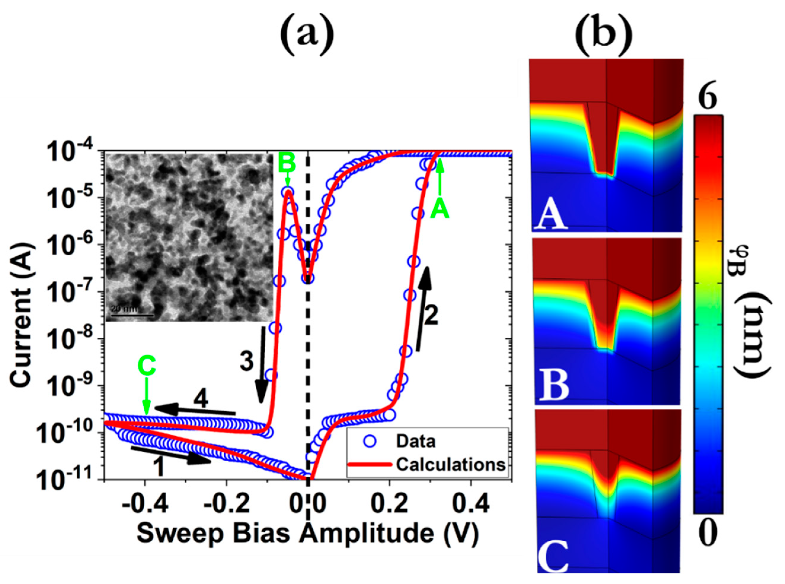
Abstract
:1. Introduction
2. Materials and Methods
3. Results
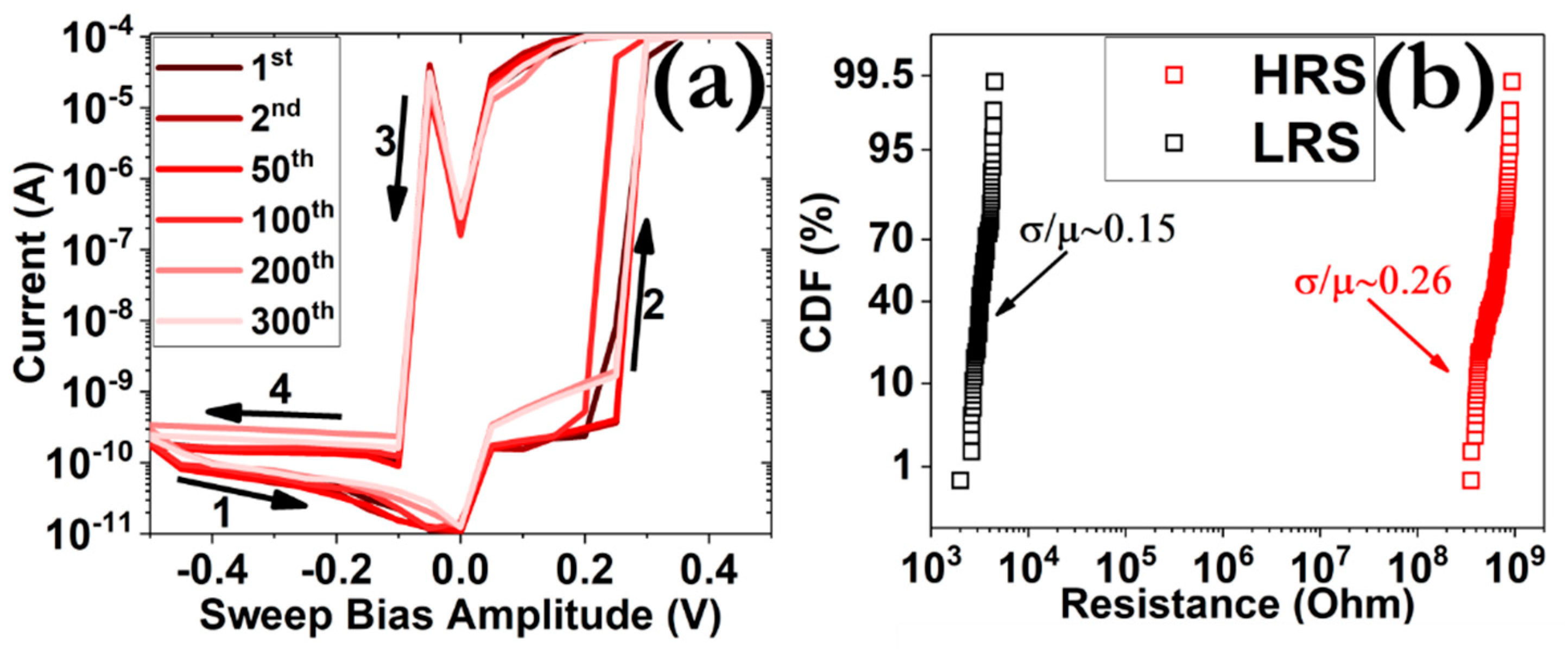
3.1. DC I–V Characteristics
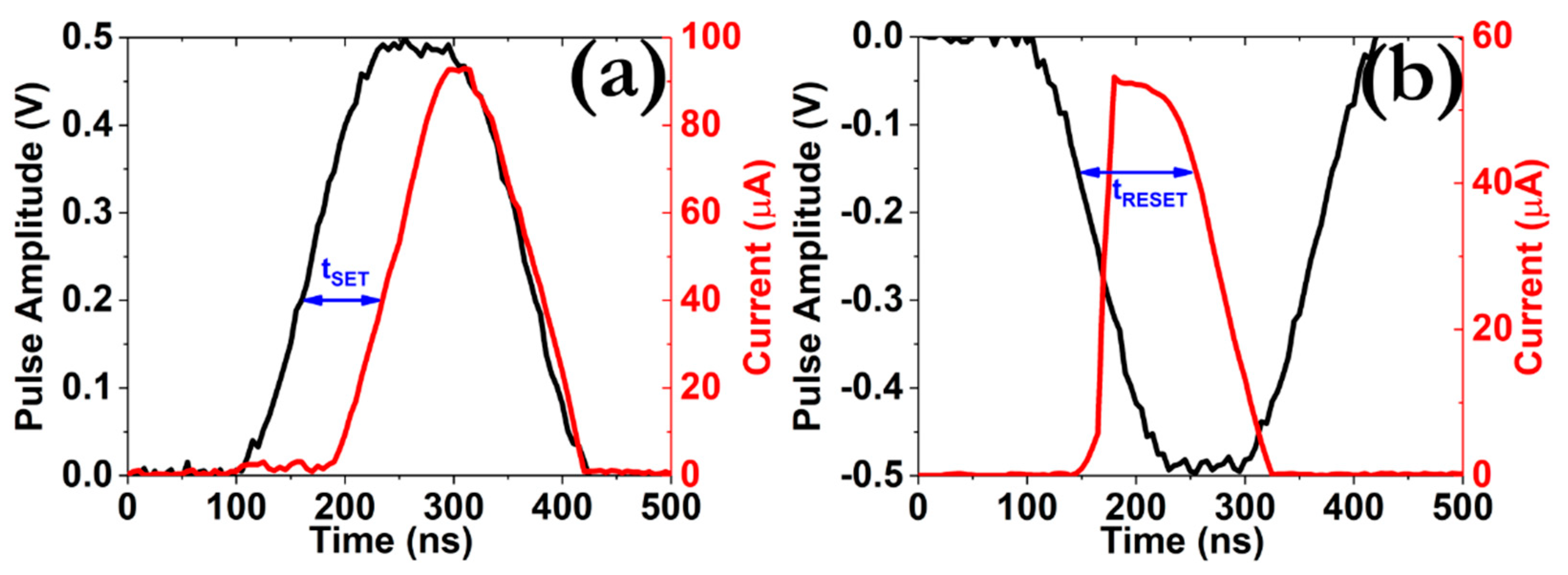
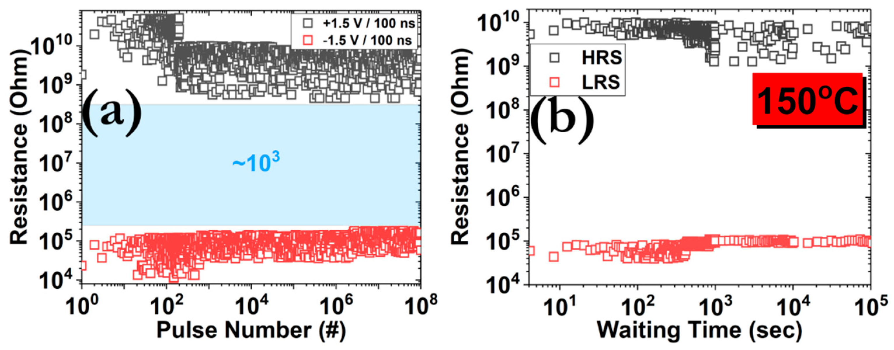
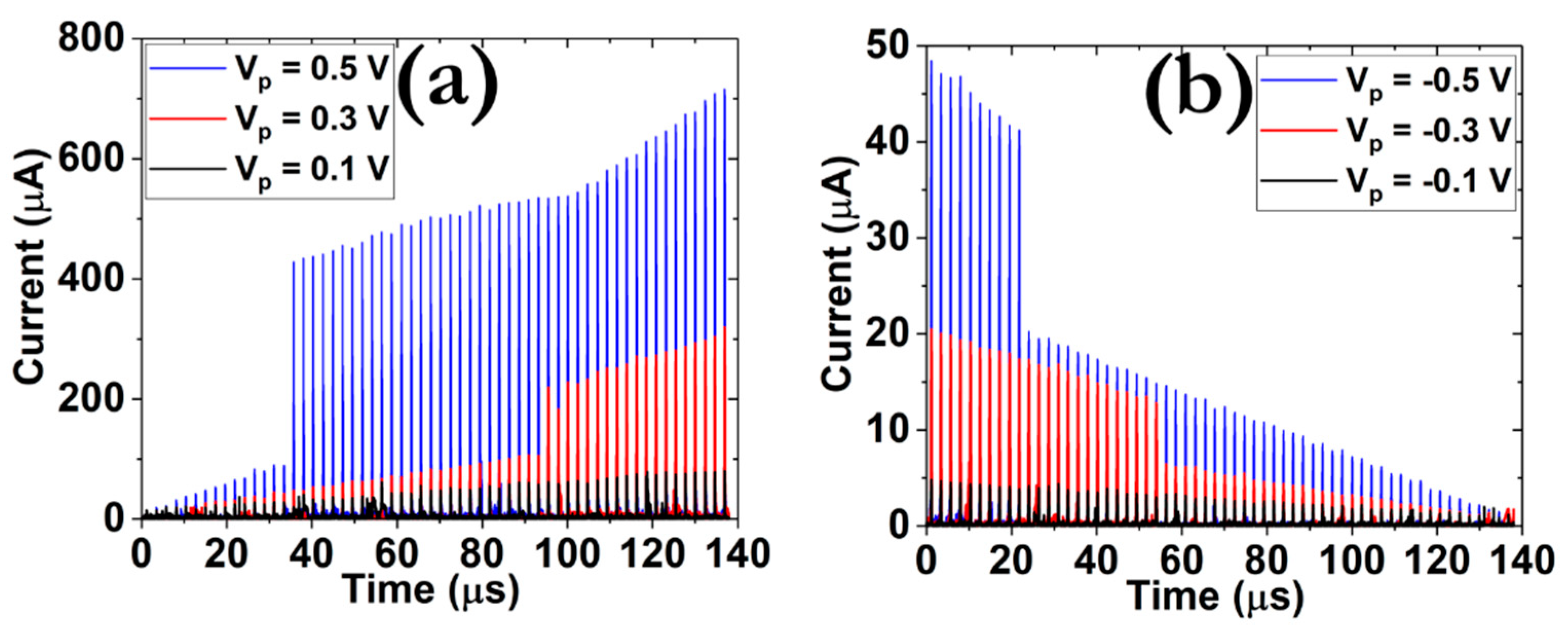
3.2. Pulsed I–V Characteristics
3.3. Analytical Modeling
3.4. Artificial Synaptic Activity
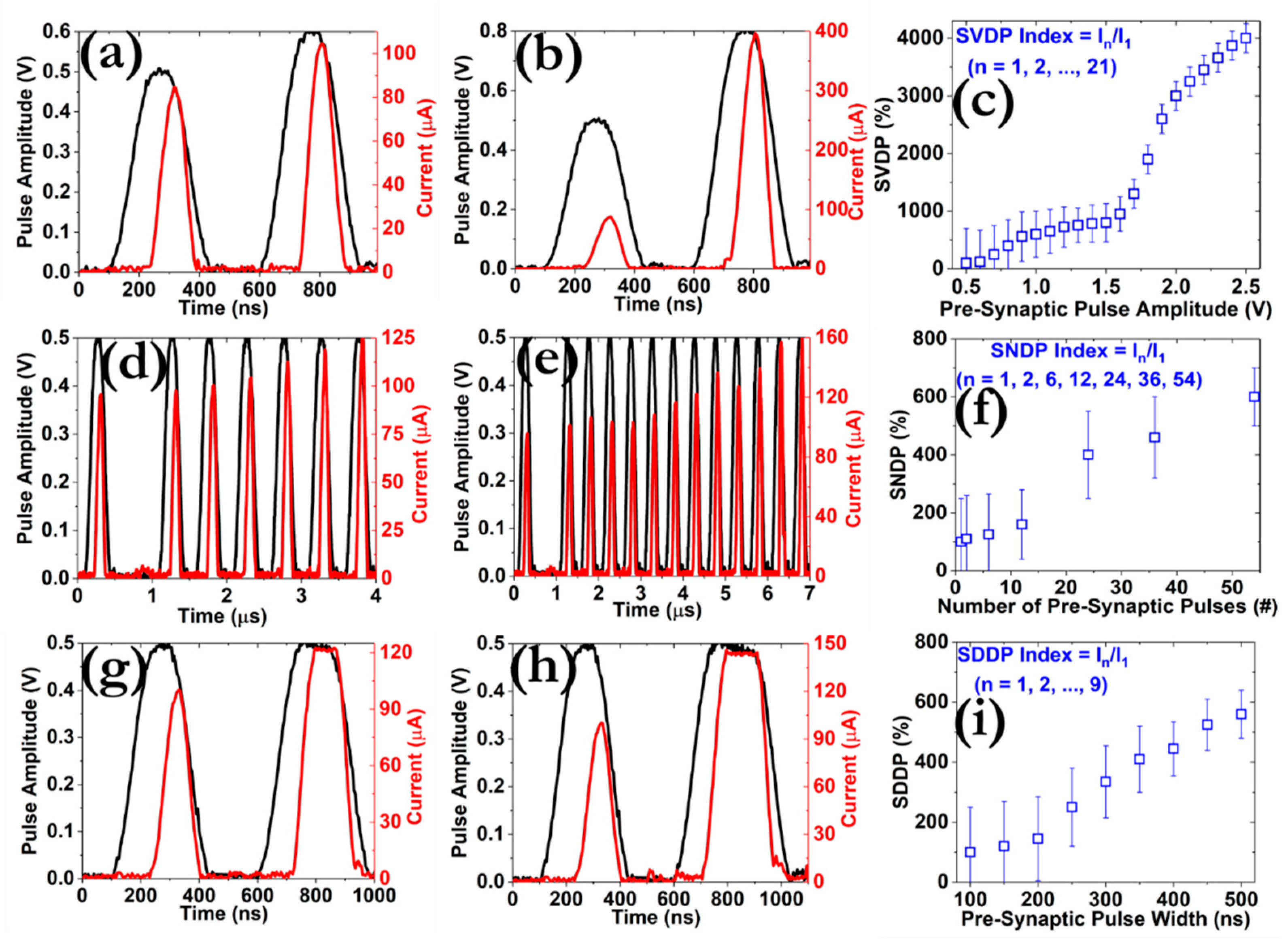
3.4.1. Potentiation and Depression Responses
3.4.2. STP and LTP Effects
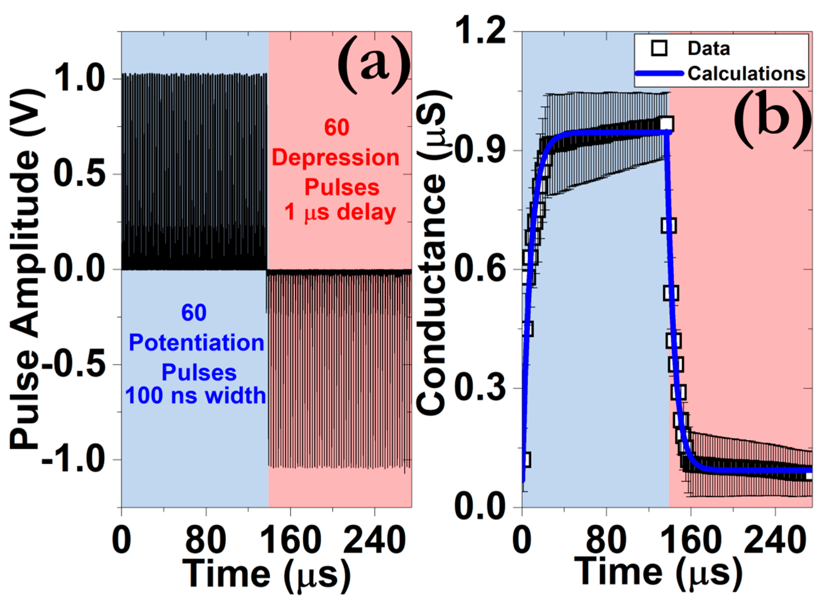
3.4.3. Synaptic Weight Modulation
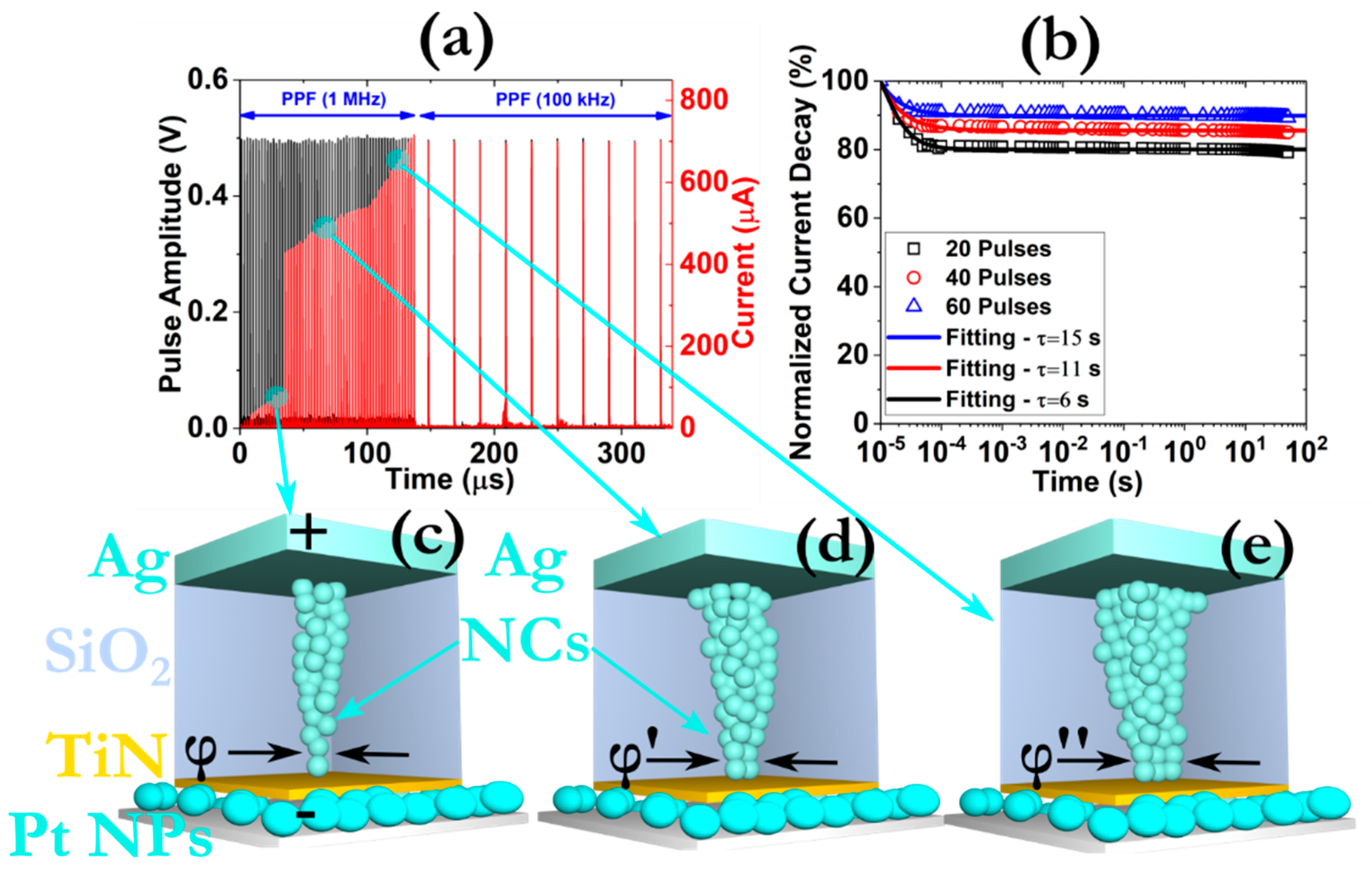
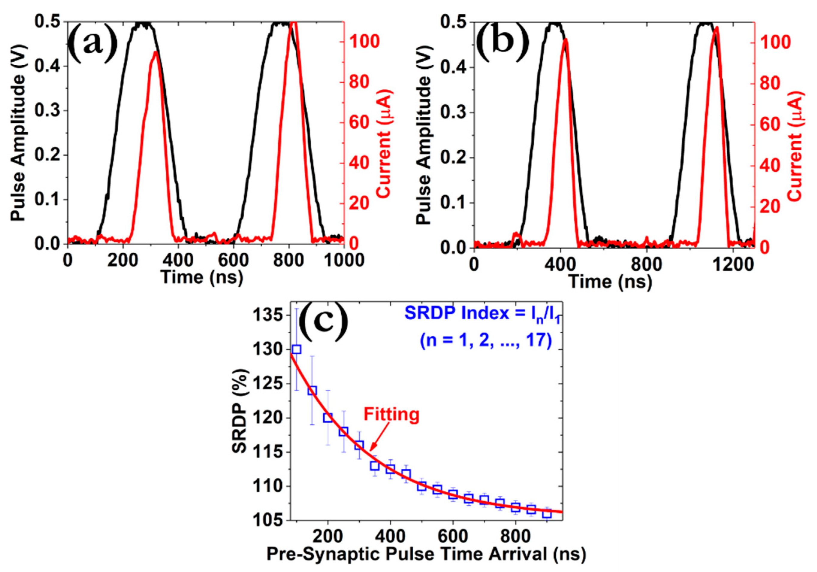
3.4.4. Spike-Dependent Plasticity Effects
4. Discussion
5. Conclusions
Supplementary Materials
Author Contributions
Funding
Data Availability Statement
Acknowledgments
Conflicts of Interest
References
- Amirsoleimani, A.; Alibart, F.; Yon, V.; Xu, J.; Pazhouhandeh, M.R.; Ecoffey, S.; Beilliard, Y.; Genov, R.; Drouin, D. In-Memory Vector-Matrix Multiplication in Monolithic Complementary Metal–Oxide–Semiconductor-Memristor Integrated Circuits: Design Choices, Challenges, and Perspectives. Adv. Intell. Syst. 2020, 2, 2000115. [Google Scholar] [CrossRef]
- Gupta, V.; Kapur, S.; Saurabh, S.; Grover, A. Resistive random access memory: A review of device challenges. IETE Tech. Rev. 2020, 37, 377–390. [Google Scholar] [CrossRef]
- Ielmini, D.; Amborgio, S. Emerging neuromorphic devices. Nanotechnology 2020, 31, 092001. [Google Scholar] [CrossRef]
- Huang, H.M.; Wang, Z.; Wang, T.; Xiao, Y.; Guo, X. Artificial Neural Networks Based on Memristive Devices: From Device to System. Adv. Intell. Syst. 2020, 2, 2000149. [Google Scholar] [CrossRef]
- Zhu, J.; Zhang, T.; Yang, Y.; Huang, R. A comprehensive review on emerging artificial neuromorphic devices. Appl. Phys. Rev. 2020, 7, 011312. [Google Scholar] [CrossRef]
- Nicholls, J.G.; Martin, A.R.; Fuchs, P.A.; Brown, D.A.; Diamond, M.E.; Weisblat, D.A. From Neuron to Brain, 5th ed.; Sinauer Associates: Sunderland, MA, USA, 2011; pp. 4–20. [Google Scholar]
- Kim, S.I.; Lee, Y.; Park, M.H.; Go, G.T.; Kim, Y.H.; Xu, W.; Lee, H.D.; Kim, H.; Seo, D.G.; Lee, W.; et al. Dimensionality Dependent Plasticity in Halide Perovskite Artificial Synapses for Neuromorphic Computing. Adv. Electron. Mater. 2019, 5, 1900008. [Google Scholar] [CrossRef]
- Zhu, X.; Du, C.; Jeong, Y.J.; Lu, W.D. Emulation of synaptic metaplasticity in Memristors. Nanoscale 2017, 9, 45. [Google Scholar] [CrossRef]
- Yang, Y.; Yin, M.; Yu, Z.; Wang, Z.; Zhang, T.; Cai, Y.; Lu, W.D.; Huang, R. Multifunctional Nanoionic Devices Enabling Simultaneous Heterosynaptic Plasticity and Efficient In-Memory Boolean Logic. Adv. Electron. Mater. 2017, 3, 1700032. [Google Scholar] [CrossRef]
- Tang, J.; Yuan, F.; Shen, X.; Wang, Z.; Rao, M.; He, Y.; Sun, Y.; Li, X.; Zhang, W.; Li, Y.; et al. Bridging Biological and Artificial Neural Networks with Emerging Neuromorphic Devices: Fundamentals, Progress, and Challenges. Adv. Mater. 2019, 31, 1902761. [Google Scholar] [CrossRef] [PubMed]
- Bousoulas, P.; Stathopoulos, S.; Tsialoukis, D.; Tsoukalas, D. Low–power and highly uniform 3–b multilevel switching in forming free TiO2-x-based RRAM with embedded Pt nanocrystals. IEEE Electron Device Lett. 2016, 37, 874–877. [Google Scholar] [CrossRef]
- Mehonic, A.; Shluger, A.L.; Gao, D.; Valov, I.; Miranda, E.; Ielmini, D.; Bricalli, A.; Ambrosi, E.; Li, C.; Yang, J.J.; et al. Silicon Oxide (SiOx): A Promising Material for Resistance Switching? Adv. Mater. 2018, 30, 1801187. [Google Scholar] [CrossRef] [PubMed] [Green Version]
- Ma, X.; Zhang, J.; Cai, W.; Wang, H.; Wilson, J.; Wang, Q.; Xin, Q.; Song, A. A Sputtered Silicon Oxide Electrolyte for High-Performance Thin-Film Transistors. Sci. Rep. 2017, 7, 1–6. [Google Scholar] [CrossRef] [PubMed] [Green Version]
- Kim, K.; Kim, S.; An, S.; Lee, G.H.; Kim, D.; Han, S. Anti-reflection porous SiO2 thin film deposited using reactive high-power impulse magnetron sputtering at high working pressure for use in a-Si:H solar cells. Sol. Energy Mater. Sol. Cells 2014, 130, 582–586. [Google Scholar] [CrossRef]
- Bousoulas, P.; Sakellaropoulos, D.; Papakonstantinopoulos, C.; Kitsios, S.; Arvanitis, C.; Bagakis, E.; Tsoukalas, D. Investigating the origins of ultra-short relaxation times of silver filaments in forming-free SiO2-based conductive bridge memristors. Nanotechnology 2020, 31, 454002. [Google Scholar] [CrossRef] [PubMed]
- Kobayashi, Y.; Zheng, W.; Chang, T.B.; Hirata, K.; Suzuki, R.; Ohdaira, T.; Ito, K. Nanoporous structure of sputter-deposited silicon oxide films characterized by positronium annihilation spectroscopy. J. Phys. D Appl. Phys. 2002, 91, 1704–1706. [Google Scholar] [CrossRef]
- Sakellaropoulos, D.; Bousoulas, P.; Papakonstantinopoulos, C.; Kitsios, S.; Tsoukalas, D. Spatial Confinement Effects of Embedded Nanocrystals on Multibit and Synaptic Properties of Forming Free SiO2-Based Conductive Bridge Random Access Memory. IEEE Electron Device Lett. 2020, 41, 1013–1016. [Google Scholar] [CrossRef]
- Liu, Q.; Long, S.; Lv, H.; Wang, W.; Niu, J.; Huo, Z.; Chen, J.; Liu, M. Controllable Growth of Nanoscale Conductive Filaments in Solid-Electrolyte-Based ReRAM by Using a Metal Nanocrystal Covered Bottom Electrode. ACS Nano 2010, 4, 6162–6168. [Google Scholar] [CrossRef]
- Fakhreddine, Z.; Lahbacha, K.; Melnikov, A.; Belgacem, H.; Magistris, M.; Dghais, W.; Maffucci, A. Signal and Thermal Integrity Analysis of 3-D Stacked Resistive Random Access Memories. IEEE Trans. Electron. Device 2021, 68, 88–94. [Google Scholar] [CrossRef]
- Sakellaropoulos, D.; Bousoulas, P.; Tsoukalas, D. Impact of Pt embedded nanocrystals on the resistive switching and synaptic properties of forming free TiO2 – x/TiO2 – y-based bilayer structures. J. Appl. Phys. 2019, 126, 044501. [Google Scholar] [CrossRef]
- Menzel, S.; Böttger, U.; Wimmer, M.; Salinga, M. Physics of the switching kinetics in resistive memories. Adv. Funct. Mater. 2015, 25, 6306–6325. [Google Scholar] [CrossRef]
- Lv, H.; Xu, X.; Sun, P.; Liu, H.; Luo, Q.; Liu, Q.; Banerjee, W.; Sun, H.; Long, S.; Li, L.; et al. Atomic View of Filament Growth in Electrochemical Memristive Elements. Sci. Rep. 2015, 5, 13311. [Google Scholar] [CrossRef] [Green Version]
- Onofrio, N.; Guzman, D.; Strachan, A. Atomic origin of ultrafast resistance switching in nanoscale electrometallization cells. Nat. Mat. 2015, 14, 440–446. [Google Scholar] [CrossRef] [PubMed]
- Cordero, G.G.; Roldan, J.B.; Molinos, F.J.; Suñé, J.; Long, S.; Liu, M. A new model for bipolar RRAMs based on truncated cone conductive filaments, a Verilog-A approach. Semicond. Sci. Technol. 2016, 31, 115013. [Google Scholar] [CrossRef]
- Sun, H.; Liu, Q.; Li, C.; Long, S.; Lv, H.; Bi, C.; Huo, Z.; Li, L.; Liu, M. Direct Observation of Conversion Between Threshold Switching and Memory Switching Induced by Conductive Filament Morphology. Adv. Funct. Mater. 2014, 24, 5679–5686. [Google Scholar] [CrossRef]
- Yang, Y.; Gao, P.; Gaba, S.; Chang, T.; Pan, X.; Lu, W. Observation of conducting filament growth in nanoscale resistive memories. Nat. Commun. 2012, 3, 732. [Google Scholar] [CrossRef] [PubMed]
- Wang, W.; Laudato, M.; Ambrosi, E.; Bricalli, A.; Covi, E.; Lin, Y.H.; Ielmini, D. Volatile Resistive Switching Memory Based on Ag Ion Drift/Diffusion Part I: Numerical Modeling. IEEE Trans. Electron Device 2019, 66, 3795–3801. [Google Scholar] [CrossRef]
- Zhao, Y.; Fang, C.; Zhang, X.; Xu, X.; Gong, T.; Luo, Q.; Chen, C.; Liu, Q.; Lv, H.; Li, Q.; et al. A compact model for drift and diffusion memristor applied in neuron circuits design. IEEE Trans. Electron Devices 2018, 65, 4290–4296. [Google Scholar] [CrossRef]
- Strukov, D.B.; Alibart, F.; Williams, R.S. Thermophoresis/diffusion as a plausible mechanism for unipolar resistive switching in metal–oxide–metal memristors. Appl. Phys. A 2012, 107, 509–518. [Google Scholar] [CrossRef]
- Samani, M.K.; Ding, X.Z.; Khosravian, N.; Ahmadi, B.A.; Yi, Y.; Chen, G.; Neyts, E.C.; Bogaerts, A.; Tay, B.K. Thermal conductivity of titanium nitride/titanium aluminum nitride multilayer coatings deposited by lateral rotating cathode arc. Thin Solid Films 2015, 578, 133–138. [Google Scholar] [CrossRef]
- Cheng, Z.; Liu, L.; Xu, S.; Lu, M.; Wang, X. Temperature Dependence of Electrical and Thermal Conduction in Single Silver Nanowire. Sci. Rep. 2015, 5, 10718. [Google Scholar] [CrossRef] [Green Version]
- Bousoulas, P.; Giannopoulos, I.; Asenov, P.; Karageorgiou, I.; Tsoukalas, D. Investigating the origins of high multilevel resistive switching in forming free Ti/TiO2−x-based memory devices through experiments and simulations. J. Appl. Phys. 2017, 121, 094501. [Google Scholar] [CrossRef]
- Meng, J.; Zhao, B.; Xu, Q.; Goodwill, J.M.; Bain, J.A.; Skowronski, M. Temperature overshoot as the cause of physical changes in resistive switching devices during electro-formation. J. Appl. Phys. 2020, 127, 235107. [Google Scholar] [CrossRef]
- Takeuchi, T.; Duszkiewicz, A.J.; Morris, R.G.M. The synaptic plasticity and memory hypothesis: Encoding, storage and persistence. Philos. Trans. R. Soc. B Biol. Sci. 2014, 369, 20130288. [Google Scholar] [CrossRef] [Green Version]
- Pereda, A.E. Electrical synapses and their functional interactions with chemical synapses. Nat. Rev. Neurosci. 2014, 15, 250. [Google Scholar] [CrossRef] [PubMed]
- Li, S.; Li, B.; Feng, X.; Chen, L.; Li, Y.; Huang, L.; Fong, X.; Ang, K.W. Electron-beam-irradiated rhenium disulfide memristors with low variability for neuromorphic computing. NPJ 2D Mater. Appl. 2021, 5, 1. [Google Scholar] [CrossRef]
- Xiong, W.; Zhu, L.Q.; Ye, C.; Yu, F.; Ren, Z.Y.; Ge, Z.Y. Bilayered Oxide-Based Cognitive Memristor with Brain-Inspired Learning Activities. Adv. Electron. Mater. 2019, 5, 1900439. [Google Scholar] [CrossRef]
- Shiffrin, R.M.; Atkinson, R.C. Storage and retrieval processes in long-term memory. Psychol. Rev. 1969, 76, 179. [Google Scholar] [CrossRef] [Green Version]
- Ohno, T.; Hasegawa, T.; Tsuruoka, T.; Terabe, K.; Gimzewski, J.K.; Aono, M. Short-term plasticity and long-term potentiation mimicked in single inorganic synapses. Nat. Mater. 2011, 10, 591. [Google Scholar] [CrossRef]
- Ilyas, N.; Li, D.; Li, C.; Jiang, X.; Jiang, Y.; Li, W. Analog Switching and Artificial Synaptic Behavior of Ag/SiOx:Ag/TiOx/p++-Si Memristor Device. Nanoscale Res. Lett. 2020, 15, 30. [Google Scholar] [CrossRef] [Green Version]
- Phillips, J.C. Stretched exponential relaxation in molecular and electronic glasses. Reports Prog. Phys. 1996, 59, 1133–1207. [Google Scholar] [CrossRef]
- Liu, Q.; Xue, Q.; Wang, Y.; Wei, X.; Hao, J. Bifunctional Device with High-Energy Storage Density and Ultralow Current Analog Resistive Switching. Adv. Electron. Mater. 2021, 7, 2000902. [Google Scholar] [CrossRef]
- Cho, H.; Kim, S. Emulation of Biological Synapse Characteristics from Cu/AlN/TiN Conductive Bridge Random Access Memory. Nanomaterials 2020, 10, 1709. [Google Scholar] [CrossRef]
- Cho, H.; Kim, S. Short-Term Memory Dynamics of TiN/Ti/TiO2/SiOx/Si Resistive Random Access Memory. Nanomaterials 2020, 10, 1821. [Google Scholar] [CrossRef]
- Wang, L.G.; Zhang, W.; Chen, Y.; Cao, Y.Q.; Li, A.D.; Wu, D. Synaptic Plasticity and Learning Behaviors Mimicked in Single Inorganic Synapses of Pt/HfOx/ZnOx/TiN Memristive System. Nanoscale Res. Lett. 2017, 12, 65. [Google Scholar] [CrossRef] [PubMed] [Green Version]
- Liu, H.; Wei, M.; Chen, Y. Optimization of non-linear conductance modulation based on metal oxide memristors. Nanotechnol. Rev. 2018, 7, 443–468. [Google Scholar] [CrossRef]
- Gokmen, T.; Onen, M.; Haensch, W. Training deep convolutional neural networks with resistive cross-point devices. Front Neurosci. 2017, 11, 538. [Google Scholar] [CrossRef]
- Xi, Y.; Gao, B.; Tang, J.; Chen, A.; Chang, M.F.; Hu, X.S.; Spiegel, J.; Qian, H.; Wu, H. In-Memory Learning With Analog Resistive Switching Memory: A Review and Perspective. Proc. IEEE 2020, 109, 14–42. [Google Scholar] [CrossRef]
- Yeon, H.; Lin, P.; Choi, C.; Tan, S.H.; Park, Y.; Lee, D.; Lee, J.; Xu, F.; Gao, B.; Wu, H.; et al. Alloying conducting channels for reliable neuromorphic computing. Nat. Nanotech. 2020, 15, 574–579. [Google Scholar] [CrossRef]
- Zhang, Y.; Wang, Z.; Zhu, J.; Yang, Y.; Rao, M.; Song, W.; Zhuo, Y.; Zhang, X.; Cui, M.; Shen, L.; et al. Brain-inspired computing with memristors: Challenges in devices, circuits, and systems. Appl. Phys. Rev. 2020, 7, 011308. [Google Scholar] [CrossRef]
- Min, S.Y.; Cho, W.J. Memristive Switching Characteristics in Biomaterial Chitosan-Based Solid Polymer Electrolyte for Artificial Synapse. Int. J. Mol. Sci. 2021, 22, 773. [Google Scholar] [CrossRef]
- Zucker, R.S.; Regehr, W.G. Short-Term Synaptic Plasticity. Annu. Rev. Physiol. 2002, 64, 355. [Google Scholar] [CrossRef] [PubMed] [Green Version]
- Xu, W.; Nguyen, T.L.; Kim, Y.T.; Wolf, C.; Pfattner, R.; Lopez, J.; Chae, B.G.; Kim, S.I.; Lee, M.Y.; Shin, E.Y.; et al. Ultrasensitive artificial synapse based on conjugated polyelectrolyte. Nano Energy 2018, 48, 575. [Google Scholar] [CrossRef] [Green Version]
- Gao, Q.; Huang, A.; Zhang, J.; Ji, Y.; Zhang, J.; Chen, X.; Geng, X.; Hu, Q.; Wang, M.; Xiao, Z.; et al. Artificial synapses with a sponge-like double-layer porous oxide memristor. NPG Asia Mater. 2021, 13, 3. [Google Scholar] [CrossRef]
- Bousoulas, P.; Panagopoulou, M.; Boukos, N.; Tsoukalas, D. Emulating artificial neuron and synaptic properties with SiO2-based memristive devices by tuning threshold and bipolar switching effects. J. Phys. D Appl. Phys. 2021, in press. [Google Scholar] [CrossRef]
- Sakellaropoulos, D.; Bousoulas, P.; Papakonstantinopoulos, C.; Kitsios, S.; Tsoukalas, D. Impact of Active Electrode on the Synaptic Properties of SiO₂-Based Forming-Free Conductive Bridge Memory. IEEE Trans. Electron. Device 2021, in press. [Google Scholar] [CrossRef]
- Simanjuntak, F.M.; Ohno, T.; Chandrasekaran, S.; Tseng, T.Y.; Samukawa, S. Neutral oxygen irradiation enhanced forming-less ZnO-based transparent analog memristor devices for neuromorphic computing applications. Nanotechnology 2020, 31, 26LT01. [Google Scholar] [CrossRef]
- Chandrasekaran, S.; Simanjuntak, F.M.; Panda, D.; Tseng, T.Y. Enhanced Synaptic Linearity in ZnO-Based Invisible Memristive Synapse by Introducing Double Pulsing Scheme. IEEE Trans. Electron. Devices 2019, 66, 4722–4726. [Google Scholar] [CrossRef]
- Simanjuntak, F.M.; Chandrasekaran, S.; Lin, C.C.; Tseng, T.Y. ZnO2/ZnO bilayer switching film for making fully transparent analog memristor devices. APL Mater. 2019, 7, 051108. [Google Scholar] [CrossRef] [Green Version]
- Lu, C.H.; Wong, G.M.T.; Deal, M.D.; Tsai, W.; Majhi, P.; Chui, C.O.; Visokay, M.R.; Chambers, J.J.; Colombo, L.; Clemens, B.M.; et al. Characteristics and Mechanism of Tunable Work Function Gate Electrodes Using a Bilayer Metal Structure on SiO2 and HfO2. IEEE Electron Device Lett. 2005, 26, 445–447. [Google Scholar]
- Bousoulas, P.; Karageorgiou, I.; Aslanidis, V.; Giannakopoulos, K.; Tsoukalas, D. Tuning Resistive, Capacitive, and Synaptic Properties of Forming Free TiO2-x-Based RRAM Devices by Embedded Pt and Ta Nanocrystals. Phys. Status Solidi A 2017, 1700440. [Google Scholar] [CrossRef]
- Li, Y.; Yin, L.; Wu, Z.; Li, X.; Song, X.; Gao, X.; Fu, L. Improved Resistive Switching Uniformity of SiO2 Electrolyte-Based Resistive Random Access Memory Device With Cu Oxidizable Electrode. IEEE Electron Device Lett. 2019, 40, 1599–1601. [Google Scholar] [CrossRef]
- Kuo, C.C.; Chen, I.C.; Shih, C.C.; Chang, K.C.; Huang, C.H.; Chen, P.H.; Chang, T.C.; Tsai, T.M.; Chang, J.S.; Huang, J.C. Galvanic Effect of Au–Ag Electrodes for Conductive Bridging Resistive Switching Memory. IEEE Electron Device Lett. 2015, 36, 1321–1324. [Google Scholar] [CrossRef]
- Xue, K.H.; Li, Y.; Su, H.L.; Yuan, J.H.; Li, Y.; Wang, Z.R.; Zhang, B.; Miao, X.S. Theoretical investigation of the Ag filament morphology in conductive bridge random access memories. J. Appl. Phys. 2018, 124, 152125. [Google Scholar] [CrossRef]
- Yang, Y.; Gao, P.; Li, L.; Pan, X.; Tappertzhofen, S.; Choi, S.; Waser, R.; Valov, I.; Lu, W.D. Electrochemical dynamics of nanoscale metallic inclusions in dielectrics. Nat. Commun. 2014, 5, 4232. [Google Scholar] [CrossRef] [Green Version]
- Goodwill, J.M.; Gala, D.K.; Bain, J.A.; Skowronski, M. Intrinsic current overshoot during thermal-runaway threshold switching events in TaOx devices. J. Appl. Phys. 2018, 123, 115105. [Google Scholar] [CrossRef]
- Avramescu, M.L.; Rasmussen, P.E.; Chénier, M.; Gardner, H.D. Influence of pH, particle size and crystal form on dissolution behaviour of engineered nanomaterials. Environ. Sci. Pollut. Res. Int. 2017, 24, 1553–1564. [Google Scholar] [CrossRef] [Green Version]
- Nanda, K.K.; Sahu, S.N.; Behera, S.N. Liquid-drop model for the size-dependent melting of low-dimensional systems. Phys. Rev. A 2002, 66, 013208. [Google Scholar] [CrossRef]
- Asoro, M.A.; Damiano, J.; Ferreira, P.J. Size Effects on the Melting Temperature of Silver Nanoparticles: In-situ TEM Observations. Microsc. Microanal. 2009, 15, 706–707. [Google Scholar] [CrossRef] [Green Version]
- Luo, W.; Hu, W.; Xiao, S. Size Effect on the Thermodynamic Properties of Silver Nanoparticles. J. Phys. Chem. C 2008, 112, 2359–2369. [Google Scholar] [CrossRef]
- Sheny, D.S.; Philip, D.; Mathew, J. Synthesis of platinum nanoparticles using dried Anacardium occidentale leaf and its catalytic and thermal applications. Spectrochim. Acta Part A Mol. Biomol. Spectrosc. 2013, 114, 267–271. [Google Scholar] [CrossRef] [PubMed]
- Lacy, F. Using Nanometer Platinum Films as Temperature Sensors (Constraints From Experimental, Mathematical, and Finite-Element Analysis). IEEE Sens. J. 2009, 9, 1111–1117. [Google Scholar] [CrossRef]
- Chang, S.H.; Chae, S.C.; Lee, S.B.; Liu, C.; Noh, T.W.; Lee, J.S.; Kahng, B.; Jang, J.H.; Kim, M.Y.; Kim, D.W.; et al. Effects of heat dissipation on unipolar resistance switching in Pt∕NiO∕Pt capacitors. Appl. Phys. Lett. 2008, 92, 183507. [Google Scholar] [CrossRef] [Green Version]


Publisher’s Note: MDPI stays neutral with regard to jurisdictional claims in published maps and institutional affiliations. |
© 2021 by the authors. Licensee MDPI, Basel, Switzerland. This article is an open access article distributed under the terms and conditions of the Creative Commons Attribution (CC BY) license (http://creativecommons.org/licenses/by/4.0/).
Share and Cite
Bousoulas, P.; Papakonstantinopoulos, C.; Kitsios, S.; Moustakas, K.; Sirakoulis, G.C.; Tsoukalas, D. Emulating Artificial Synaptic Plasticity Characteristics from SiO2-Based Conductive Bridge Memories with Pt Nanoparticles. Micromachines 2021, 12, 306. https://doi.org/10.3390/mi12030306
Bousoulas P, Papakonstantinopoulos C, Kitsios S, Moustakas K, Sirakoulis GC, Tsoukalas D. Emulating Artificial Synaptic Plasticity Characteristics from SiO2-Based Conductive Bridge Memories with Pt Nanoparticles. Micromachines. 2021; 12(3):306. https://doi.org/10.3390/mi12030306
Chicago/Turabian StyleBousoulas, Panagiotis, Charalampos Papakonstantinopoulos, Stavros Kitsios, Konstantinos Moustakas, Georgios Ch. Sirakoulis, and Dimitris Tsoukalas. 2021. "Emulating Artificial Synaptic Plasticity Characteristics from SiO2-Based Conductive Bridge Memories with Pt Nanoparticles" Micromachines 12, no. 3: 306. https://doi.org/10.3390/mi12030306