Article

Large-Signal Linearity and High-Frequency Noise of Passivated AlGaN/GaN High-Electron Mobility Transistors

Department of Materials Science and Engineering, National Dong Hwa University, 1, Sec. 2, Da Hsueh Rd., Shou-Feng, Hualien 974, Taiwan
*
Author to whom correspondence should be addressed.
Micromachines 2021, 12(1), 7; https://doi.org/10.3390/mi12010007
Submission received: 19 November 2020 / Revised: 15 December 2020 / Accepted: 21 December 2020 / Published: 24 December 2020
(This article belongs to the Special Issue GaN-Based Semiconductor Devices)

Abstract

:
This study proposes AlGaN/GaN/silicon high-electron mobility transistors (HEMTs) grown by a metallorganic chemical vapor deposition (MOCVD) system. The large-signal linearity and high-frequency noise of HEMTs without and with different passivation layers are compared. The experimental data show that the addition of a TiO2 passivation layer to undoped AlGaN/GaN HEMT’s increases the value of the third-order intercept point (OIP3) by up to 70% at 2.4 GHz. Furthermore, the minimum noise figure (NFmin) of the HEMT with TiO2 passivation is significantly reduced.

1. Introduction

Heterostructure field-effect transistor (HFET) technology has become essential in microwave communication systems [1,2]. III-nitride high-electron-mobility transistors (HEMTs) are of significant importance in the development of next-generation power applications [3,4,5]. The AlGaN/GaN heterostructure has the advantage of large electron velocity and high breakdown electric field. Furthermore, the polar properties of the AlGaN/GaN heterojunction allows the formation of two-dimensional electron gas (2DEG). Even without intentional doping, the 2DEG concentrations of the AlGaN/GaN HEMTs is as high as the order of 1013 cm−2.
Many passivation materials have been investigated to effectively passivate the surface of AlGaAs/InGaAs [6] and InAlAs/InGaAs/InP [7] HEMTs by using either a wet or dry process. The performance of AlGaN/GaN HEMT technology is limited by charge trapping effects. Consequently, various candidates for passivation has been attempted to neutralize the net surface charge arising from the combination of surface states and the polarized barrier [8,9,10,11,12,13,14,15,16,17,18]. Most works focus on the performance of the passivated AlGaN/GaN HEMTs at room temperature. The room-temperature characteristics of AlGaN/GaN HEMT with HfO2 and TiO2 passivation were reported [11]. However, AlGaN/GaN heterostructure is a promising material system for high-temperature electronics. HEMTs that can operate at high temperatures are helpful in broad extent of applications [13,19]. Consequently, the high-temperature characteristics of the passivated AlGaN/GaN HEMTs are measured herein. Furthermore, the linearity in power amplifier is important when we move towards the fifth generation (5 G) wireless systems. Increasing the linearity of HEMTs can supply many advantages at the system level. Consequently, the large-signal linearity of the passivated AlGaN/GaN HEMTs are also studied. To the best of the authors’ knowledge, there has not been a comparison of the large-signal linearity and noise figure for the AlGaN/GaN HEMTs with HfO2 and TiO2 passivation. Experimental results demonstrate the high-performance passivated HEMT with stable operation at elevated temperatures up to 420 K. The measured large-signal linearity and high-frequency noise of the passivated HEMT are better than for the identical geometry unpassivated HEMT.

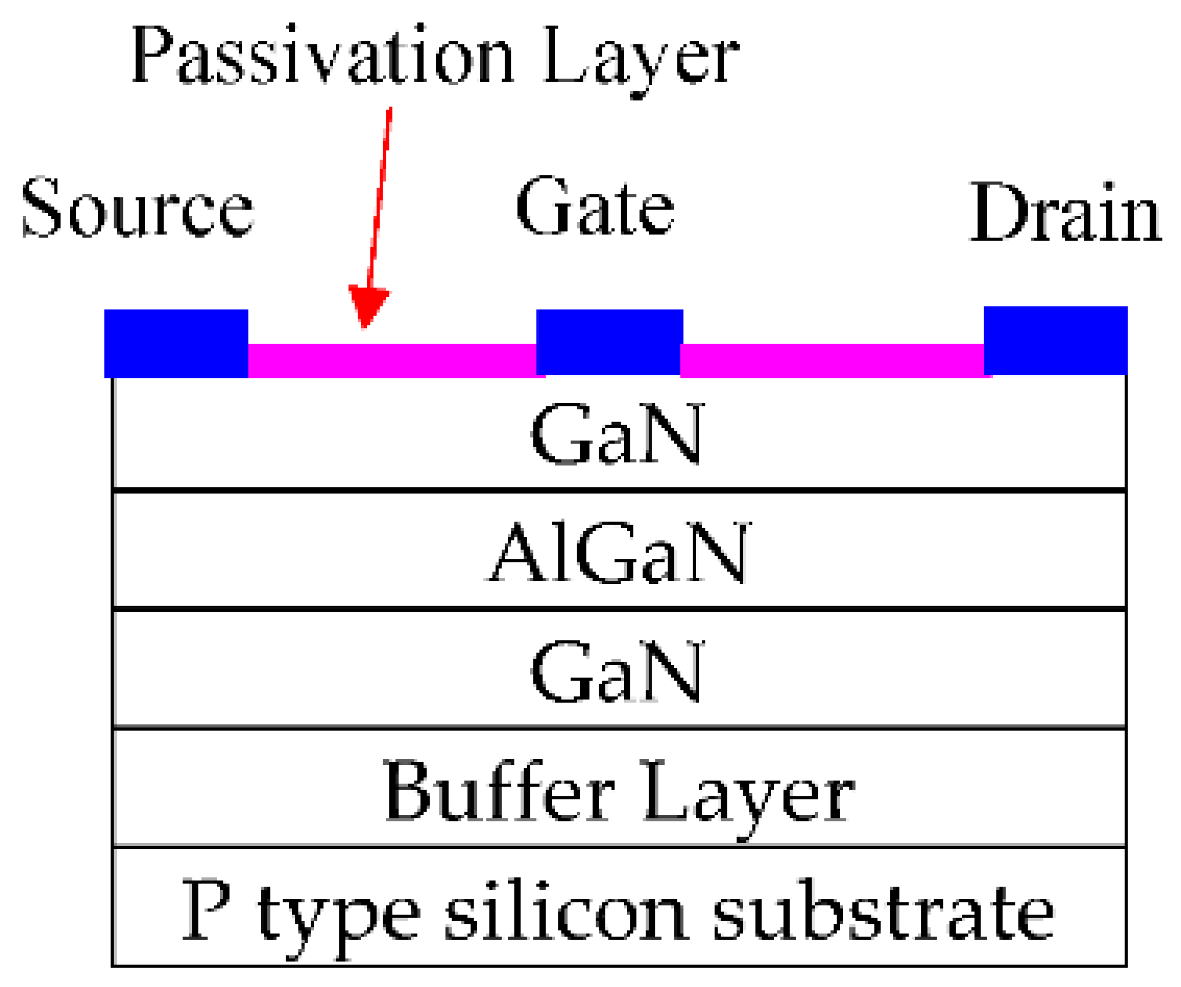
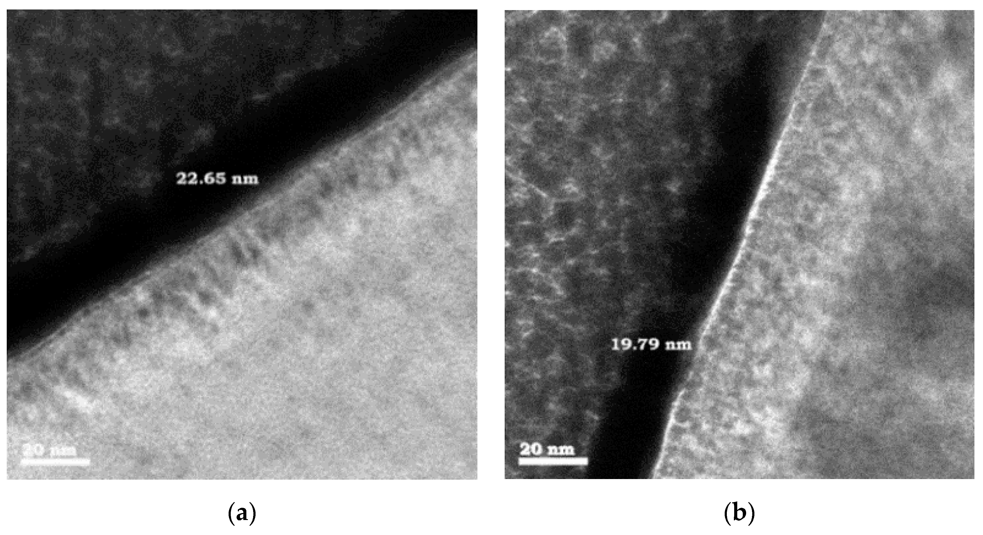
2. Device Structure and Experiments

The studied devices were built on silicon substrate with epilayers that were grown by metal-organic chemical vapor deposition (MOCVD). The layer structure of the HEMT is as follows. First, a buffer was grown, followed by an undoped GaN. Then, 30 nm undoped Al0.26Ga0.74N layer was formed and capped by a 2 nm GaN layer.
Mesa etching was employed to achieve device isolation. Ti/Al/Au ohmic contacts for the source and drain electrodes were deposited. The gate metallization involved Ni, capped with Au. The HEMT without passivation is the reference HEMT. In our study, the HEMT with HfO2 passivation is referred to as HfO2-HEMT. The HEMTs with TiO2 passivation is referred to as TiO2-HEMT. The TiO2 film was sputtered in a sputtering system using a three-inch high-purity target of titanium dioxide in a mixture of argon and oxygen gas. HfO2 film was sputtered using hafnium dioxide. Figure 1 displays the layer structure of the studied HEMTs with passivation. The cross section of the passivated HEMTs was investigated by a transmission electron microscopy (TEM) (JEOL Co., Tokto, Japan). The probe station was fitted with a heated device stage. The DC characteristics of the HEMTs were measured with a Keithley 4200 semiconductor characterization system (Tektronix, Beaverton, OR, USA). The field-effect transistor had a gate length of 1 μm. The gate-to-drain spacing was 2 μm. The gate-to-source spacing was also 2 μm.

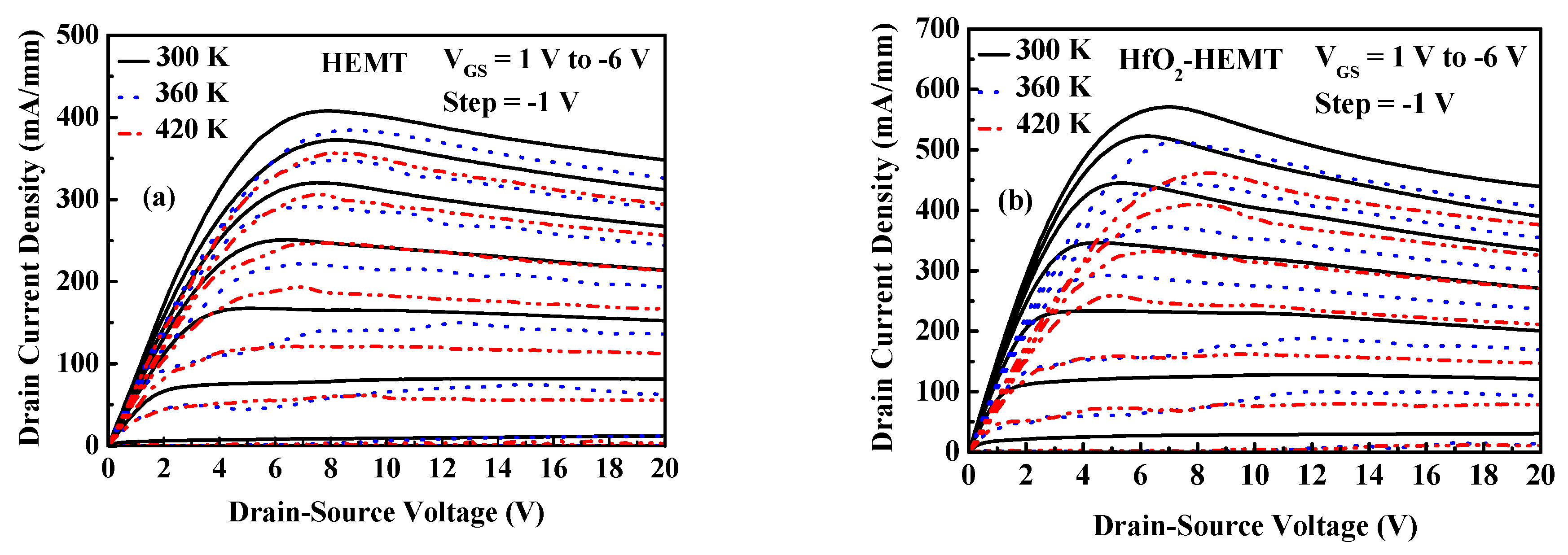
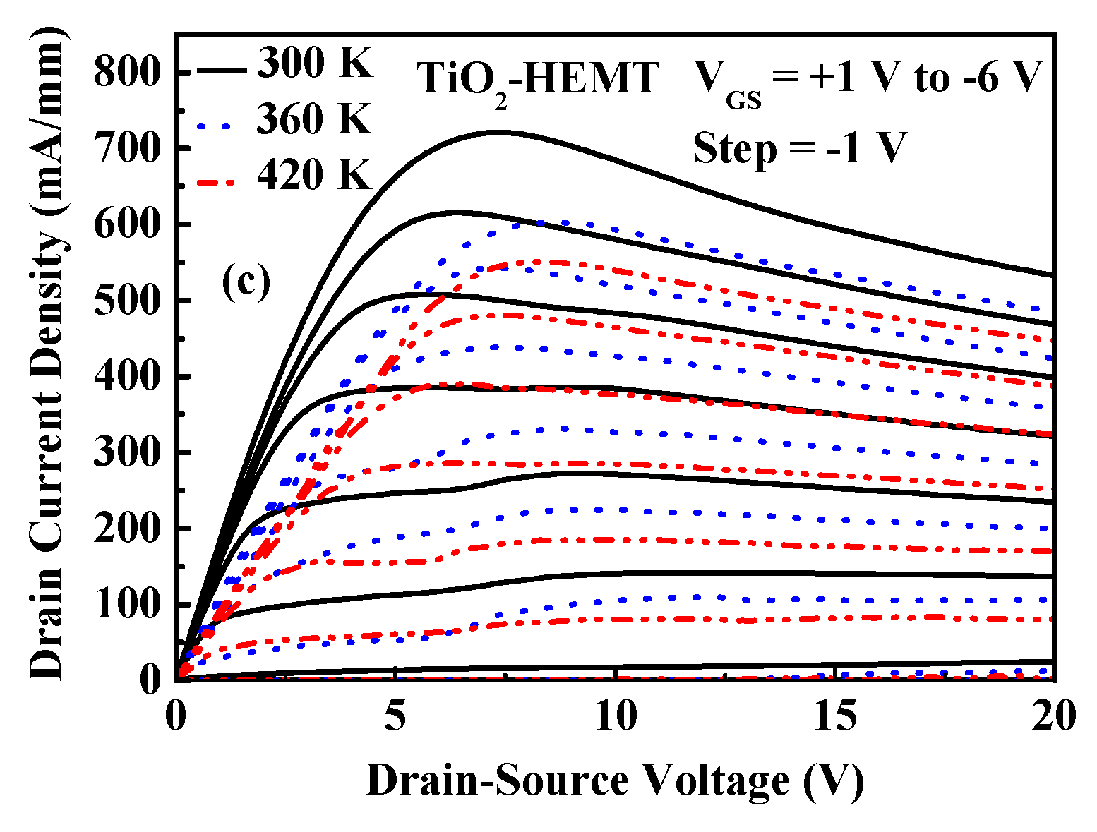
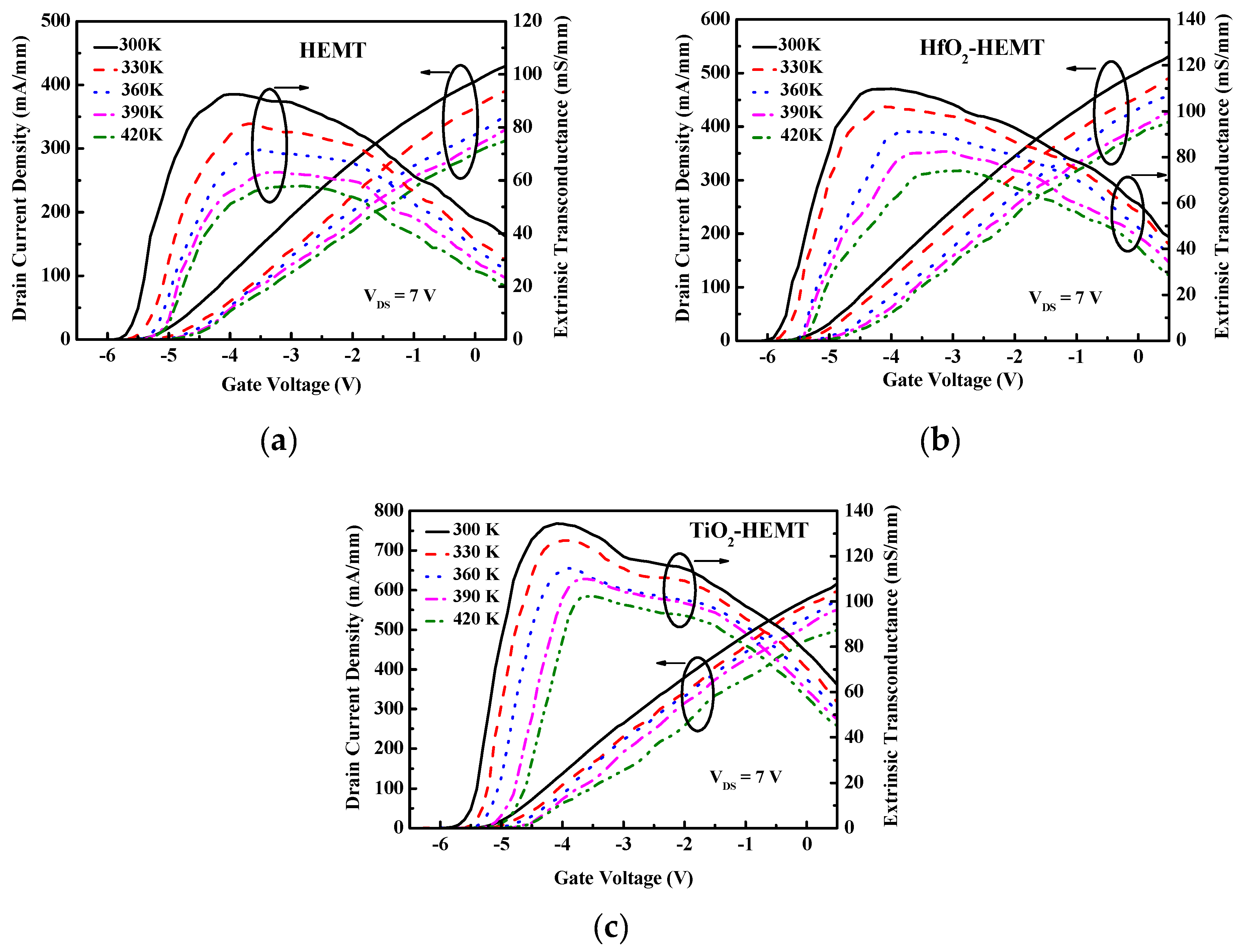
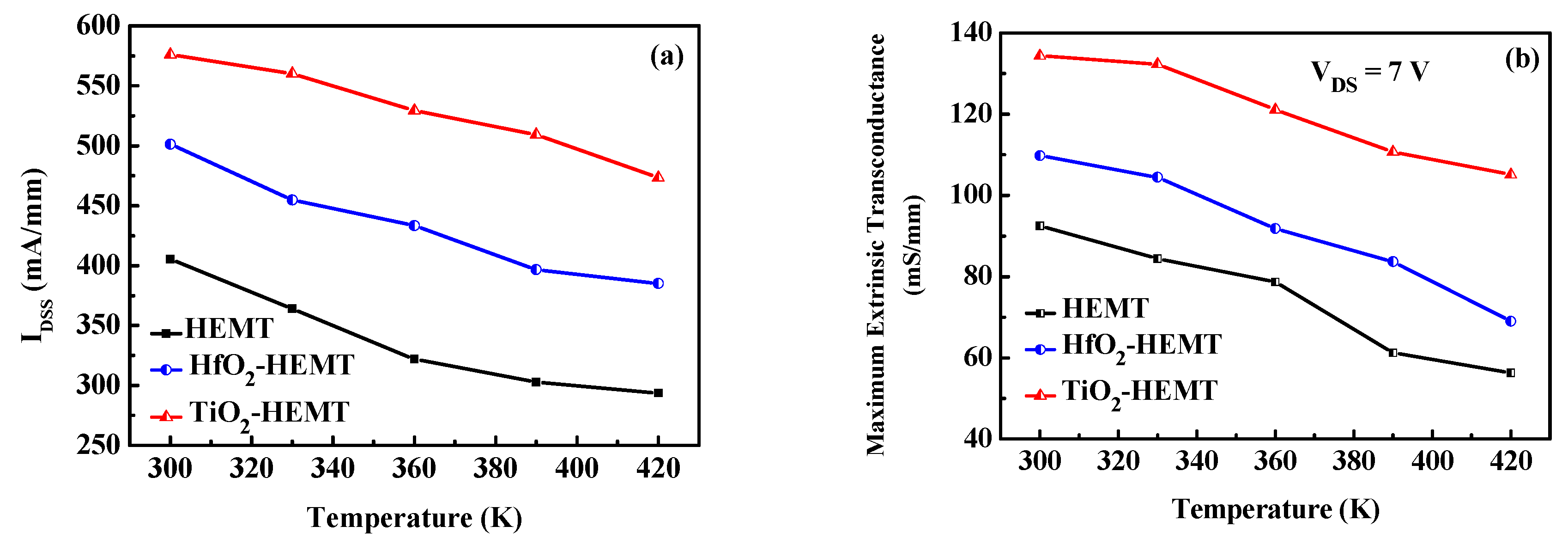
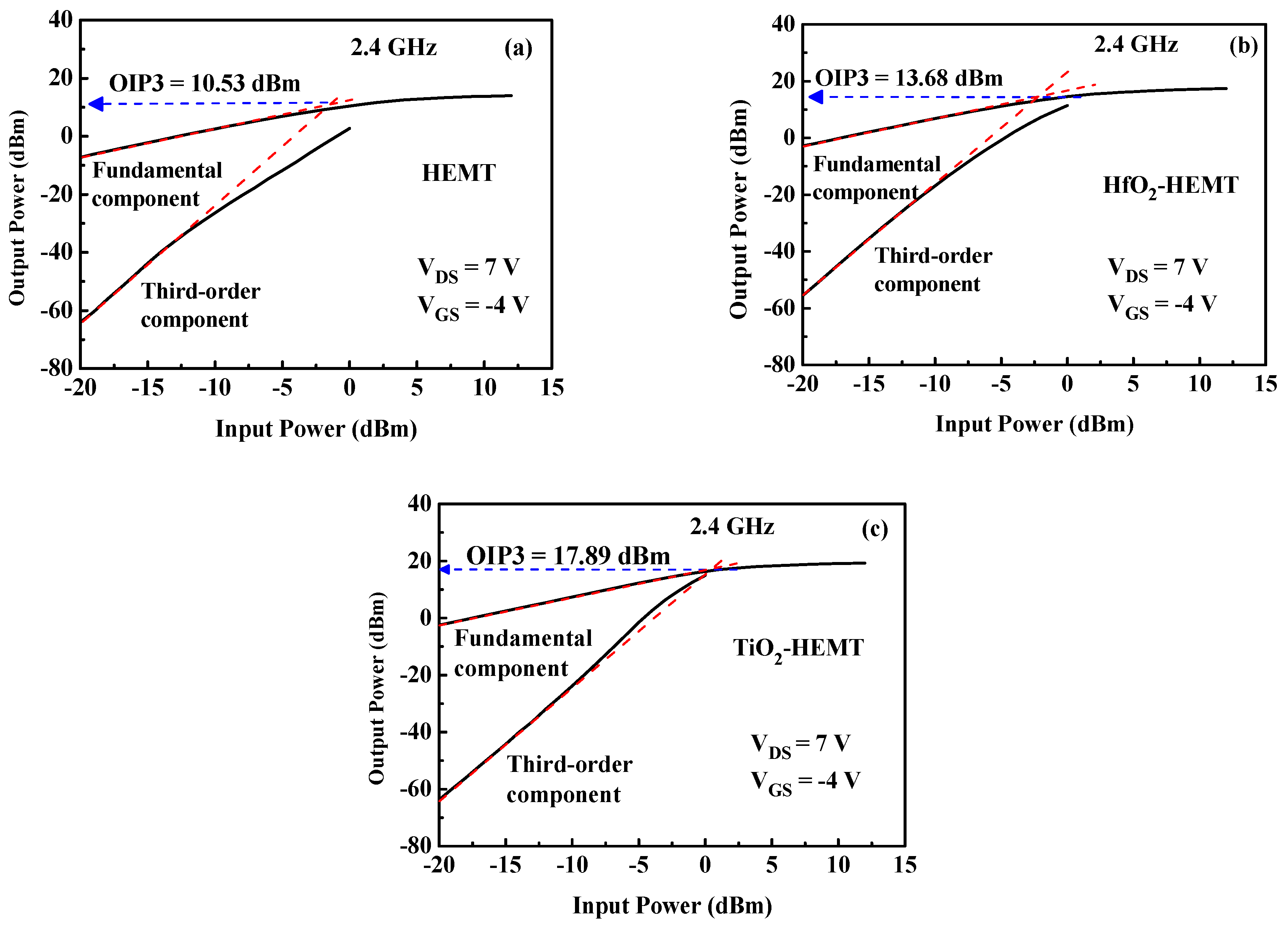
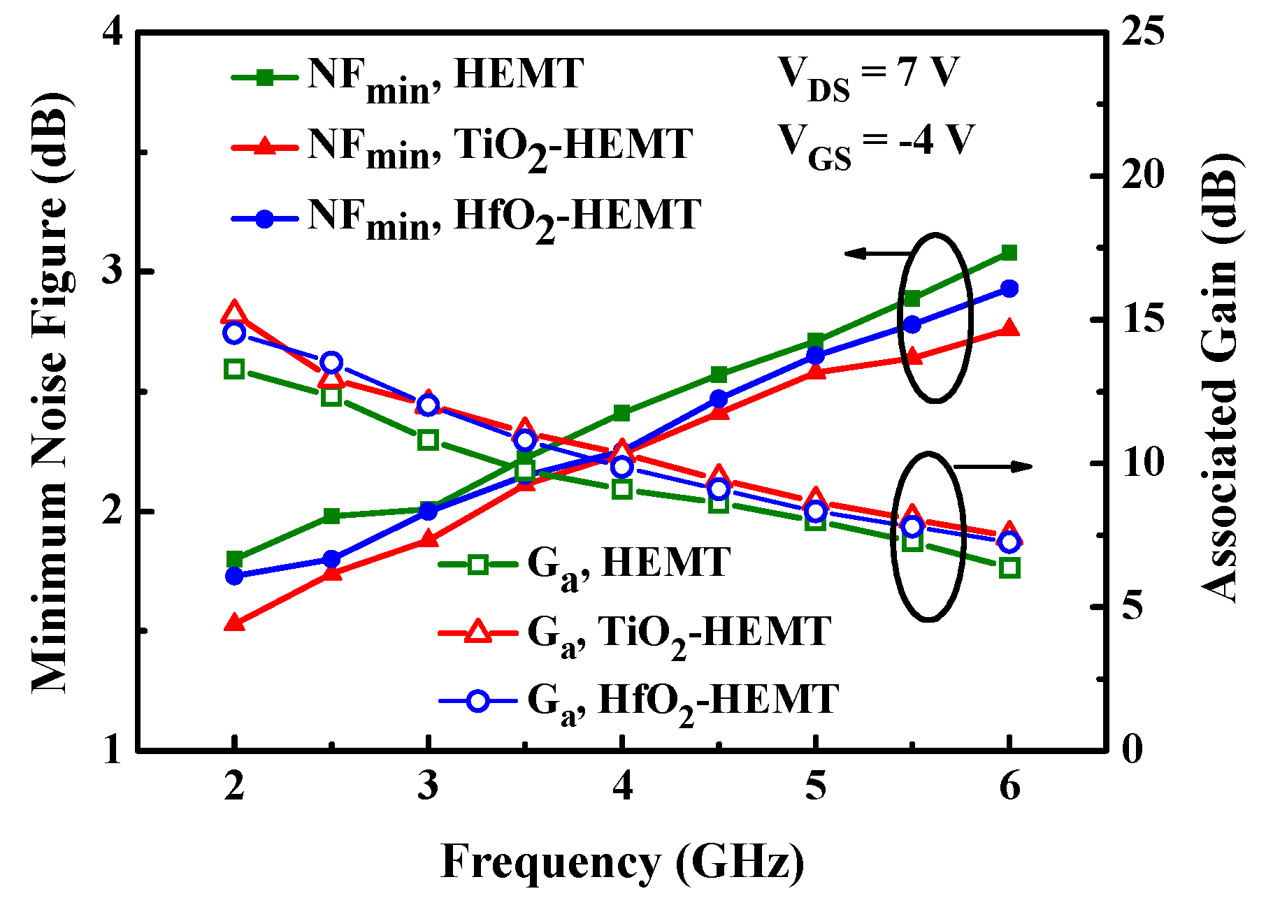
3. Results and Discussion

TEM samples are examined in a JEM-2100F (JEOL Co., Japan) operating at an accelerating voltage of 200 kV. Figure 2 illustrates the TEM cross section of the HEMTs with HfO2 and TiO2. The thicknesses of HfO2 and TiO2 films are approximately 22.65 and 19.79 nm, respectively.
The unpassivated and passivated HEMTs are subjected to high-temperature testing. Figure 3 presents the drain currents (IDS) at different temperatures versus drain-to-source voltage (VDS). The DC measurements are taken as functions of temperatures over the range 300 to 420 K. Figure 4 shows the extrinsic transconductance (gm) and drain current versus gate-to-source voltage of the studied HEMTs at various temperatures. The gate voltage swing (GVS) is defined by the voltage range within which the gm value deviates from its maximum value by 20%. The GVS value is increased from 1.7 V to 3.2 V at 300 K after TiO2 passivation. IDS versus VDS at pinch-off conditions and the threshold drain current characteristics at 300 K for the three HEMTs herein were studied [11]. Figure 5a plots drain current at VGS = 0 V (IDSS) versus temperature of the studied HEMTs. Experimental results reveal that IDSS values of the studied HEMTs are increased when the HEMTs are passivated. The increased drain current density is attributable to the increased sheet electron concentration after passivation [8,11]. The studied three HEMTs depicts good pinch-off characteristics at various temperatures. Increasing the temperature decreases IDSS. The falloff in drain current density at elevated temperatures result from the degradation of the electron mobility. Furthermore, the threshold voltage (Vth) is extracted by linear extrapolation of the root of drain current against Vg curves. The values of Vth of the TiO2-HEMT are −5.5, −5.33, −5.2, −4.96, and −4.89 V at 300, 330, 360, 390, and 420 K, respectively. The magnitude of the Vth value is reduced at high temperature because of the decreased drain current density.
Figure 5b plots the maximum extrinsic transconductance (gm,max) versus temperature of the investigated HEMTs. When the temperature is increased, the maximum extrinsic transconductance varies in the same tendency as IDSS. At 420 K, the gm,max values for HEMT, HfO2-HEMT, and TiO2-HEMT are 56.3, 69, and 105 mS/mm, respectively. Experimental results demonstrate the TiO2-HEMT perform well even at high temperatures.
Two-tone intermodulation distortion is measured to demonstrate the large-signal linearity performance. Figure 6 shows the fundamental and third-order output powers versus input power of the studied devices. The red dashed lines are extrapolated to predict the intersection at the third-order intercept point (OIP3). The values of OIP3 are 10.5, 13.7, and 17.9 dBm, respectively. HfO2 passivation increases the OIP3 value by around 30% and TiO2 passivation increases it by 70%. The large-signal linearity of the HEMT is significantly improved when the HEMT is passivated by TiO2. The improved device linearity of the TiO2-HEMT is attributed to increased gm,max [18] and GVS values [20].
Noise figure is measured over the 2–6 GHz frequency range using an ATN NP5B noise parameter test set in conjunction with the HP-8510C network analyzer. Figure 7 shows the minimum noise figure (NFmin) and associated power gain (Ga) versus frequency for the studied HEMTs. Figure 7 reveals that the relationship between the noise and frequency is near linear. Quantitatively, NFmin is given by [21,22,23]
N F min = 1 + 2 π f k C g s R s + R g g m
where f is frequency; k is the Fukui constant; Cgs is the input gate-source capacitance; Rs is the source series resistance, and Rg is the gate series resistance. The NFmin values of HEMT, HfO2-HEMT, and TiO2-HEMT are 1.94 dB, 1.79 dB, and 1.68 dB. The TiO2-HEMT has the smallest NFmin of the three devices because it has the highest gm. Furthermore, the associate gain of the TiO2-HEMT is also improved.

4. Conclusions

AlGaN/GaN/silicon grown by MOCVD have been successfully fabricated and measured. The high-temperature characteristics of the proposed devices are investigated. TiO2-HEMT exhibits the best large-signal linearity of the studied devices. Furthermore, the NFmin value of TiO2-HEMT is smallest of the studied devices herein.

Author Contributions

Investigation, Y.-S.L.; data curation, S.-F.L.; writing, Y.-S.L.; supervision, Y.-S.L. All authors have read and agreed to the published version of the manuscript.

Funding

This research was funded by the Ministry of Science and Technology, Taiwan, grant number MOST 108-2221-E-259-002-MY2.

Conflicts of Interest

The authors declare no conflict of interest.

References

  1. Wang, T.B.; Hsu, W.C.; Su, J.L.; Hsu, R.T.; Wu, Y.H.; Lin, Y.S.; Su, K.H. Comparison of Al0.32Ga0.68N/GaN Heterostructure Field-Effect Transistors with Different Channel Thicknesses. J. Electrochem. Soc. 2007, 154, H131–H133. [Google Scholar] [CrossRef]
  2. Hung, C.W.; Chang, C.H.; Chen, W.C.; Chen, C.C.; Chen, H.I.; Tsai, Y.T.; Tsai, J.H.; Liu, W.C. A Pt/AlGaN/GaN Heterostructure Field-Effect Transistor (HFET) Prepared by an Electrophoretic Deposition (EPD)-Gate Approach. Solid-State Electron. 2016, 124, 5–9. [Google Scholar] [CrossRef]
  3. Wojtasiak, W.; Góralczyk, M.; Gryglewski, D.; Zając, M.; Kucharski, R.; Prystawko, P.; Piotrowska, A.; Ekielski, M.; Kamińska, E.; Taube, A.; et al. AlGaN/GaN High Electron Mobility Transistors on Semi-Insulating Ammono-GaN Substrates with Regrown Ohmic Contacts. Micromachines 2018, 9, 546. [Google Scholar] [CrossRef] [PubMed] [Green Version]
  4. Abid, I.; Kabouche, R.; Bougerol, C.; Pernot, J.; Masante, C.; Comyn, R.; Cordier, Y.; Medjdoub, F. High Lateral Breakdown Voltage in Thin Channel, AlGaN/GaN High Electron Mobility Transistors on AlN/Sapphire Templates. Micromachines 2019, 10, 690. [Google Scholar] [CrossRef] [Green Version]
  5. Lin, Y.C.; Chen, S.H.; Lee, P.H.; Lai, K.H.; Huang, T.J.; Chang, E.Y.; Hsu, H.T. Gallium Nitride (GaN) High-Electron-Mobility Transistors with Thick Copper Metallization Featuring a Power Density of 8.2 W/mm for Ka-Band Applications. Micromachines 2020, 11, 222. [Google Scholar] [CrossRef] [Green Version]
  6. Lin, Y.S.; Chen, B.Y. Effects of Surface Passivation and Temperature on AlGaAs/InGaAs High-Electron Mobility Transistor. Microelectron. Eng. 2019, 214, 100–103. [Google Scholar] [CrossRef]
  7. Han, D.; Ruiz, D.C.; Bonomo, G.; Saranovac, T.; Ostinelli, O.J.S.; Bolognesi, C.R. Low-Noise Microwave Performance of 30 nm GaInAs MOS-HEMTs: Comparison to Low-Noise HEMTs. IEEE Electron Device Lett. 2020, 41, 1320–1323. [Google Scholar] [CrossRef]
  8. Liu, C.; Chor, E.F.; Tan, L.S. Enhanced device performance of AlGaN/GaN HEMTs Using HfO2 High-k Dielectric for Surface Passivation and Gate Oxide. Semicond. Sci. Tech. 2007, 22, 522–527. [Google Scholar] [CrossRef]
  9. Fitch, R.C.; Walker, D.E., Jr.; Chabak, K.D.; Gillespie, J.K.; Kossler, M.; Trejo, M.; Crespo, A.; Liu, L.; Kang, T.S.; Lo, C.-F.; et al. Comparison of Passivation Layers for AlGaN/GaN High Electron Mobility Transistors. J. Vac. Sci. Technol. B 2011, 29, 061204. [Google Scholar] [CrossRef]
  10. Fehlberg, T.B.; Milne, J.S.; Umana-Membreno, G.A.; Keller, S.; Mishra, U.K.; Nener, B.D.; Parish, G. Transport Studies of AlGaN/GaN Heterostructures of Different Al Mole Fractions with Variable SiNx Passivation Stress. IEEE Trans. Electron Devices 2011, 58, 2589. [Google Scholar] [CrossRef]
  11. Lin, Y.S.; Lin, S.F.; Hsu, W.C. Microwave and power characteristics of AlGaN/GaN/Si High-Electron Mobility Transistors with HfO2 and TiO2 Passivation. Semicond. Sci. Technol. 2015, 30, 015016. [Google Scholar] [CrossRef]
  12. Geng, K.; Chen, D.; Zhou, Q.; Wang, H. AlGaN/GaN MIS-HEMT with PECVD SiNx, SiON, SiO2 as Gate Dielectric and Passivation Layer. Electronics 2018, 7, 416. [Google Scholar] [CrossRef] [Green Version]
  13. Lin, Y.S.; Goa, W.H. High-temperature Stability of Improved AlGaN/AlN/GaN HEMT with Pre-Gate Metal Treatment. IEICE Electron. Express 2019, 16, 1–8. [Google Scholar] [CrossRef]
  14. Gao, S.; Zhou, Q.; Liu, X.; Wang, H. Breakdown Enhancement and Current Collapse Suppression in AlGaN/GaN HEMT by NiOx/SiNx and Al2O3/SiNx as Gate Dielectric Layer and Passivation layer. IEEE Electron Device Lett. 2019, 40, 1921–1924. [Google Scholar] [CrossRef]
  15. Cheng, K.Y.; Wu, S.C.; Yu, C.J.; Wang, T.W.; Liao, J.H.; Wu, M.C. Comparative Study on Performance of AlGaN/GaN MS-HEMTs with SiNx, SiOx, and SiNO Surface Passivation. Solid-State Electron. 2020, 170, 107824. [Google Scholar] [CrossRef]
  16. Kang, M.J.; Kim, H.S.; Cha, H.Y.; Seo, K.S. Development of Catalytic-CVD SiNx Passivation Process for AlGaN/GaN-on-Si HEMTs. Crystals 2020, 10, 842. [Google Scholar] [CrossRef]
  17. Murugapandiyan, P.; Mohanbabu, A.; Lakshmi, V.R.; Ramakrishnan, V.N.; Varghese, A.; Wasim, M.O.H.D.; Baskaran, S.; Kumar, R.S.; Janakiraman, V. Performance Analysis of HfO2/InAlN/AlN/GaN HEMT with AlN Buffer Layer for High Power Microwave Applications. J. Sci. 2020, 5, 192–198. [Google Scholar] [CrossRef]
  18. Shrestha, P.; Guidry, M.; Romanczyk, B.; Hatui, N.; Wurm, C.; Krishna, A.; Pasayat, S.S.; Karnaty, R.R.; Keller, S.; Buckwalter, J.F.; et al. High Linearity and High Gain Performance of N-Polar GaN MIS-HEMT at 30 GHz. IEEE Electron Device Lett. 2020, 41, 681–684. [Google Scholar] [CrossRef]
  19. Li, S.; Liu, S.; Tian, Y.; Zhang, C.; Wei, J.; Tao, X.; Li, N.; Zhang, L.; Sun, W. High-Temperature Electrical Performances and Physics-Based Analysis of p-GaN HEMT Device. IET Power Electron. 2020, 13, 420–425. [Google Scholar] [CrossRef]
  20. Mi, M.; Wu, S.; Zhang, M.; Yang, L.; Hou, B.; Zhao, Z.; Guo, L.; Zhang, X.; Ma, X.; Hao, Y. Improving the Transconductance Flatness of InAlN/GaN HEMT by Modulating VT along the Gate Width. Appl. Phys. Express 2019, 12, 114001. [Google Scholar] [CrossRef]
  21. Fukui, H. Optimal Noise Figure of Microwave GaAs MESFET’s. IEEE Trans. Electron Devices 1979, 26, 1032–1037. [Google Scholar] [CrossRef]
  22. Fukui, H. Design of microwave GaAs MESFET’S for Broad-Band Low-Noise Amplifiers. IEEE Trans. Microw. Theory Tech. 1979, 27, 643–650. [Google Scholar] [CrossRef] [Green Version]
  23. Delagebeaudeuf, D.; Chevrier, J.; Laviron, M.; Delescluse, P. A New Relationship between the Fukui Coefficient and Optimal Current Value for Low-Noise Operation of Field-Effect Transistors. IEEE Electron Device Lett. 1985, 6, 444–445. [Google Scholar] [CrossRef]
Figure 1. Cross section of the studied passivated AlGaN/GaN high-electron mobility transistor (HEMT).
Micromachines 12 00007 g001
Figure 2. Cross-sectional TEM images of (a) HfO2-HEMT and (b) TiO2-HEMT.
Micromachines 12 00007 g002
Figure 3. Family of drain-source output curves of (a) HEMT, (b) HfO2-HEMT, and (c) TiO2-HEMT at various temperatures.
Micromachines 12 00007 g003aMicromachines 12 00007 g003b
Figure 4. Extrinsic transconductance and drain current characteristics of (a) HEMT, (b) HfO2-HEMT, and (c) TiO2-HEMT at various temperatures.
Micromachines 12 00007 g004
Figure 5. (a) IDSS and (b) gm,max of the studied HEMTs at various temperatures.
Micromachines 12 00007 g005
Figure 6. Fundamental output power and third-order intermodulation component of (a) HEMT, (b) HfO2-HEMT, and (c) TiO2-HEMT.
Micromachines 12 00007 g006
Figure 7. Minimum noise figure and associated gain of the studied (a) HEMT, (b) HfO2-HEMT, and TiO2-HEMT.
Micromachines 12 00007 g007
Publisher’s Note: MDPI stays neutral with regard to jurisdictional claims in published maps and institutional affiliations.

