Applying Foil Queue Microelectrode with Tapered Structure in Micro-EDM to Eliminate the Step Effect on the 3D Microstructure’s Surface

Abstract
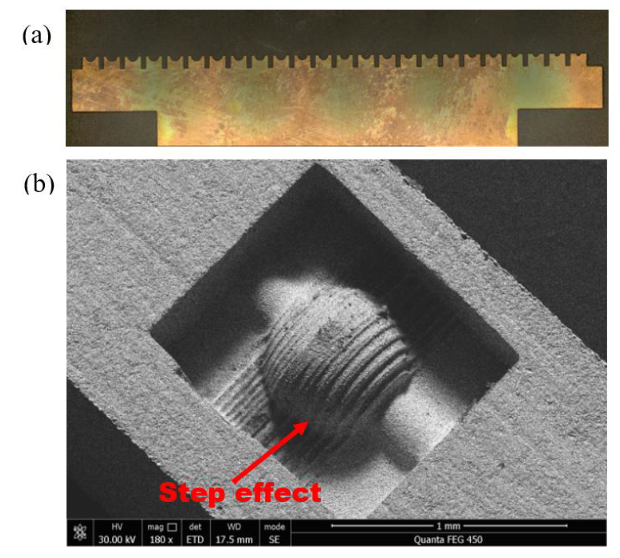
:1. Introduction
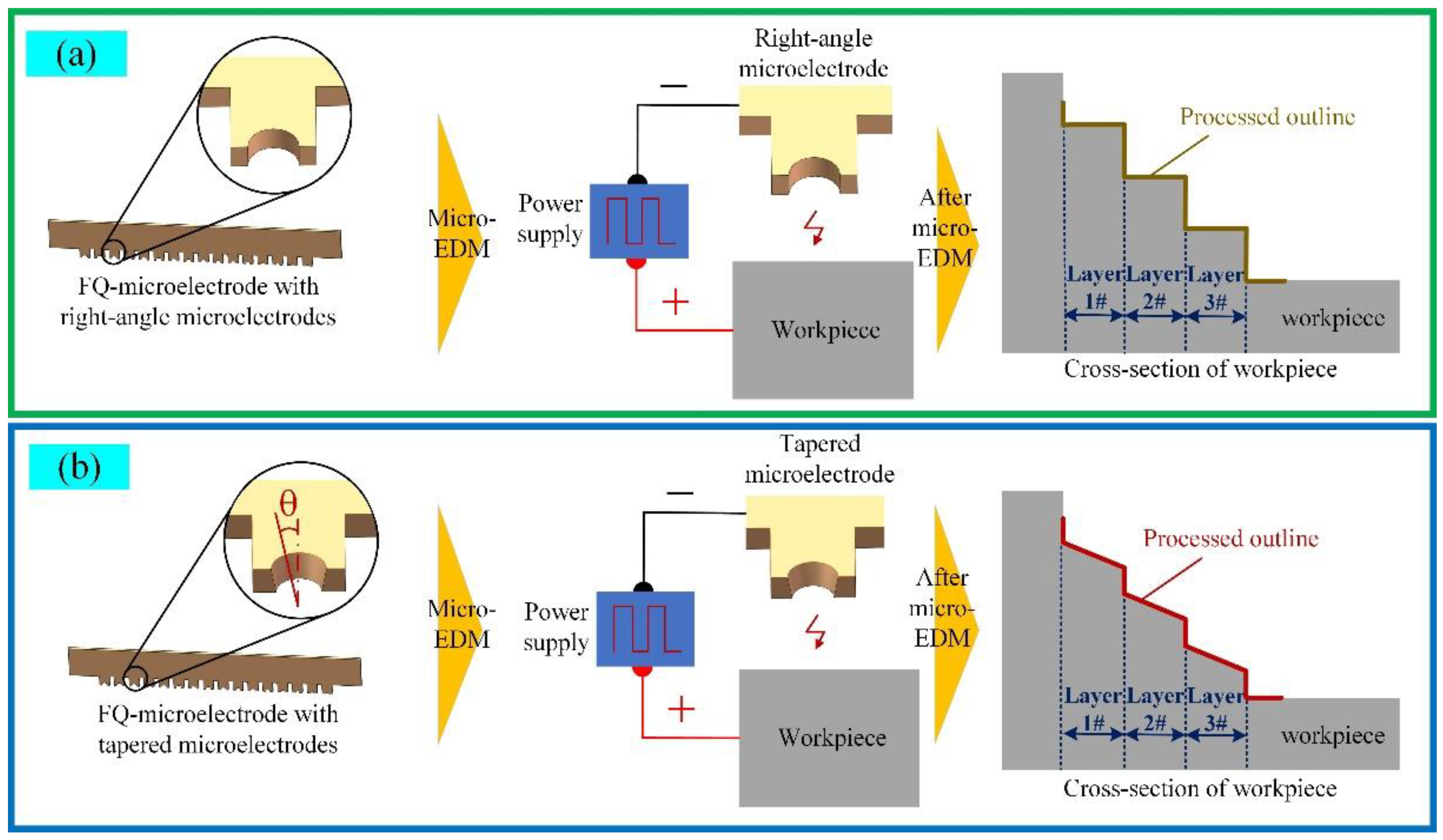
2. Method
3. Experimental Materials and Equipment
4. Experimental Results and Discussion
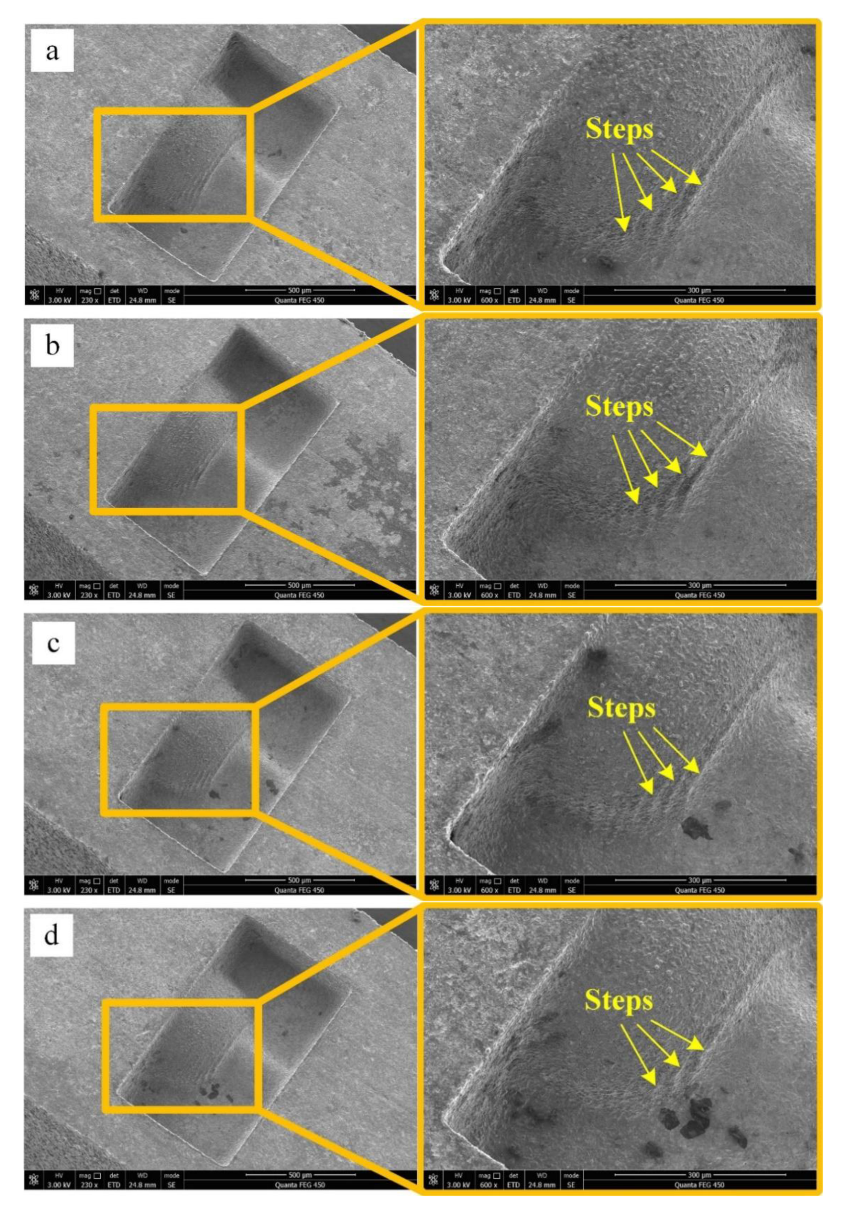
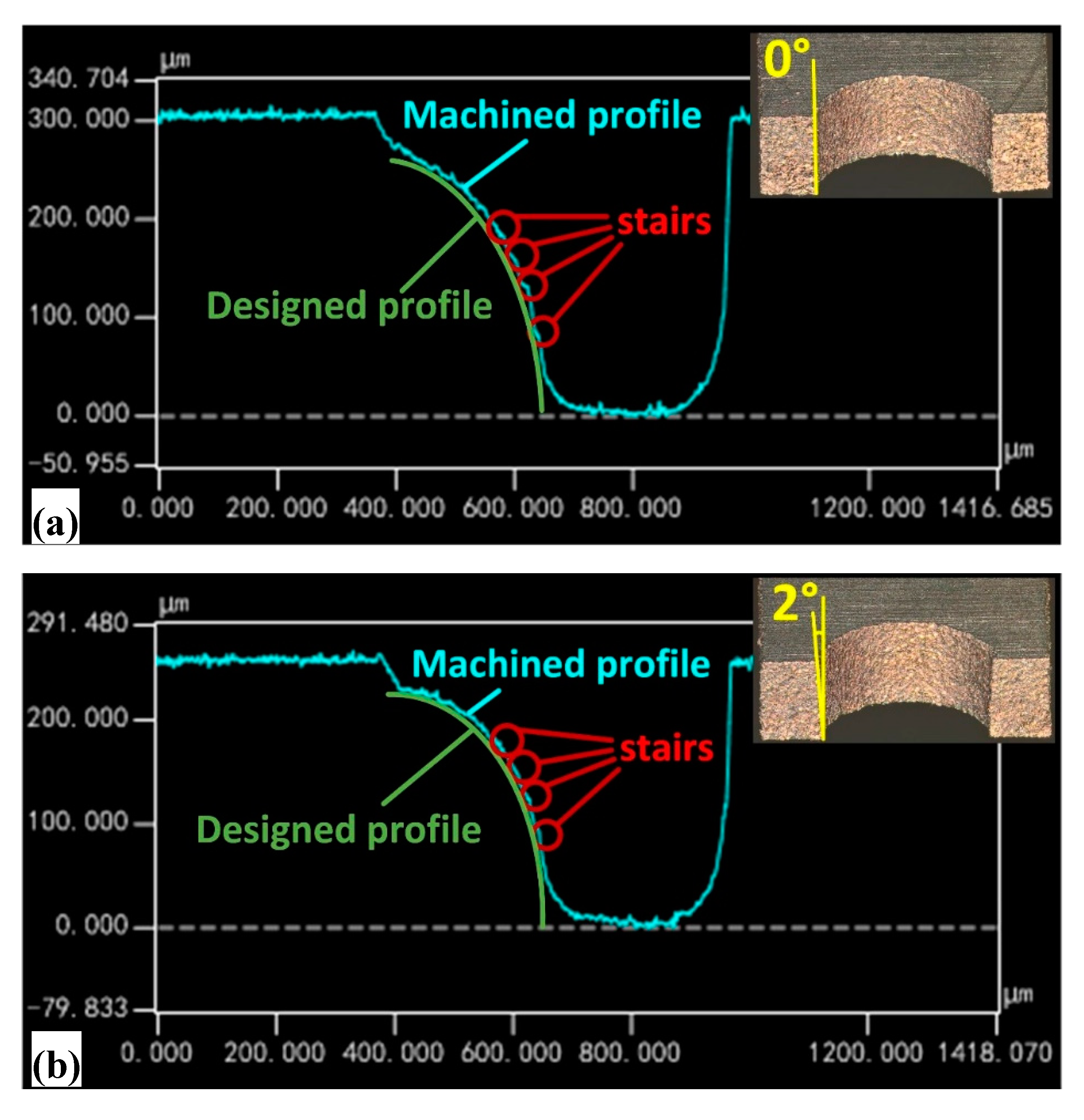
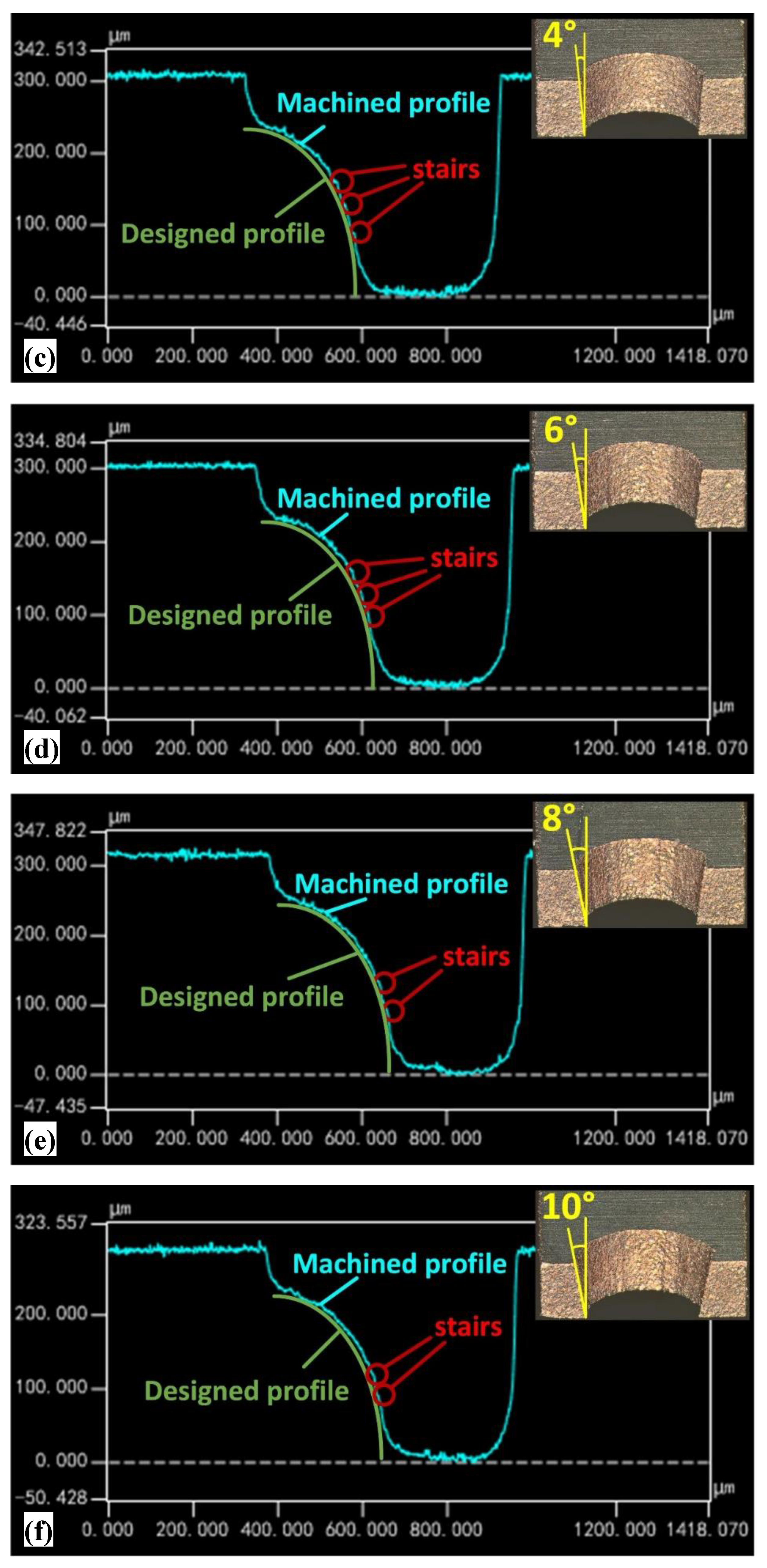
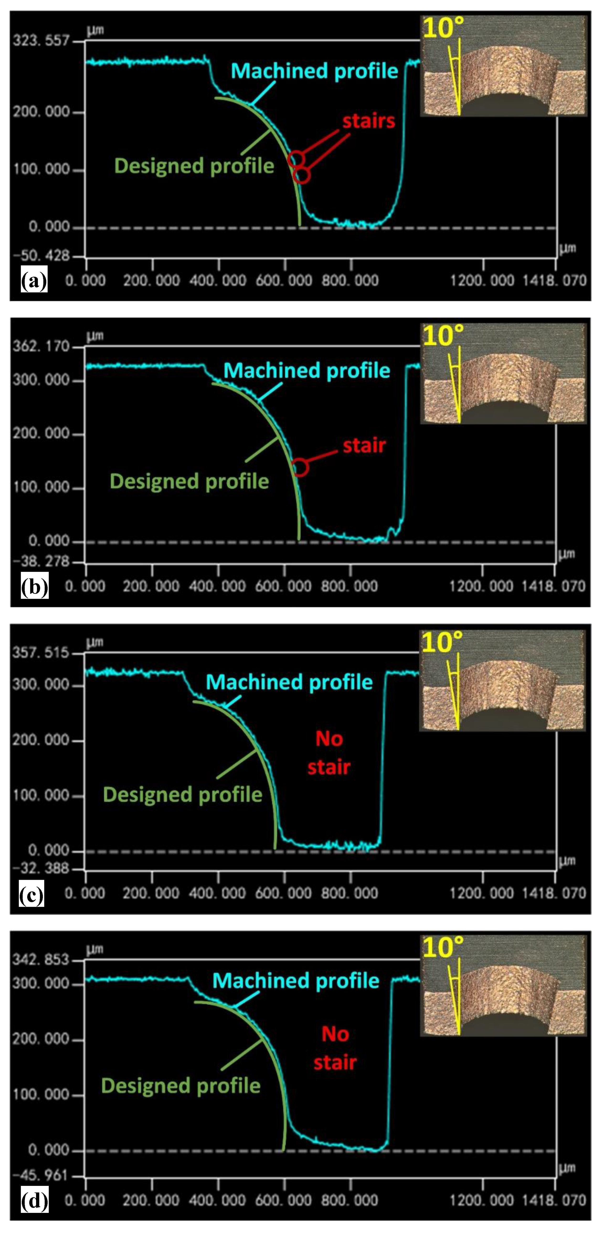
4.1. Influence of Taper Angle on the Elimination of Step Effect
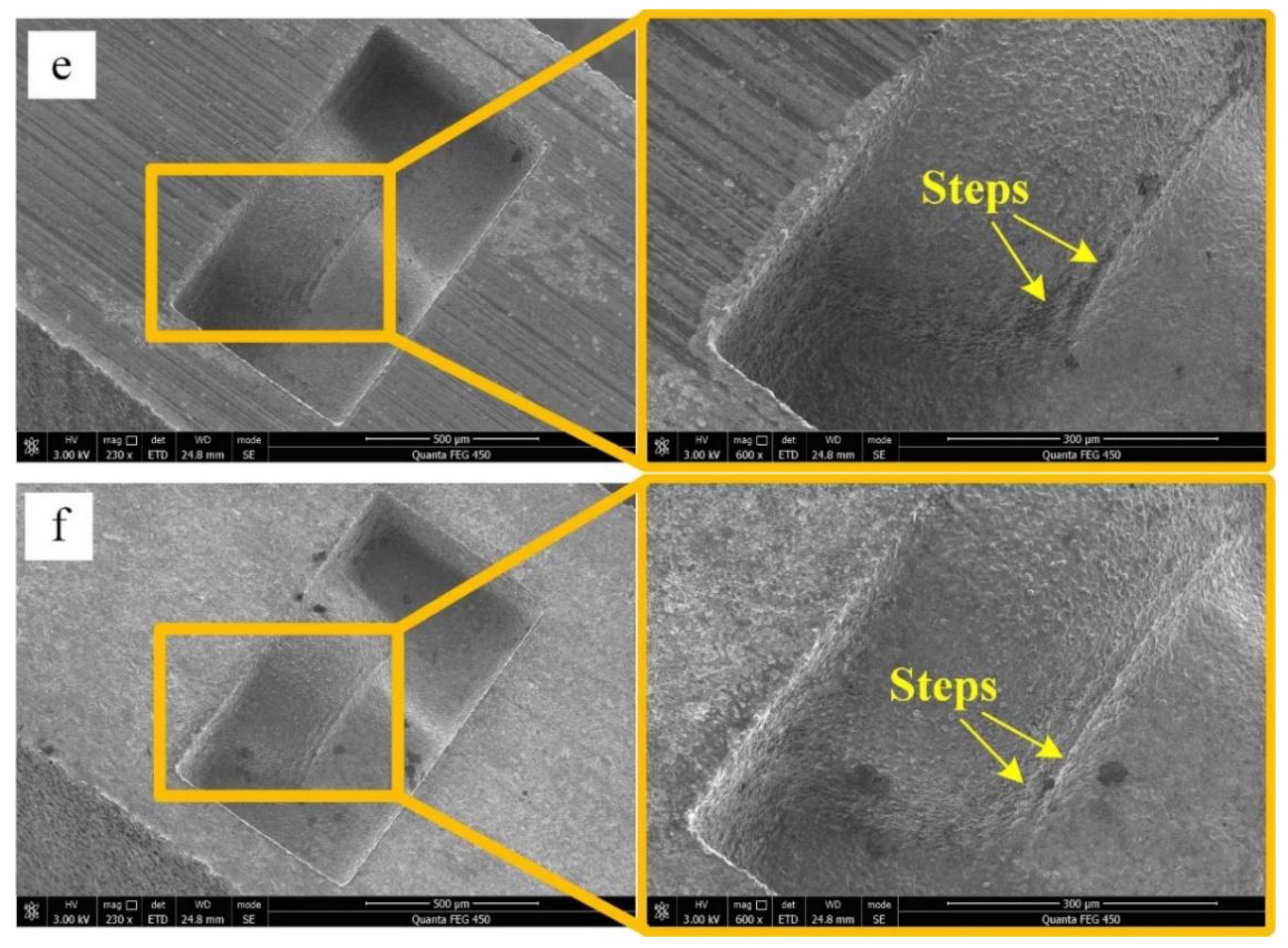
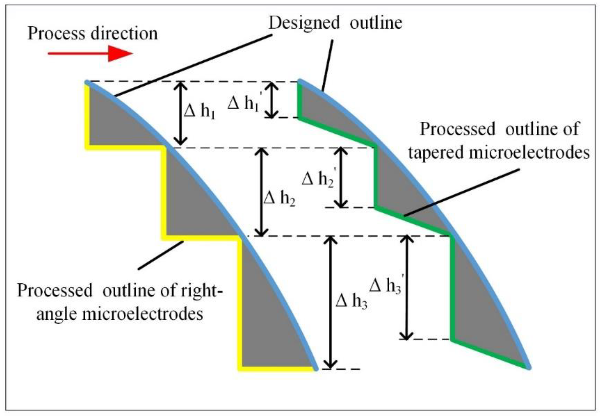
4.2. Influence of Numbers of F-Microelectrode on the Elimination of Step Effect
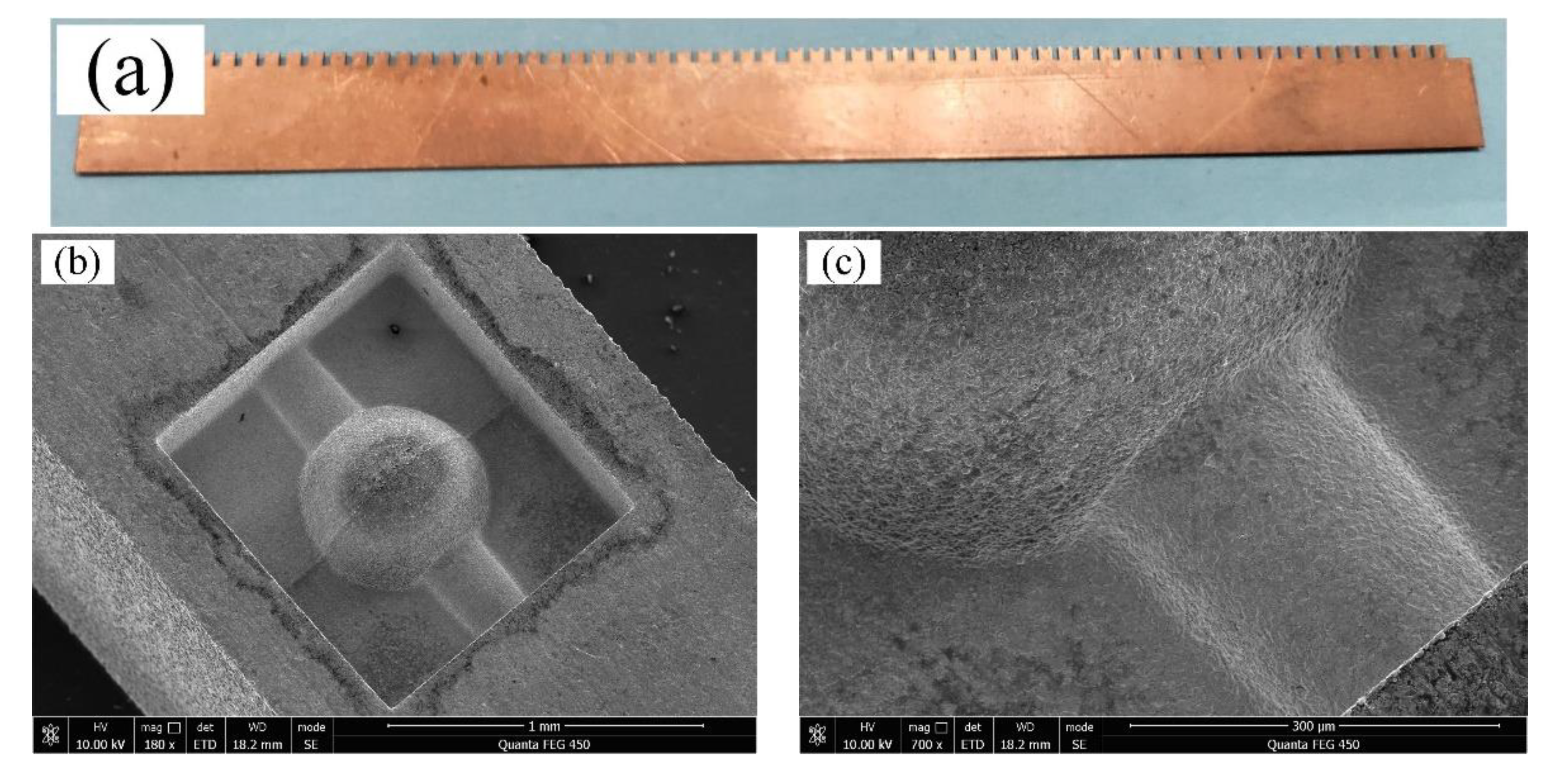
5. Application of FQ-Microelectrode with Tapered Structures in Micro-EDM
6. Conclusions
- (1)
- When the FQ-microelectrodes with tapered structures were used for micro-EDM, the step effect on the surface of the 3D microstructure can be significantly weakened and the shape accuracy can be improved.
- (2)
- By reducing the slice thickness of the 3D microelectrode model and thereby increasing the number of F-microelectrodes, the step effect on the 3D microstructure surface can be further eliminated. When the taper angle of the F-microelectrode is 10° and the number of F-microelectrodes is 40, the step effect on the surface of the 3D microstructure can be essentially eliminated.
- (3)
- Under the processing voltage of 120 V, pulse width of 1 μs and pulse interval of 10 μs, the FQ-microelectrode (including 40 F-microelectrodes) with 10° taper angle was used for micro-EDM. The obtained 3D microstructure has good surface quality and the step effect was essentially eliminated. The dimensional accuracy of 3D microstructure is well and the maximum dimensional error is within 10 μm.
Author Contributions
Funding
Acknowledgments
Conflicts of Interest
References
- Hourmand, M.; Sarhan, A.A.D.; Sayuti, M. Micro-electrode fabrication processes for micro-EDM drilling and milling: A state-of-the-art review. Int. J. Adv. Manuf. Technol. 2017, 91, 1023–1056. [Google Scholar] [CrossRef]
- Bilal, A.; Pervej Jahan, M.; Talamona, D.; Perveen, A. Electro-Discharge Machining of Ceramics: A Review. Micromachines 2019, 10, 10. [Google Scholar] [CrossRef] [PubMed] [Green Version]
- Yu, Z.Y.; Masuzawa, T.; Fujino, M. Micro-EDM for Three-Dimensional Cavities-Development of Uniform Wear Method. CIRP Ann. 1998, 47, 169–172. [Google Scholar] [CrossRef]
- Rajurkar, K.P.; Yu, Z.Y. 3D Micro-EDM Using CAD/CAM. CIRP Ann. 2000, 49, 127–130. [Google Scholar] [CrossRef]
- Yang, F.; Qian, J.; Wang, J.; Reynaerts, D. Simulation and experimental analysis of alternating-current phenomenon in micro-EDM with a RC-type generator. J. Mater. Process. Technol. 2018, 255, 865–875. [Google Scholar] [CrossRef]
- Tong, H.; Li, Y.; Wang, Y.; Yu, D. Servo scanning 3D micro-EDM based on macro/micro-dual-feed spindle. Int. J. Mach. Tools Manuf. 2008, 48, 858–869. [Google Scholar] [CrossRef]
- Fu, X.Z.; Zhang, Q.H.; Gao, L.Y.; Liu, Q.Y.; Wang, K.; Zhang, Y.W. A novel micro-EDM-piezoelectric self-adaptive micro-EDM. Int. J. Adv. Manuf. Technol. 2016, 85, 817–824. [Google Scholar] [CrossRef]
- Wang, J.; Yang, F.; Qian, J.; Reynaerts, D. Study of alternating current flow in micro-EDM through real-time pulse counting. J. Mater. Process. Technol. 2016, 231, 179–188. [Google Scholar] [CrossRef]
- Wu, W.; Wu, X.Y.; Lei, J.G.; Xu, B.; Jiang, K.; Wu, Z.Z.; Yin, H.M.; Li, W. Fabrication of deep-narrow microgrooves by micro-EDM using rotary dentate disc foil electrodes in emulsion. J. Micromech. Microeng. 2019, 29, 035014. [Google Scholar] [CrossRef]
- Schulze, V.; Weber, P.; Ruhs, C. Increase of process reliability in the micro-machining processes EDM-milling and laser ablation using on-machine sensors. J. Mater. Process. Technol. 2012, 212, 625–632. [Google Scholar] [CrossRef]
- Wang, Y.K.; Chen, X.; Wang, Z.L.; Li, H.C.; Liu, H.Z. Fabrication of micro-rotating structure by micro reciprocated wire-EDM. J. Micromech. Microeng. 2016, 26, 115014. [Google Scholar] [CrossRef]
- Sun, Y.; Gong, Y.D. Experimental study on the microelectrodes fabrication using low speed wire electrical discharge turning (LS-WEDT) combined with multiple cutting strategy. J. Mater. Process. Technol. 2017, 250, 121–131. [Google Scholar] [CrossRef]
- Liu, Q.; Zhang, Q.; Zhang, M.; Yang, F. Study on the Discharge Characteristics of Single-Pulse Discharge in Micro-EDM. Micromachines 2020, 11, 55. [Google Scholar] [CrossRef] [PubMed] [Green Version]
- Bellotti, M.; Qian, J.; Reynaerts, D. Process Fingerprint in Micro-EDM Drilling. Micromachines 2019, 10, 240. [Google Scholar] [CrossRef] [Green Version]
- D’Urso, G.; Giardini, C.; Quarto, M.; Maccarini, G. Cost Index Model for the Process Performance Optimization of Micro-EDM Drilling on Tungsten Carbide. Micromachines 2017, 8, 251. [Google Scholar] [CrossRef] [Green Version]
- Wyszynski, D.; Bizon, W.; Miernik, K. Electrodischarge Drilling of Microholes in c-BN. Micromachines 2020, 11, 179. [Google Scholar] [CrossRef] [Green Version]
- Ahmed, N.; Pervez Mughal, M.; Shoaib, W.; Raza, S.F.; Alahmari, A.M. WEDM of Copper for the Fabrication of Large Surface-Area Micro-Channels: A Prerequisite for the High Heat-Transfer Rate. Micromachines 2020, 11, 173. [Google Scholar] [CrossRef] [Green Version]
- Świercz, R.; Oniszczuk-Świercz, D.; Chmielewski, T. Multi-Response Optimization of Electrical Discharge Machining Using the Desirability Function. Micromachines 2019, 10, 72. [Google Scholar] [CrossRef] [Green Version]
- Liu, Y.; Chang, H.; Zhang, W.C.; Ma, F.J.; Sha, Z.H.; Zhang, S.F. A Simulation Study of Debris Removal Process in Ultrasonic Vibration Assisted Electrical Discharge Machining (EDM) of Deep Holes. Micromachines 2018, 9, 378. [Google Scholar] [CrossRef] [Green Version]
- Almacinha, J.A.; Lopes, A.M.; Rosa, P.; Marafona, J.D. How Hydrogen Dielectric Strength Forces the Work Voltage in the Electric Discharge Machining. Micromachines 2018, 9, 240. [Google Scholar] [CrossRef] [Green Version]
- Wang, Y.K.; Wang, H.; Zhang, Y.X.; He, X.L.; Wang, Z.L.; Chi, G.X.; Chen, X.; Song, M.S. Micro Electrochemical Machining of Array Micro-Grooves Using In-Situ Disk Electrode Fabricated by Micro-WEDM. Micromachines 2020, 11, 66. [Google Scholar] [CrossRef] [PubMed] [Green Version]
- Zhang, Y.; Wang, C.; Wang, Y.; Ji, L.; Tang, J.; Ni, Q. Effects of Helical Tube Electrode Structure on Mixed Machining Product Transfer in Micro-Machining Channel during Tube Electrode High-Speed Electrochemical Discharge Machining. Micromachines 2019, 10, 634. [Google Scholar] [CrossRef] [Green Version]
- Wang, F.; Zhang, Y.; Liu, G.; Wang, Q. Improvement of processing quality based on VHF resonant micro-EDM pulse generator. Int. J. Adv. Manuf. Technol. 2019, 104, 3663–3677. [Google Scholar] [CrossRef]
- Yu, Z.; Li, D.; Yang, J.; Zeng, Z.; Yang, X.; Li, J. Fabrication of micro punching mold for micro complex shape part by micro EDM. Int. J. Adv. Manuf. Technol. 2019, 100, 743–749. [Google Scholar] [CrossRef]
- Huang, C.H.; Yang, A.B.; Hsu, C.Y. The optimization of micro EDM milling of Ti–6Al–4V using a grey Taguchi method and its improvement by electrode coating. Int. J. Adv. Manuf. Technol. 2018, 96, 3851–3859. [Google Scholar] [CrossRef]
- Beigmoradi, S.; Ghoreishi, M.; Vahdati, M. Optimum design of vibratory electrode in micro-EDM process. Int. J. Adv. Manuf. Technol. 2018, 95, 3731–3744. [Google Scholar] [CrossRef]
- Xu, B.; Wu, X.Y.; Lei, J.G.; Cheng, R.; Ruan, S.C.; Wang, Z.L. Laminated fabrication of 3D micro-electrode based on WEDM and thermal diffusion welding. J. Mater. Process. Technol. 2015, 221, 56–65. [Google Scholar] [CrossRef]
- Xu, B.; Wu, X.Y.; Ma, J.; Liang, X.; Lei, J.G.; Wu, B.; Ruan, S.C.; Wang, Z.L. Micro-electrical discharge machining of 3D micro-molds from Pd40Cu30P20Ni10 metallic glass by using laminated 3D micro-electrodes. J. Micromech. Microeng. 2016, 26, 035004. [Google Scholar] [CrossRef]
- Xu, B.; Guo, K.; Wu, X.Y.; Lei, J.G.; Liang, X.; Guo, D.J.; Ma, J.; Cheng, R. Applying a foil queue micro-electrode in micro-EDM to fabricate a 3D micro-structure. J. Micromech. Microeng. 2018, 28, 055008. [Google Scholar] [CrossRef]
- Xu, B.; Guo, K.; Zhu, L.K.; Wu, X.Y.; Lei, J.G.; Zhao, H.; Tang, Y.; Liang, X. The wear of foil queue microelectrode in 3D micro-EDM. Int. J. Adv. Manuf. Technol. 2019, 104, 3107–3117. [Google Scholar] [CrossRef]


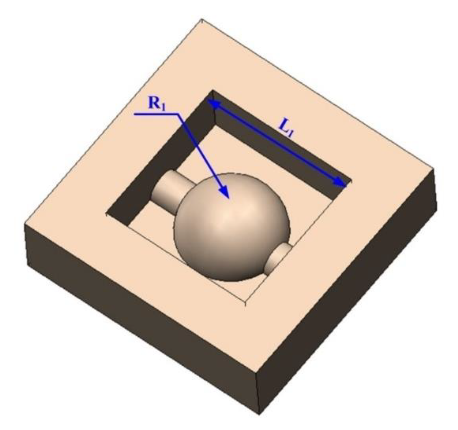
| Dimensional Symbols | Dimensional Values (μm) | Processing Time | ||
|---|---|---|---|---|
| CAD Model Shown in Figure 9 | Micro-EDM Result Shown in Figure 8 | Errors | ||
| L1 | 1156 | 1150 | 6 | 120 min |
| R1 | 300 | 295 | 5 | |
| Depth | 330 | 322 | 8 | |
© 2020 by the authors. Licensee MDPI, Basel, Switzerland. This article is an open access article distributed under the terms and conditions of the Creative Commons Attribution (CC BY) license (http://creativecommons.org/licenses/by/4.0/).
Share and Cite
Xu, B.; Guo, K.; Zhu, L.; Wu, X.; Lei, J. Applying Foil Queue Microelectrode with Tapered Structure in Micro-EDM to Eliminate the Step Effect on the 3D Microstructure’s Surface. Micromachines 2020, 11, 335. https://doi.org/10.3390/mi11030335
Xu B, Guo K, Zhu L, Wu X, Lei J. Applying Foil Queue Microelectrode with Tapered Structure in Micro-EDM to Eliminate the Step Effect on the 3D Microstructure’s Surface. Micromachines. 2020; 11(3):335. https://doi.org/10.3390/mi11030335
Chicago/Turabian StyleXu, Bin, Kang Guo, Likuan Zhu, Xiaoyu Wu, and Jianguo Lei. 2020. "Applying Foil Queue Microelectrode with Tapered Structure in Micro-EDM to Eliminate the Step Effect on the 3D Microstructure’s Surface" Micromachines 11, no. 3: 335. https://doi.org/10.3390/mi11030335