Optically Transparent Metasurface Absorber Based on Reconfigurable and Flexible Indium Tin Oxide Film

Abstract
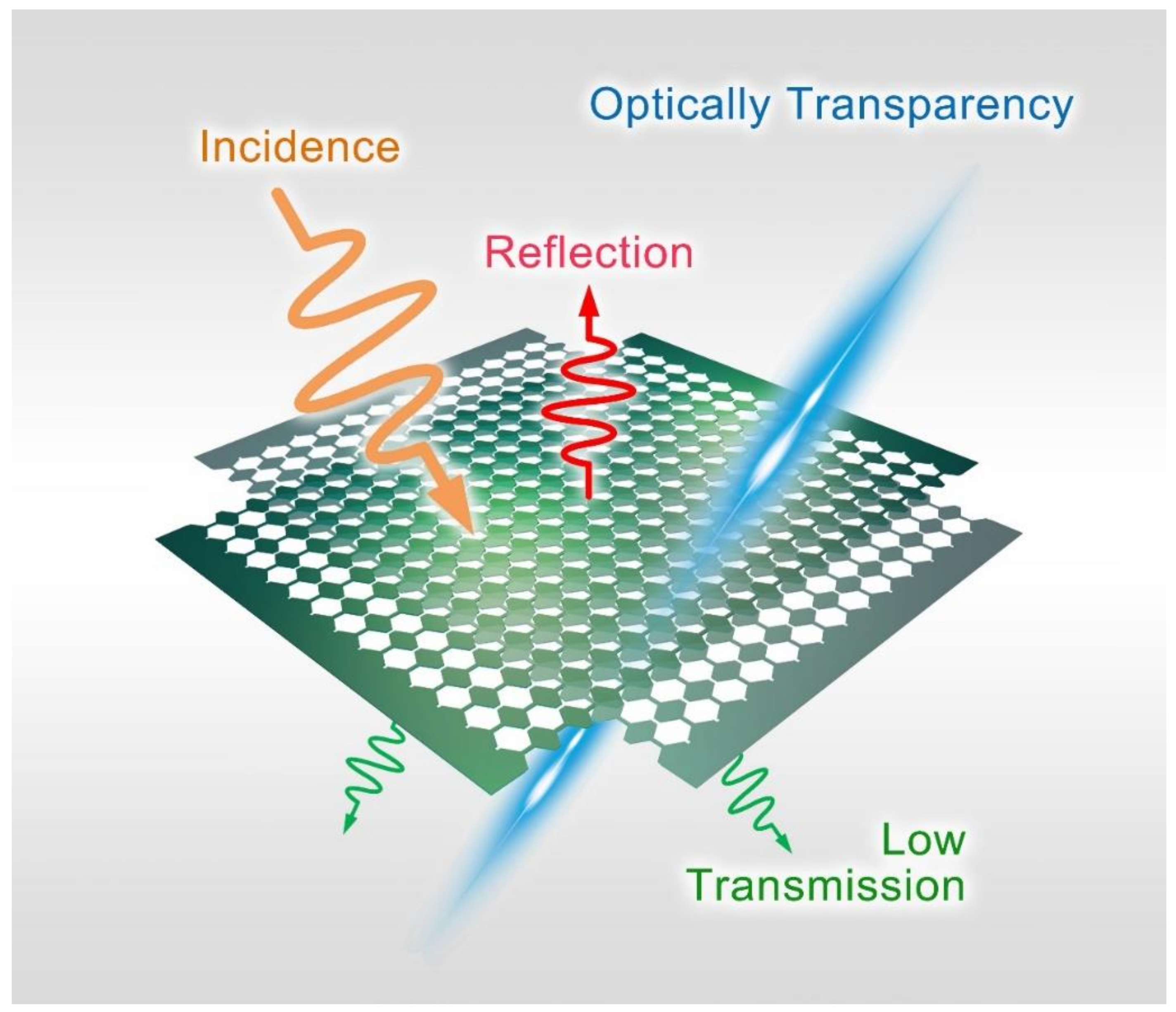
:1. Introduction
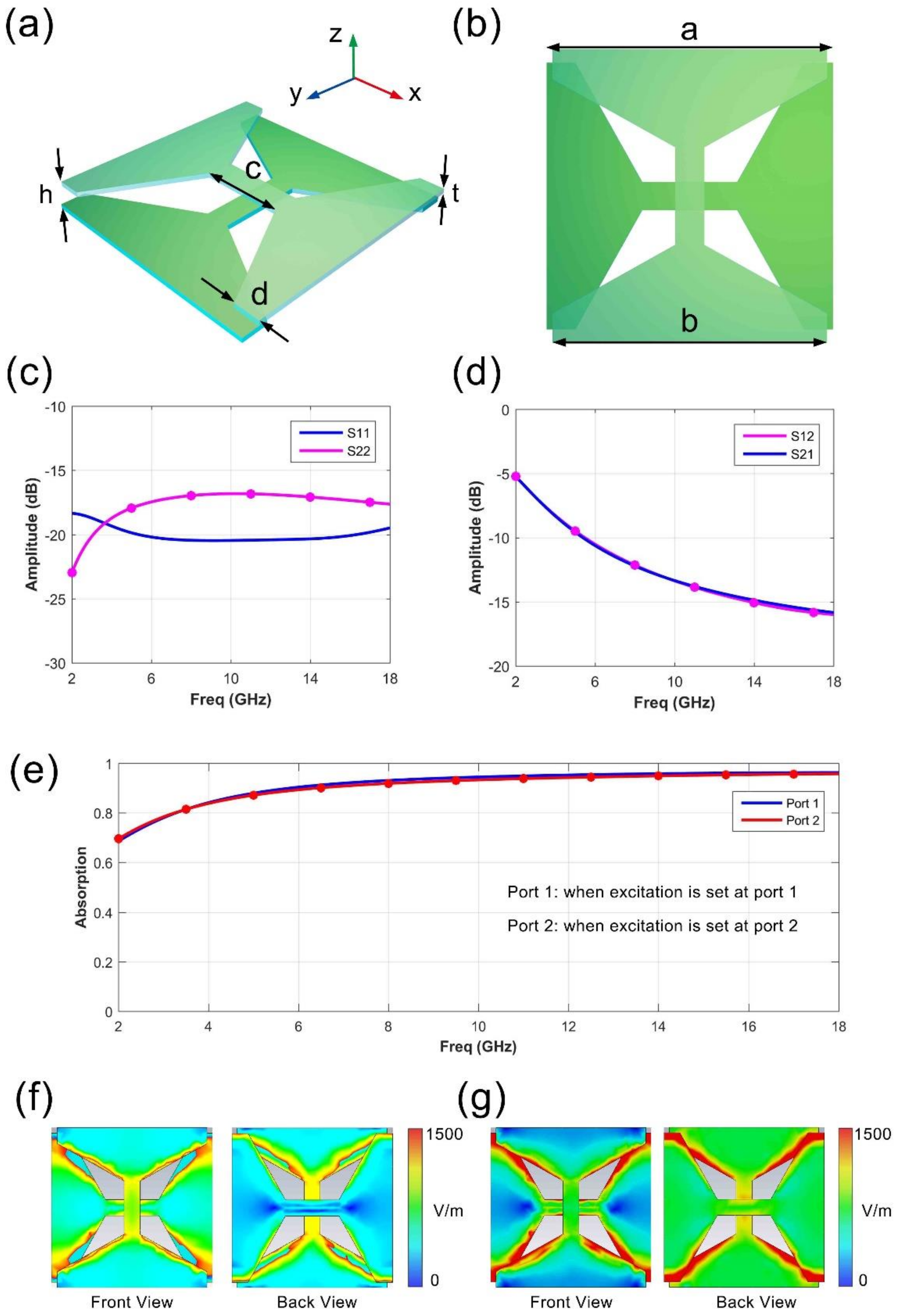
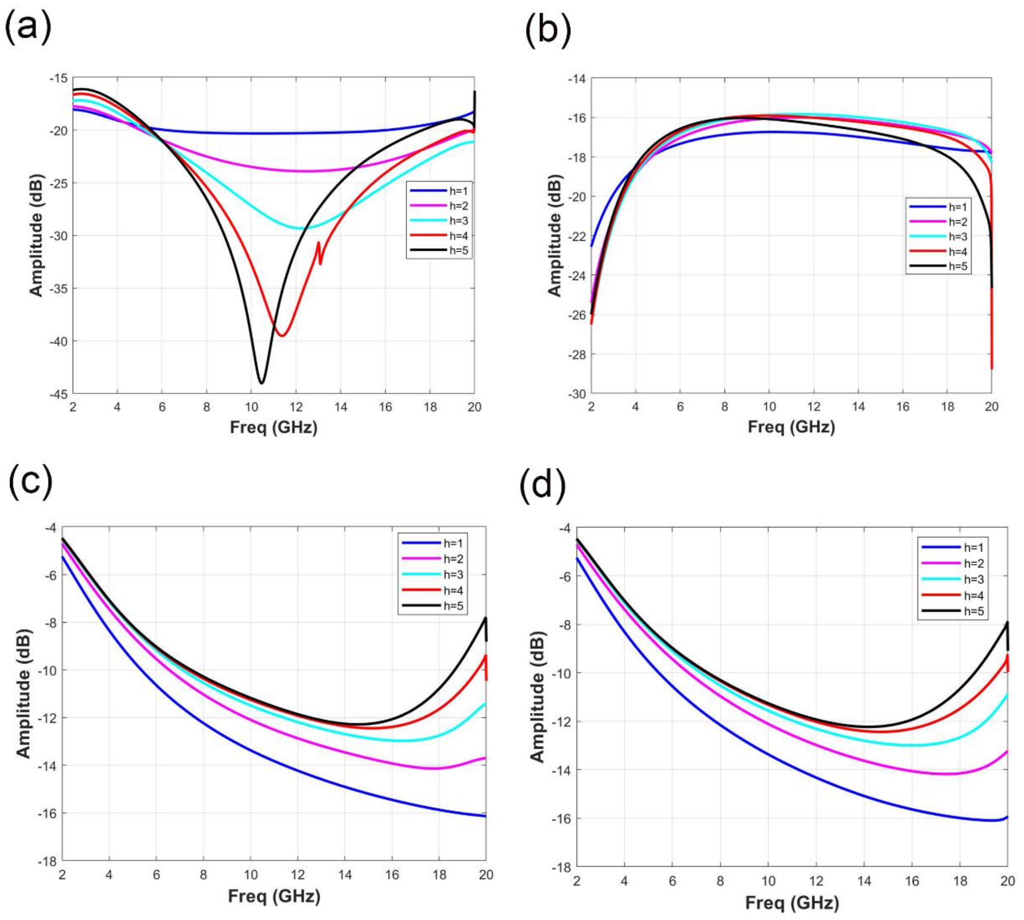
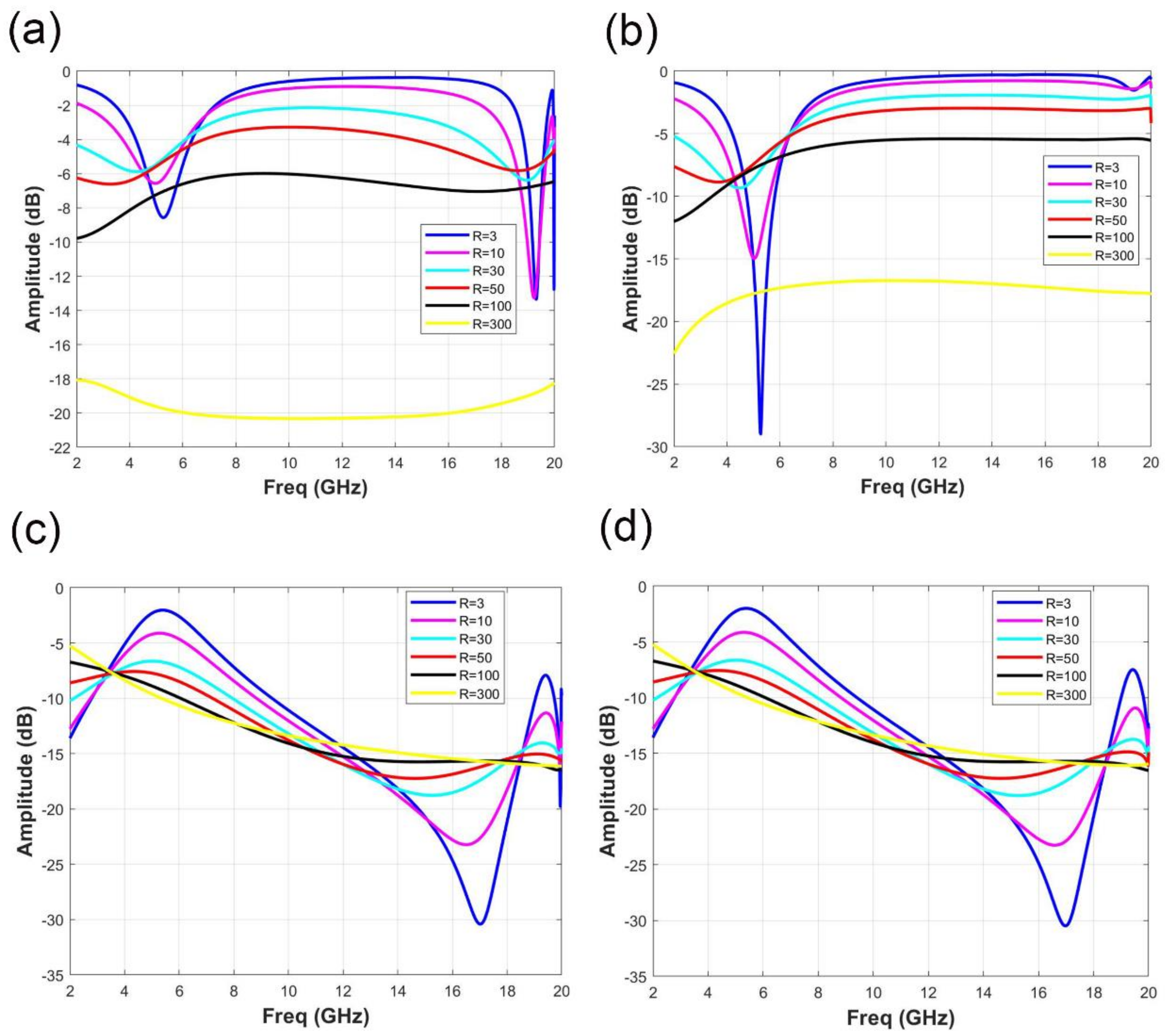
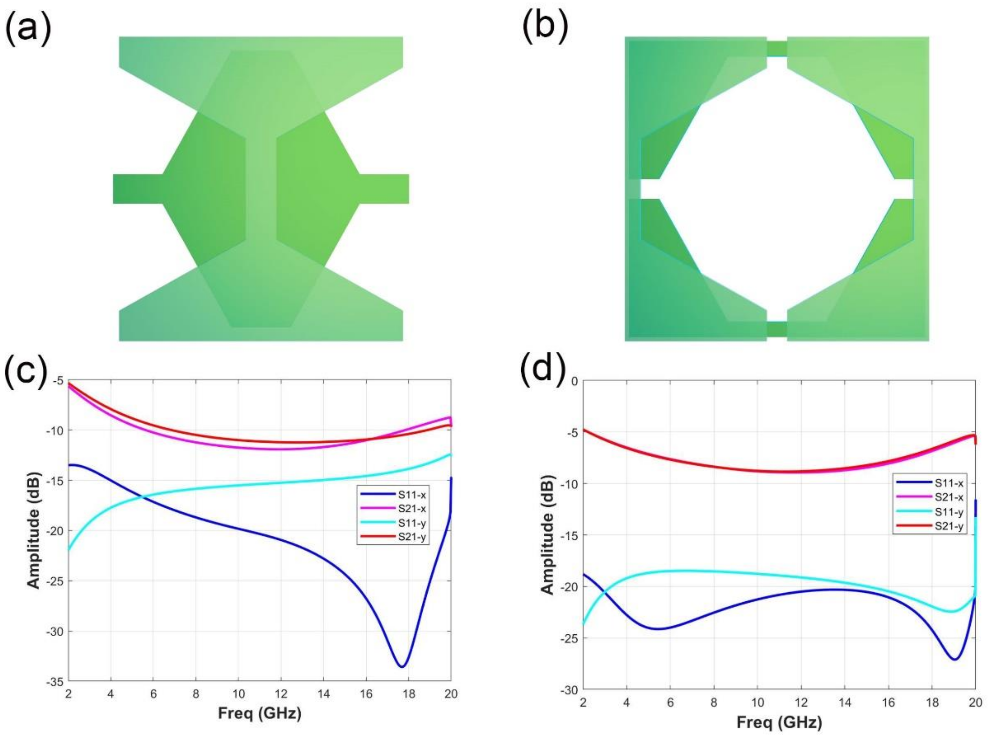
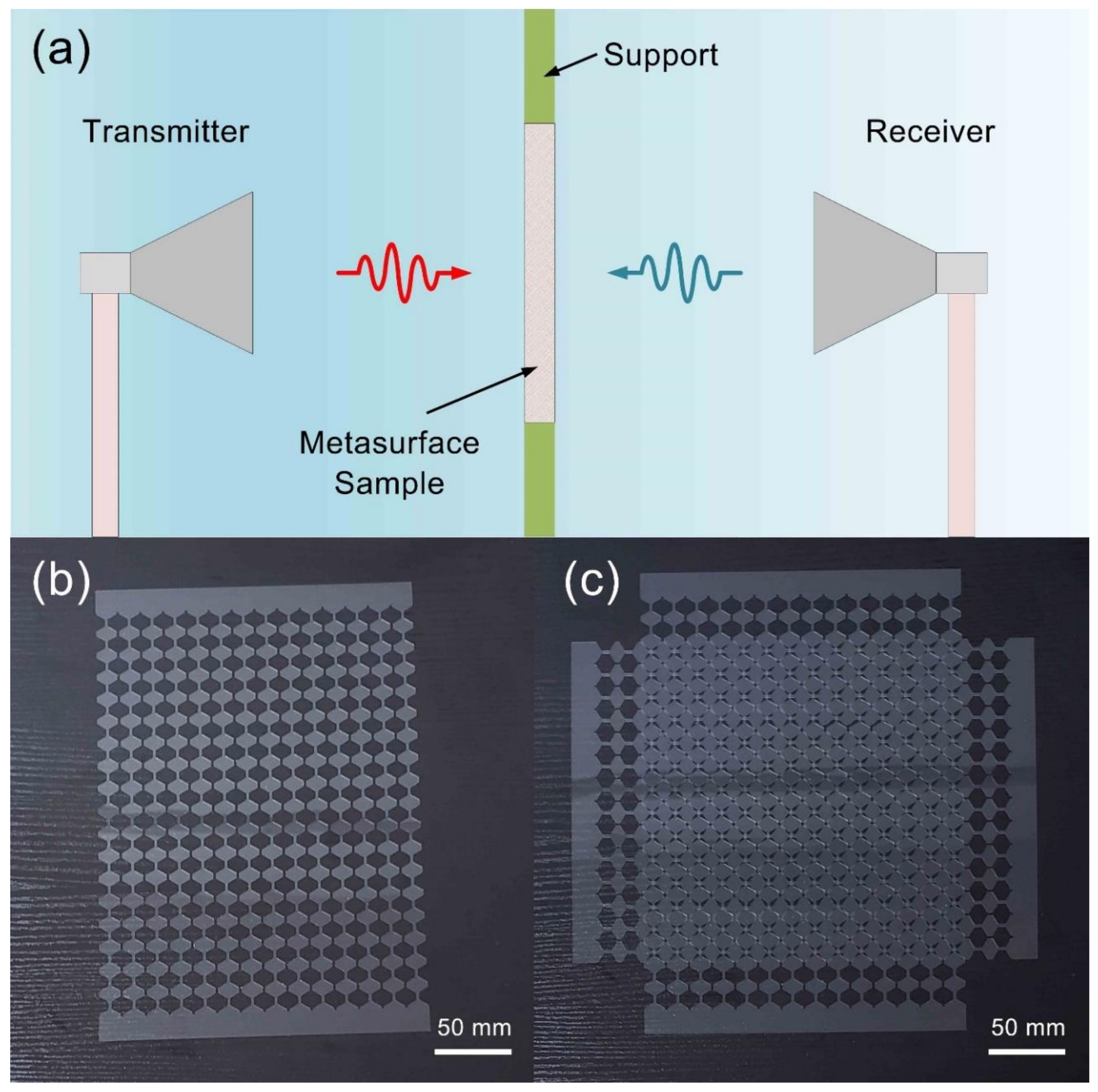
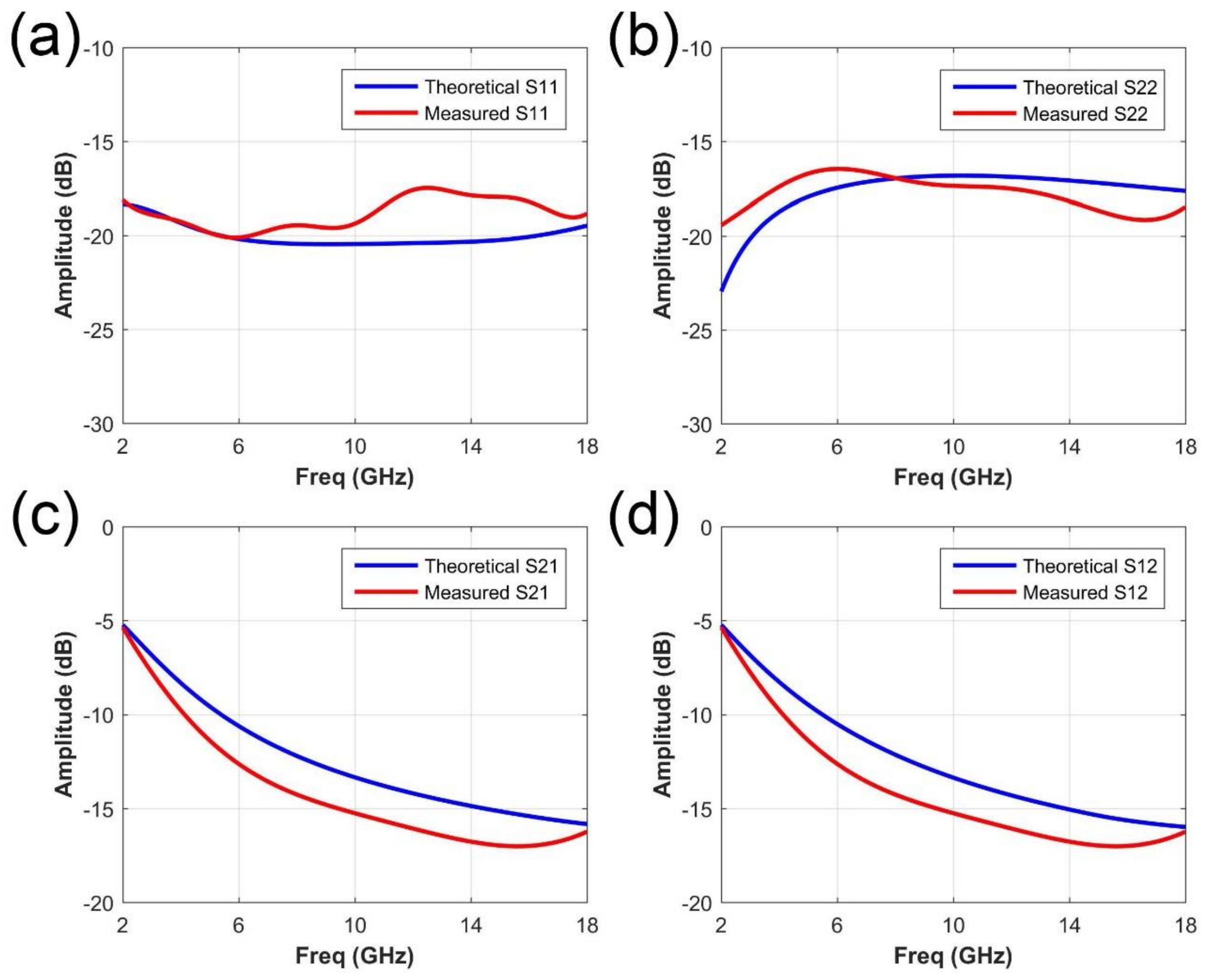
2. Design and Results
3. Discussion
Author Contributions
Funding
Conflicts of Interest
References
- Veselago, V.G. Electrodynamics of substances with simultaneously negative and μ. Sov. Phys. Uspekhi 1968, 10, 509–514. [Google Scholar] [CrossRef]
- Liberal, I.; Engheta, N. Near-zero refractive index photonics. Nat. Photonics 2017, 11, 149–158. [Google Scholar] [CrossRef]
- Hoffman, A.J.; Alekseyev, L.; Howard, S.S.; Franz, K.J.; Wasserman, D.; Podolskiy, V.A.; Narimanov, E.E.; Sivco, D.L.; Gmachl, C. Negative refraction in semiconductor metamaterials. Nat. Mater. 2007, 6, 946–950. [Google Scholar] [CrossRef]
- Pendry, J.B. Negative refraction makes a perfect lens. Phys. Rev. Lett. 2000, 85, 3966–3969. [Google Scholar] [CrossRef]
- Ma, Q.; Mei, Z.L.; Zhu, S.K.; Jin, T.Y.; Cui, T.J. Experiments on active cloaking and illusion for laplace equation. Phys. Rev. Lett. 2013, 111, 173901. [Google Scholar] [CrossRef]
- Ergin, T.; Stenger, N.; Brenner, P.; Pendry, J.B.; Wegener, M. Three-dimensional invisibility cloak at optical wavelengths. Science 2010, 328, 337–339. [Google Scholar] [CrossRef] [Green Version]
- Alù, A. Mantle cloak: Invisibility induced by a surface. Phys. Rev. B 2009, 80, 245115. [Google Scholar] [CrossRef]
- Ding, F.; Yang, Y.; Deshpande, R.A.; Bozhevolnyi, S.I. A review of gap-surface plasmon metasurfaces: Fundamentals and applications. Nanophotonics 2018, 7, 1129–1156. [Google Scholar] [CrossRef]
- Li, Z.; Rosenmann, D.; Czaplewski, D.A.; Yang, X.; Gao, J. Strong circular dichroism in chiral plasmonic metasurfaces optimized by micro-genetic algorithm. Opt. Express 2019, 27, 28313–28323. [Google Scholar] [CrossRef]
- Zhong, S.; Wu, L.; Liu, T.; Huang, J.; Jiang, W.; Ma, Y. Transparent transmission-selective radar-infrared bi-stealth structure. Opt. Express 2018, 26, 16466–16476. [Google Scholar] [CrossRef]
- Ma, Q.; Bai, G.D.; Jing, H.B.; Yang, C.; Li, L.; Cui, T.J. Smart metasurface with self-adaptively reprogrammable functions. Light Sci. Appl. 2019, 8, 1–12. [Google Scholar] [CrossRef] [Green Version]
- Ma, Q.; Hong, Q.R.; Gao, X.X.; Jing, H.B.; Liu, C.; Bai, G.D.; Cheng, Q.; Cui, T.J. Smart sensing metasurface with self-defined functions in dual polarizations. Nanophotonics 2020, 9, 20200052. [Google Scholar] [CrossRef]
- Chen, L.; Ruan, Y.; Cui, H.Y. Liquid metal metasurface for flexible beam-steering. Opt. Express 2019, 27, 23282–23292. [Google Scholar] [CrossRef]
- Chen, L.; Ma, Q.; Jing, H.B.; Cui, H.Y.; Liu, Y.; Cui, T.J. Space-energy digital-coding metasurface based on an active amplifier. Phys. Rev. Appl. 2019, 11, 054051. [Google Scholar] [CrossRef]
- Ma, Q.; Chen, L.; Jing, H.B.; Hong, Q.R.; Cui, H.Y.; Liu, Y.; Li, L.; Cui, T.J. Controllable and programmable nonreciprocity based on detachable digital coding metasurface. Adv. Opt. Mater. 2019, 7, 1901285. [Google Scholar] [CrossRef]
- Ma, Q.; Hong, Q.R.; Bai, G.D.; Jing, H.B.; Wu, R.Y.; Bao, L.; Cheng, Q.; Cui, T.J. Editing arbitrarily linear polarizations using programmable metasurface. Phys. Rev. Appl. 2020, 13, 021003. [Google Scholar] [CrossRef]
- Yu, N.F.; Genevet, P.; Kats, M.A.; Aieta, F.; Tetienne, J.P.; Capasso, F.; Gaburro, Z. Light propagation with phase discontinuities: Generalized laws of reflection and refraction. Science 2011, 334, 333–337. [Google Scholar] [CrossRef] [Green Version]
- Ma, Q.; Shi, C.B.; Bai, G.D.; Chen, T.Y.; Noor, A.; Cui, T.J. Beam-editing coding metasurfaces based on polarization bit and orbital-angular-momentum-mode bit. Adv. Opt. Mater. 2017, 5, 1700548. [Google Scholar] [CrossRef]
- Zhen, Q.; Zhen, Y.W.; Guo, Q.X.; Jian, W.; Lie, J.Q.; Dian, Y.F. Multi-vortex laser enabling spatial and temporal encoding. PhotoniX 2020, 1, 1–14. [Google Scholar]
- Li, L.; Cui, T.J.; Ji, W.; Liu, S.; Ding, J.; Wan, X.; Li, Y.B.; Jiang, M.H.; Qiu, C.W.; Zhang, S. Electromagnetic reprogrammable coding-metasurface holograms. Nat. Commun. 2017, 8, 197. [Google Scholar] [CrossRef] [Green Version]
- Wu, C.Y.; Lu, S.P.; Yang, Z.; Yashchyshyn, Y. A UWB absorber based on the TCA concept in the UHF band. IEEE Trans. Antenn. Propag. 2020, 68, 4132–4136. [Google Scholar] [CrossRef]
- Kaur, M.; Singh, H.S. Design and analysis of a compact ultrathin polarization- and incident angle-independent triple band metamaterial absorber. Microw. Opt. Techn. Let. 2020, 62, 1920–1929. [Google Scholar] [CrossRef]
- Barde, C.; Choubey, A.; Sinha, R. Wide band metamaterial absorber for Ku and K band applications. J. Appl. Phys. 2019, 126, 175104. [Google Scholar] [CrossRef]
- Yao, Z.X.; Xiao, S.Q.; Jiang, Z.G.; Yan, L.; Wang, B.Z. On the design of ultrawideband circuit analog absorber based on quasi-single-layer FSS. IEEE Antenn. Wirel. Propag. Lett. 2020, 19, 591–595. [Google Scholar] [CrossRef]
- Hannan, S.; Islam, M.T.; Hoque, A.; Singh, M.J.; Almutairi, A.F. Design of a novel double negative metamaterial absorber atom for Ku and K band applications. Electronics 2019, 8, 853. [Google Scholar] [CrossRef] [Green Version]
- Zhang, M.X.; Zhang, B.C.; Liu, X.C.; Sun, S.N.; Jin, C. Design of wideband absorber based on dual-resistor-loaded metallic strips. Int. J. Antenn. Propag. 2020, 2020. [Google Scholar] [CrossRef]
- Chen, M.; Chen, C.; Deng, S.J.; Wang, C.Y.; Liu, H.Q.; Teng, C.X.; Cheng, Y.; Yang, H.Y.; Xu, R.H.; Deng, H.C.; et al. Coherent perfect absorber based on antisymmetric metasurface with gain material. IEEE Photonics J. 2020, 12, 4500609. [Google Scholar] [CrossRef]
- Ren, Z.B.; Lin, Z.H.; Li, M.M.; Liu, R.Y.; Liu, T.X. Simple structured broadband metamaterial absorbers with the same topology and structural ratio for selected wavebands. Infrared Phys. Technol. 2020, 108, 103339. [Google Scholar] [CrossRef]
- Ding, F.; Dai, J.; Chen, Y.; Zhu, J.; Jin, Y.; Bozhevolnyi, S.I. Broadband near-infrared metamaterial absorbers utilizing highly lossy metals. Sci. Rep. 2016, 6, 39445. [Google Scholar] [CrossRef] [Green Version]
- Jain, P.; Bansal, S.; Prakash, K.; Sardana, N.; Gupta, N.; Kumar, S.; Singh, A.K. Graphene-based tunable multi-band metamaterial polarization-insensitive absorber for terahertz applications. J. Mater. Sci. Mater. Electron. 2020, 31, 11878–11886. [Google Scholar] [CrossRef]
- Jain, P.; Singh, A.K.; Pandey, J.K.; Garg, S.; Bansal, S.; Agarwal, M.; Kumar, S.; Sardana, N.; Gupta, N.; Singh, A.K. Ultra-thin metamaterial perfect absorbers for single-/dual-/multi-band microwave applications. IET Microw. Antenna. Propag. 2020, 14, 390–396. [Google Scholar] [CrossRef]
- Guo, W.; Liu, Y.; Han, T. Ultra-broadband infrared metasurface absorber. Opt. Express 2016, 24, 20586–20592. [Google Scholar] [CrossRef]
- Chen, F.; Cheng, Y.; Luo, H. A broadband tunable terahertz metamaterial absorber based on single-layer complementary gammadion-shaped graphene. Materials 2020, 13, 860. [Google Scholar] [CrossRef] [Green Version]
- Chen, L.; Ma, H.L.; Song, X.J.; Ruan, Y.; Cui, H.Y. Dual-functional tunable coding metasurface based on saline water substrate. Sci. Rep. 2018, 8, 2070. [Google Scholar] [CrossRef] [Green Version]
- Pang, Y.Q.; Wang, J.F.; Cheng, Q.; Xia, S.; Zhou, X.Y.; Xu, Z.; Cui, T.J.; Qu, S.B. Thermally tunable water-substrate broadband metamaterial absorbers. Appl. Phys. Lett. 2017, 110, 104103. [Google Scholar] [CrossRef]
- Wang, R.X.; Li, L.; Guo, T.; Wang, T.Z.; Liu, J.L.; Tian, H.; Tian, F.J.; Sun, W.M. Graphene/liquid crystal hybrid tuning terahertz perfect absorber. Appl. Opt. 2019, 58, 9406–9410. [Google Scholar] [CrossRef]
- Baier, M.; Grote, N.; Moehrle, M.; Sigmund, A.; Soares, F.M.; Theurer, M.; Troppenz, U. Integrated transmitter devices on InP exploiting electro-absorption modulation. PhotoniX 2020, 1, 4. [Google Scholar] [CrossRef]
- Cui, T.J.; Liu, S.; Bai, G.D.; Ma, Q. Direct transmission of digital message via programmable coding metasurface. Research 2019, 2019, 2584509. [Google Scholar] [CrossRef] [Green Version]
- Zou, X.J.; Wang, S.M.; Wang, Z.L.; Zhu, S.N. Imaging based on metalenses. PhotoniX 2020, 1, 2. [Google Scholar] [CrossRef] [Green Version]
- Araromi, A.; Graule, M.A.; Dorsey, K.L.; Castellanos, S.; Foster, J.R.; Hsu, W.H.; Passy, A.E.; Vlassak, J.J.; Weaver, J.C.; Walsh, C.J.; et al. Ultra-sensitive and resilient compliant strain gauges for soft machines. Nature 2020, 587, 219–224. [Google Scholar] [CrossRef]
- Gubbi, J.; Buyya, R.; Marusic, S.; Palaniswami, M. Internet of Things (IoT): A vision, architectural elements, and future directions. Future Gener. Comput. Syst. 2013, 29, 1645–1660. [Google Scholar] [CrossRef] [Green Version]


Publisher’s Note: MDPI stays neutral with regard to jurisdictional claims in published maps and institutional affiliations. |
© 2020 by the authors. Licensee MDPI, Basel, Switzerland. This article is an open access article distributed under the terms and conditions of the Creative Commons Attribution (CC BY) license (http://creativecommons.org/licenses/by/4.0/).
Share and Cite
Chen, L.; Ruan, Y.; Luo, S.S.; Ye, F.J.; Cui, H.Y. Optically Transparent Metasurface Absorber Based on Reconfigurable and Flexible Indium Tin Oxide Film. Micromachines 2020, 11, 1032. https://doi.org/10.3390/mi11121032
Chen L, Ruan Y, Luo SS, Ye FJ, Cui HY. Optically Transparent Metasurface Absorber Based on Reconfigurable and Flexible Indium Tin Oxide Film. Micromachines. 2020; 11(12):1032. https://doi.org/10.3390/mi11121032
Chicago/Turabian StyleChen, Lei, Ying Ruan, Si Si Luo, Fu Ju Ye, and Hao Yang Cui. 2020. "Optically Transparent Metasurface Absorber Based on Reconfigurable and Flexible Indium Tin Oxide Film" Micromachines 11, no. 12: 1032. https://doi.org/10.3390/mi11121032