Lift-Off Assisted Patterning of Few Layers Graphene

 , , , and
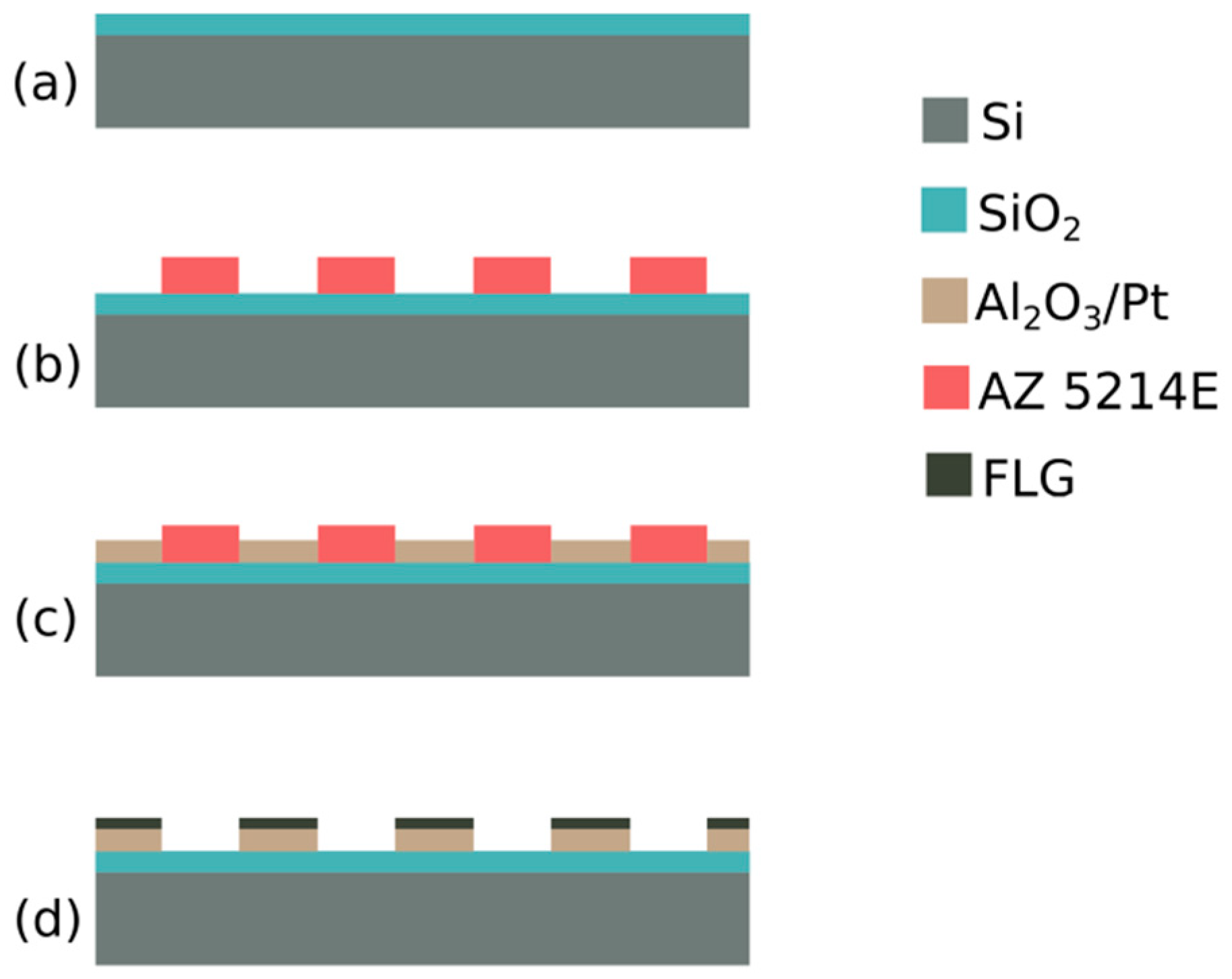
Abstract
:1. Introduction
2. Materials and Methods
2.1. Lift-Off Assisted Patterning
2.2. Graphene Deposition on Pt Film
2.3. Characterization
3. Results
3.1. Morphologica Characterization of De-Wetting Dynamic
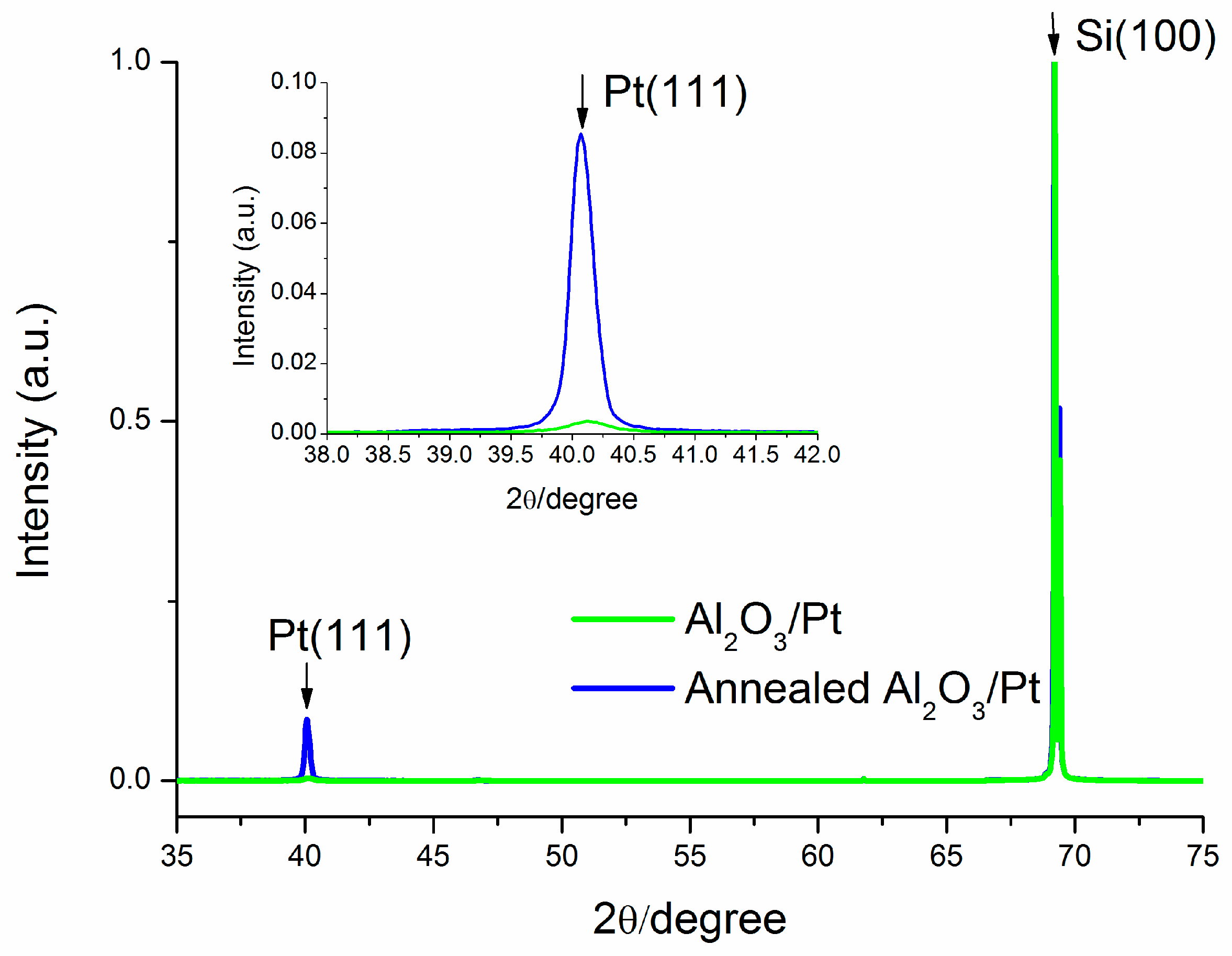
3.2. XRD Characterization
3.3. Raman Characterization of Patterned Pt
4. Discussion
5. Conclusions
Supplementary Materials
Author Contributions
Funding
Conflicts of Interest
References
- Dragoman, M.; Dragoman, D. Graphene-based quantum electronics. Prog. Quantum Electron. 2009, 33, 165–214. [Google Scholar] [CrossRef]
- Marasso, S.L.; Rivolo, P.; Giardi, R.; Mombello, D.; Gigot, A.; Serrapede, M.; Benetto, S.; Enrico, A.; Cocuzza, M.; Tresso, E.; et al. A novel graphene based nanocomposite for application in 3D flexible micro-supercapacitors. Mater. Res. Express 2016, 3, 065001. [Google Scholar] [CrossRef]
- Hill, E.W.; Vijayaragahvan, A.; Novoselov, K. Graphene sensors. IEEE Sens. J. 2011, 11, 3161–3170. [Google Scholar] [CrossRef]
- Podila, R.; Moore, T.; Alexis, F.; Rao, A. Graphene Coatings for Biomedical Implants. J. Vis. Exp. 2013, 73, 1–9. [Google Scholar] [CrossRef] [PubMed]
- Zhang, Y.I.; Zhang, L.; Zhou, C. Review of Chemical Vapor Deposition of Graphene and Related Applications. Acc. Chem. Res. 2013, 46, 2329–2339. [Google Scholar] [CrossRef] [PubMed]
- Ghorban Shiravizadeh, A.; Elahi, S.M.; Sebt, S.A.; Yousefi, R. High performance of visible-NIR broad spectral photocurrent application of monodisperse PbSe nanocubes decorated on rGO sheets. J. Appl. Phys. 2018, 123, 083102. [Google Scholar] [CrossRef]
- Barin, G.B.; Song, Y.; Gimenez, I.D.F.; Filho, A.G.S.; Barreto, L.S.; Kong, J. Optimized graphene transfer: Influence of polymethylmethacrylate (PMMA) layer concentration and baking time on grapheme final performance. Carbon 2015, 84, 82–90. [Google Scholar] [CrossRef]
- Song, J.; Kam, F.; Png, R.; Seah, W.; Zhuo, J.; Lim, G.; Ho, P.K.H.; Chua, L. A general method for transferring graphene onto soft surfaces. Nat. Nanotechnol. 2013, 8, 356–362. [Google Scholar] [CrossRef]
- Lee, Y.; Bae, S.; Jang, H.; Jang, S.; Zhu, S.-E.; Sim, S.H.; Song, Y.I.; Hong, B.H.; Ahn, J.-H. Wafer-Scale Synthesis and Transfer of graphene films. Nano Lett. 2010, 10, 490–493. [Google Scholar] [CrossRef]
- Gao, L.; Ren, W.; Xu, H.; Jin, L.; Wang, Z.; Ma, T.; Ma, L.; Zhang, Z.; Fu, Q.; Peng, L.; et al. Repeated growth and bubbling transfer of graphene with millimetre-size single-crystal grains using platinum. Nat. Commun. 2012, 3, 699. [Google Scholar] [CrossRef]
- Gao, L.; Ni, G.-X.; Liu, Y.; Liu, B.; Castro Neto, A.H.; Loh, K.P. Face-to-face transfer of wafer-scale graphene films. Nature 2013, 505, 190–194. [Google Scholar] [CrossRef] [PubMed]
- Kim, H.; Song, I.; Park, C.; Son, M.; Hong, M.; Kim, Z.; Kim, J.S.; Shin, H.; Baik, J.; Choi, C. Copper-Vapor-Assisted Chemical Vapor Deposition for High-Quality and Metal-Free Single-Layer Graphene on Amorphous SiO2 Substrate. ACS Nano 2013, 7, 6575–6582. [Google Scholar] [CrossRef] [PubMed]
- Ismach, A.; Druzgalski, C.; Penwell, S.; Schwartzberg, A.; Zheng, M.; Javey, A.; Bokor, J.; Zhang, Y. Direct chemical vapor deposition of graphene on dielectric surfaces. Nano Lett. 2010, 10, 1542–1548. [Google Scholar] [CrossRef] [PubMed]
- Kaplas, T.; Sharma, D.; Svirko, Y. Few-layer graphene synthesis on a dielectric substrate. Carbon 2012, 50, 1503–1509. [Google Scholar] [CrossRef]
- Marchena, M.; Janner, D.; Chen, T.L.; Finazzi, V.; Pruneri, V. Low temperature direct growth of graphene patterns on flexible glass substrates catalysed by a sacrificial ultrathin Ni film. Opt. Mat. Express 2016, 6, 2487–2507. [Google Scholar] [CrossRef] [Green Version]
- Alexeev, A.M.; Barnes, M.D.; Nagareddy, V.K.; Craciun, M.F.; Wright, C.D. A simple process for the fabrication of large-area CVD graphene based devices via selective in situ functionalization and patterning. 2D Mater. 2016, 4, 011010. [Google Scholar] [CrossRef]
- Lanza, M.; Bayerl, A.; Gao, T.; Porti, M.; Nafria, M.; Jing, G.Y.; Zhang, Y.F.; Liu, Z.F.; Duan, H.L. Graphene-coated atomic force microscope tips for reliable nanoscale electrical characterization. Adv. Mater. 2013, 25, 1440–1444. [Google Scholar] [CrossRef]
- Klemenz, A.; Pastewka, L.; Balakrishna, S.G.; Caron, A.; Bennewitz, R.; Moseler, M. Atomic scale mechanisms of friction reduction and wear protection by graphene. Nano Lett. 2014, 14, 7145–7152. [Google Scholar] [CrossRef]
- Cheng, C.E.; Lin, C.Y.; Shan, C.H.; Tsai, S.Y.; Lin, K.W.; Chang, C.S.; Shih-Sen Chien, F. Platinum-graphene counter electrodes for dye-sensitized solar cells. J. Appl. Phys. 2013, 114, 014503. [Google Scholar] [CrossRef] [Green Version]
- Park, H.; Zhang, S.; Steinman, A.; Chen, Z.; Lee, H. Graphene prevents neurostimulation-induced platinum dissolution in fractal microelectrodes. 2D Mater. 2019, 6, 035037. [Google Scholar] [CrossRef] [Green Version]
- Lucca, B.G.; de Lima, F.; Coltro, W.K.T.; Ferreira, V.S. Electrodeposition of reduced graphene oxide on a Pt electrode and its use as amperometric sensor in microchip electrophoresis. Electrophoresis 2015, 36, 1886–1893. [Google Scholar] [CrossRef] [PubMed]
- Molina, J.; Fernández, J.; García, C.; Del Río, A.I.; Bonastre, J.; Cases, F. Electrochemical characterization of electrochemically reduced graphene coatings on platinum. Electrochemical study of dye adsorption. Electrochim. Acta 2015, 166, 54–63. [Google Scholar] [CrossRef]
- Gutés, A.; Hsia, B.; Sussman, A.; Mickelson, W.; Zettl, A.; Carraroa, C.; Maboudian, R. Graphene decoration with metal nanoparticles: Towards easy integration for sensing applications. Nanoscale 2012, 4, 438–440. [Google Scholar] [CrossRef] [PubMed]
- Huang, J.; Tian, J.; Zhao, Y.; Zhao, S. Ag/Au nanoparticles coated graphene electrochemical sensor for ultrasensitive analysis of carcinoembryonic antigen in clinical immunoassay. Sens. Actuators B Chem. 2015, 206, 570–576. [Google Scholar] [CrossRef]
- Shao, Y.; Wang, J.; Wu, H.; Liu, J.; Aksay, I.A.; Lin, Y. Graphene Based Electrochemical Sensors and Biosensors: A Review. Electroanalysis 2010, 22, 1027–1036. [Google Scholar] [CrossRef]
- Yuan, W.; Shi, G. Graphene-based gas sensors. J. Mater. Chem. A 2013, 1, 10078–10091. [Google Scholar] [CrossRef]
- Pérez-Mas, A.M.; Álvarez, P.; Campos, N.; Gómez, D.; Menéndez, R. Graphene patterning by nanosecond laser ablation: The effect of the substrate interaction with graphene. J. Phys. D. Appl. Phys. 2016, 49, 305301. [Google Scholar] [CrossRef]
- Feng, J.; Li, W.; Qian, X.; Qi, J.; Qi, L.; Li, J. Patterning of graphene. Nanoscale 2012, 4, 4883–4899. [Google Scholar] [CrossRef] [PubMed]
- Sutter, P.; Sadowski, J.T.; Sutter, E. Graphene on Pt(111): Growth and substrate interaction. Phys. Rev. B 2009, 80, 1–10. [Google Scholar] [CrossRef]
- Kang, B.J.; Mun, J.H.; Hwang, C.Y.; Cho, B.J. Monolayer graphene growth on sputtered thin film platinum. J. Appl. Phys. 2009, 106, 104309. [Google Scholar] [CrossRef] [Green Version]
- Nam, J.; Kim, D.C.; Yun, H.; Shin, D.H.; Nam, S.; Lee, W.K.; Hwang, J.Y.; Lee, S.W.; Weman, H.; Kim, K.S. Chemical vapor deposition of graphene on platinum: Growth and substrate interaction. Carbon 2017, 111, 733–740. [Google Scholar] [CrossRef] [Green Version]
- Firebaugh, S.L.; Jensen, K.F.; Schmidt, M.A. Investigation of high-temperature degradation of platinum thin films with an in situ resistance measurement apparatus. J. Microelectromech. Syst. 1998, 7, 128–135. [Google Scholar] [CrossRef]
- Guarnieri, V.; Biazi, L.; Marchiori, R.; Lago, A. Platinum metallization for MEMS application: Focus on coating adhesion for biomedical applications. Biomatter 2014, 4, 2–8. [Google Scholar] [CrossRef] [PubMed]
- Madaan, N.; Kanyal, S.S.; Jensen, D.S.; Vail, M.A.; Dadson, A.E.; Engelhard, M.H.; Samha, H.; Linford, M.R. Al2O3 e-Beam Evaporated onto Silicon (100)/SiO2, by XPS. Surf. Sci. Spectra 2013, 20, 43–48. [Google Scholar] [CrossRef]
- Tarabella, G.; Balducci, A.G.; Coppedè, N.; Marasso, S.; D’Angelo, P.; Barbieri, S.; Cocuzza, M.; Colombo, P.; Sonvico, F.; Mosca, R.; et al. Liposome sensing and monitoring by organic electrochemical transistors integrated in microfluidics. Biochim. Biophys. Acta, Gen. Subj. 2013, 1830, 4374–4380. [Google Scholar] [CrossRef] [PubMed]
- Marasso, S.L.; Tommasi, A.; Perrone, D.; Cocuzza, M.; Mosca, R.; Villani, M.; Zappettini, A.; Calestani, D. A new method to integrate ZnO nano- tetrapods on MEMS micro-hotplates for large scale gas sensor production. Nanotechnology 2016, 27, 1–7. [Google Scholar] [CrossRef] [PubMed]
- Tommasi, A.; Cocuzza, M.; Perrone, D.; Pirri, C.; Mosca, R.; Villani, M.; Delmonte, N.; Zappettini, A.; Calestani, D.; Marasso, S. Modeling, Fabrication and Testing of a Customizable Micromachined Hotplate for Sensor Applications. Sensors 2016, 17, 62. [Google Scholar] [CrossRef] [PubMed]
- Wang, Y.; Ni, Z.; Yu, T.; Shen, Z.X.; Wang, H.; Wu, Y.; Chen, W.; Thye, A.; Wee, S. Raman Studies of Monolayer Graphene: The Substrate Effect. J. Phys. Chem. C 2008, 112, 10637–10640. [Google Scholar] [CrossRef]
- Hawaldar, R.; Merino, P.; Correia, M.R.; Bdikin, I.; Grácio, J.; Méndez, J.; Martín-Gago, J.A.; Singh, M.K. Large-area high-throughput synthesis of monolayer graphene sheet by Hot filament thermal chemical vapor deposition. Sci. Rep. 2012, 2, 2–10. [Google Scholar] [CrossRef]
- Ferrari, A.C.; Basko, D.M. Raman spectroscopy as a versatile tool for studying the properties of graphene. Nat. Nanotechnol. 2013, 8, 235–246. [Google Scholar] [CrossRef] [Green Version]
- Park, H.J.; Meyer, J.; Roth, S.; Skákalová, V. Growth and properties of few-layer graphene prepared by chemical vapor deposition. Carbon 2010, 48, 1088–1094. [Google Scholar] [CrossRef] [Green Version]
- Jerng, S.-K.; Seong Yu, D.; Hong Lee, J.; Kim, C.; Yoon, S.; Chun, S.-H. Graphitic carbon growth on crystalline and amorphous oxide substrates using molecular beam epitaxy. Nanoscale Res. Lett. 2011, 6, 565. [Google Scholar] [CrossRef] [PubMed]


© 2019 by the authors. Licensee MDPI, Basel, Switzerland. This article is an open access article distributed under the terms and conditions of the Creative Commons Attribution (CC BY) license (http://creativecommons.org/licenses/by/4.0/).
Share and Cite
Verna, A.; Marasso, S.L.; Rivolo, P.; Parmeggiani, M.; Laurenti, M.; Cocuzza, M. Lift-Off Assisted Patterning of Few Layers Graphene. Micromachines 2019, 10, 426. https://doi.org/10.3390/mi10060426
Verna A, Marasso SL, Rivolo P, Parmeggiani M, Laurenti M, Cocuzza M. Lift-Off Assisted Patterning of Few Layers Graphene. Micromachines. 2019; 10(6):426. https://doi.org/10.3390/mi10060426
Chicago/Turabian StyleVerna, Alessio, Simone Luigi Marasso, Paola Rivolo, Matteo Parmeggiani, Marco Laurenti, and Matteo Cocuzza. 2019. "Lift-Off Assisted Patterning of Few Layers Graphene" Micromachines 10, no. 6: 426. https://doi.org/10.3390/mi10060426