Fabrications of L-Band LiNbO3-Based SAW Resonators for Aerospace Applications

 ,
,
Abstract
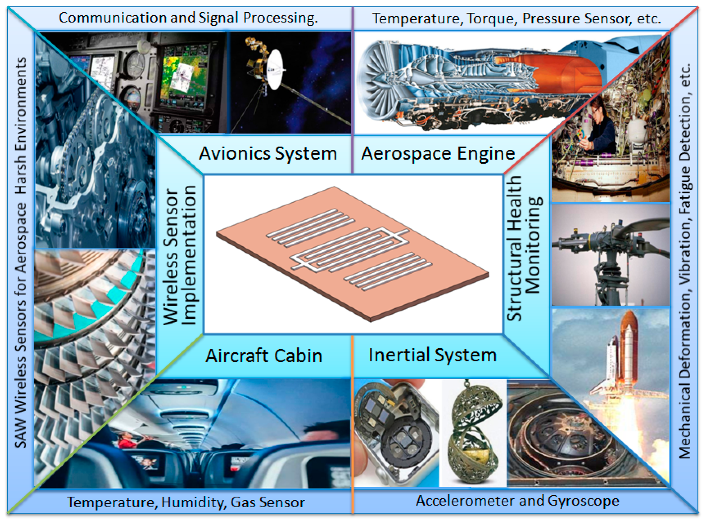
:1. Introduction
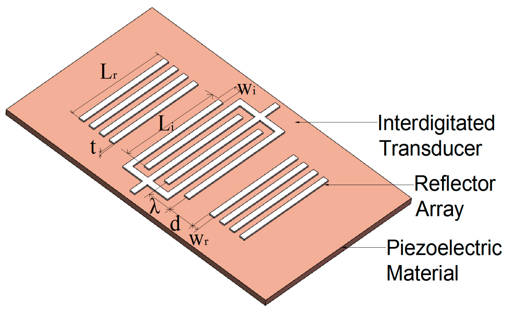
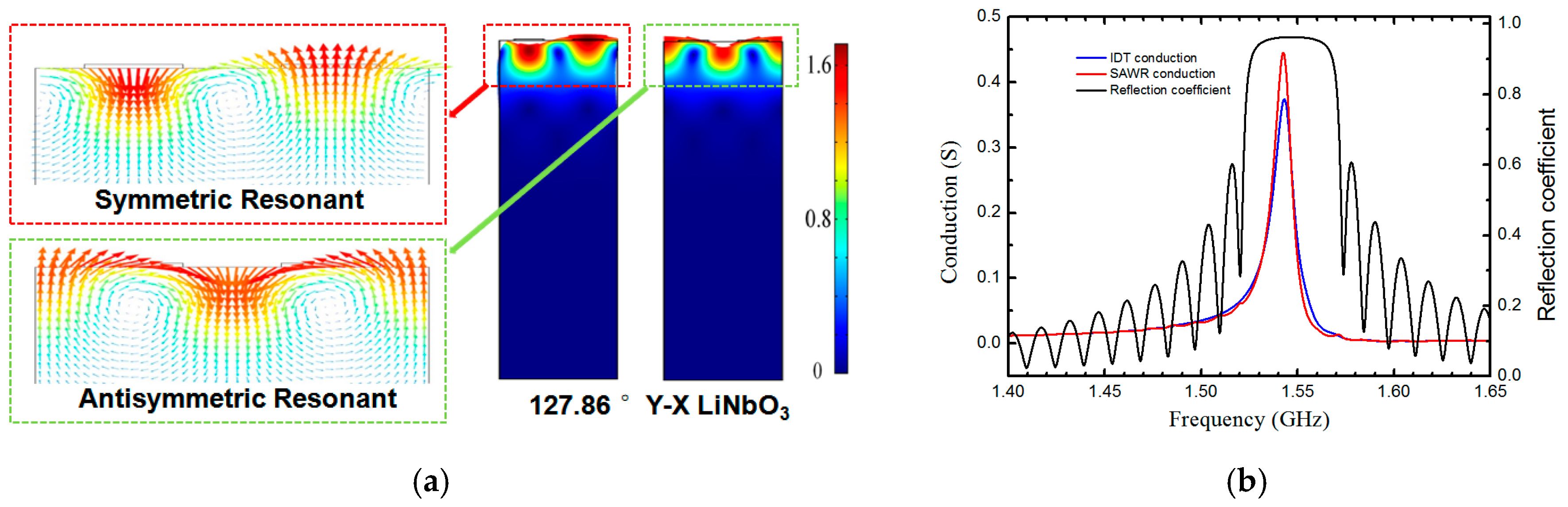
2. Design and Simulation Single-Port SAW Resonator
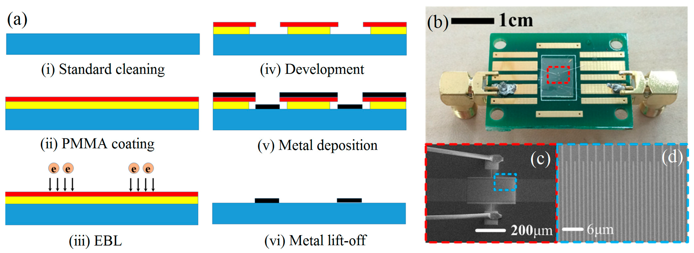
3. Fabrication and Testing of SAW Resonator
4. Results and Discussion
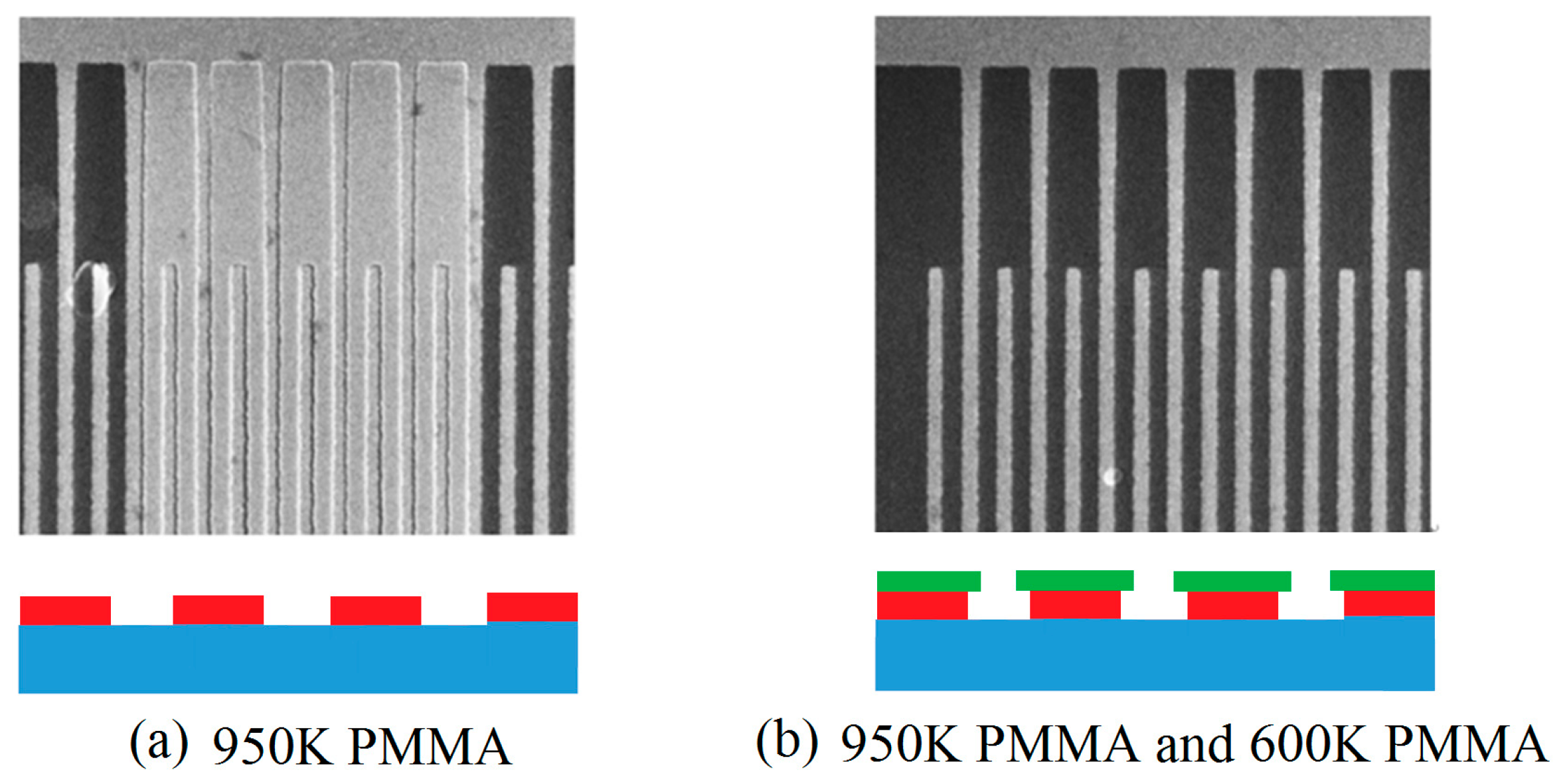
4.1. Effect of Electron Beam Resist on Fabrication Quality
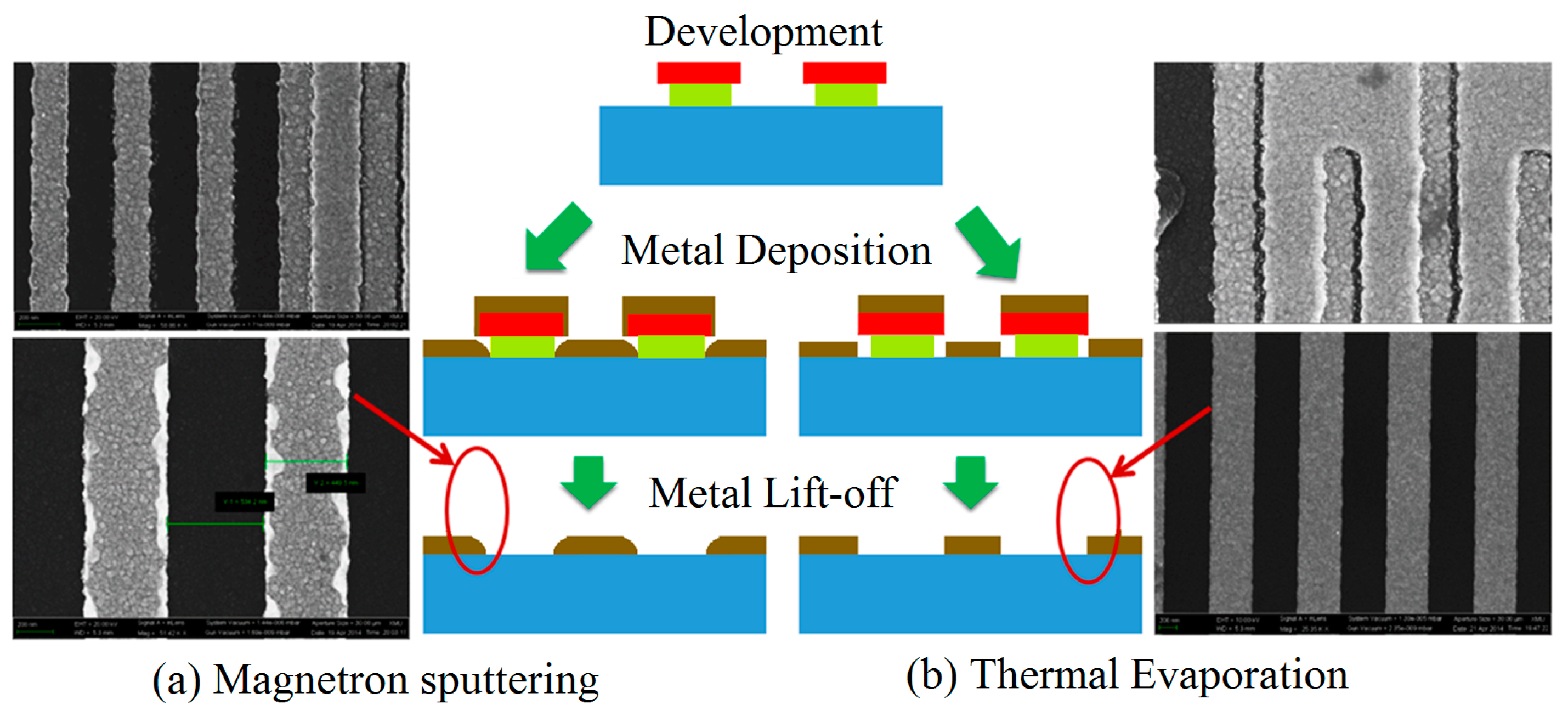
4.2. Effect of Metal Film Deposition Processes on Metal Lift-Off
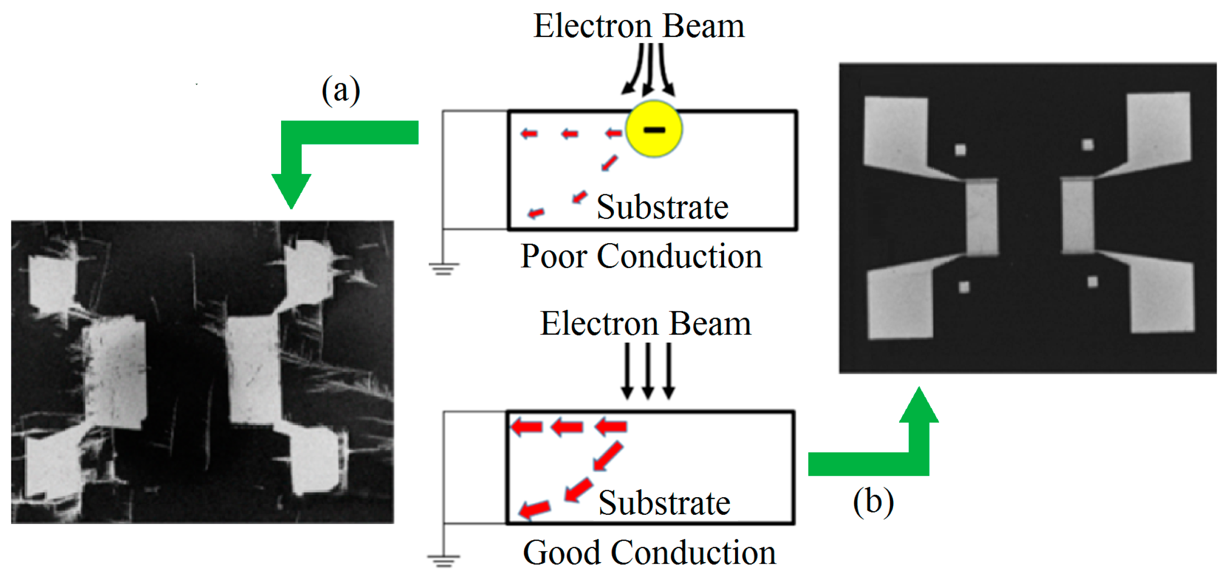
4.3. Effect of Charge Accumulation on Exposure Precision
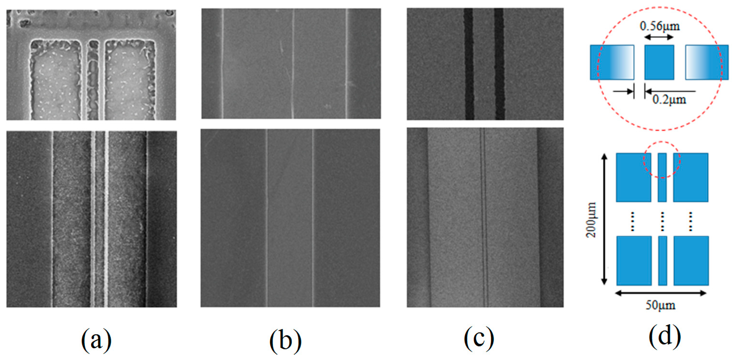
4.4. Correction of Proximity Effect
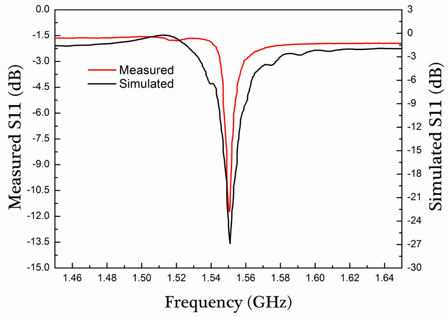
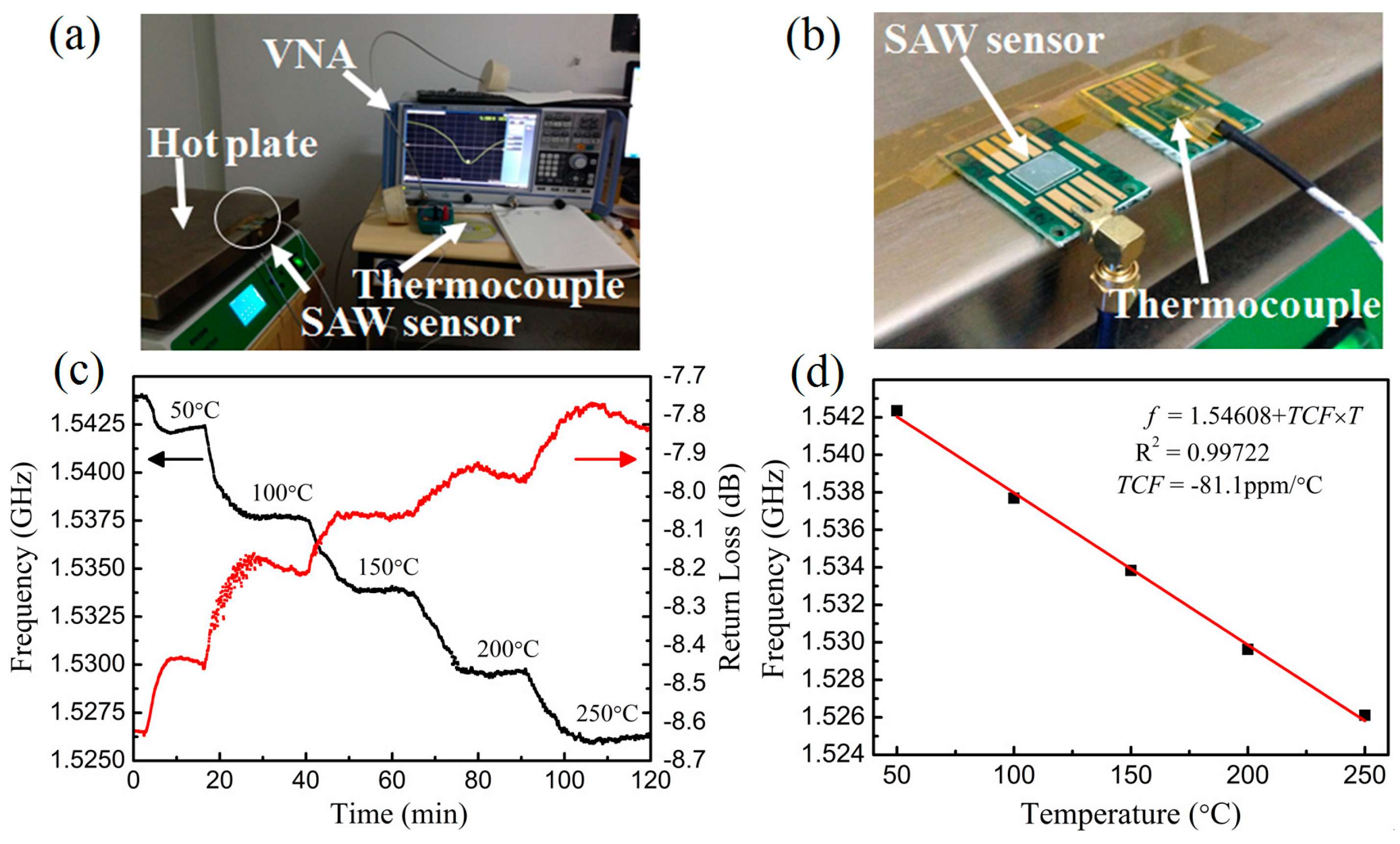
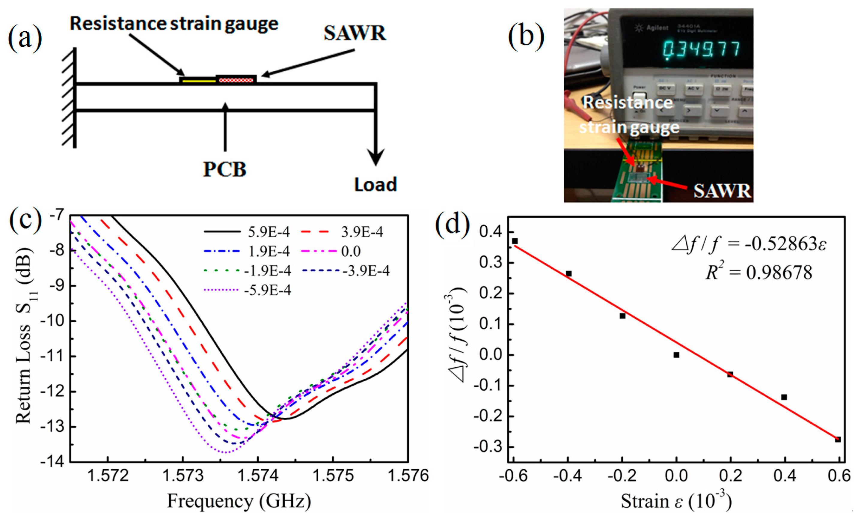
4.5. Characterization and Sensing Properties of SAW Devices
5. Conclusions
Author Contributions
Funding
Conflicts of Interest
References
- Rayleigh, L. On waves propagated along the plane surface of an elastic solid. Proc. Lond. Math. Soc. 1885, 17, 4–11. [Google Scholar] [CrossRef]
- Müller, A.; Konstantinidis, G.; Buiculescu, V.; Dinescu, A.; Stavrinidis, A.; Stefanescu, A. GaN/Si based single SAW resonator temperature sensoroperating in the GHz frequency range. Sens. Actuators A 2014, 209, 115–123. [Google Scholar] [CrossRef]
- Binder, A.; Bruckner, G.; Schobernig, N.; Schmitt, D. Wireless surface acousticwave pressure and temperature sensor with unique identification based on LiNbO3. IEEE Sens. J. 2013, 13, 1801–1805. [Google Scholar] [CrossRef]
- Xuan, W.; He, M.; Meng, N.; He, X.; Wang, W.; Chen, J.; Shi, T.; Hasan, T.; Xu, H.; Xu, Y.X.; et al. Fast response and high sensitivity ZnO/glass surface acoustic wave humidity sensors using graphene oxide sensing layer. Sci. Rep. 2014, 4, 7206. [Google Scholar] [CrossRef] [PubMed]
- Stoney, R.; Geraghty, D.; O’Donnell, G.E. Characterization of differentially measured strain using passive wireless surface acoustic wave (SAW) strain sensors. IEEE Sens. J. 2014, 14, 722–728. [Google Scholar] [CrossRef]
- Wang, Y.; Chyu, M.K.; Wang, Q.M. Passive wireless surface acoustic wave CO2 sensor with carbon nanotube nanocomposite as an interface layer. Sens. Actuators A 2014, 220, 34–44. [Google Scholar] [CrossRef]
- Kuo, F.Y.; Lin, Y.C.; Ke, L.Y.; Tsai, C.J.; Yao, D.J. Detection of Particulate Matter of Size 2.5 μm with a Surface-Acoustic-Wave Sensor Combined with a Cyclone Separator. Micromachines 2018, 9, 398. [Google Scholar] [CrossRef]
- Wilson, W.C.; Malocha, D.C.; Kozlovski, N.; Gallagher, D.R.; Fisher, B.; Pavlina, J.; Saldanha, N.; Puccio, D.; Atkinson, G.M. Orthogonal Frequency Coded SAW Sensors for Aerospace SHM Applications. IEEE Sens. J. 2009, 9, 1546–1556. [Google Scholar] [CrossRef]
- Greve, D.; Chin, T.L.; Zheng, P.; Ohodnicki, P.; Baltrus, J.; Oppenheim, I.J. Surface acoustic wave devices for harsh environment wireless sensing. Sensors 2013, 13, 6910–6935. [Google Scholar] [CrossRef]
- Adnan, M.; Franz, D. Surface Acoustic Wave (SAW) for Chemical Sensing Applications of Recognition Layers. Sensors 2017, 17, 2716. [Google Scholar]
- Ruppel, C.C.W. Acoustic Wave Filter Technology–A Review. IEEE Trans. Ultrason. Ferroelectr. Freq. Control 2017, 64, 1390–1400. [Google Scholar] [CrossRef] [PubMed]
- Pasternak, M. Overtone oscillator for SAW gas detectors. IEEE Sens. J. 2006, 6, 1497–1501. [Google Scholar]
- Rodríguez-Madrid, J.G.; Iriarte, G.F.; Pedrós, J.; Williams, O.A.; Brink, D.; Calle, F. Super-High-Frequency SAW Resonators on AlN/Diamond. IEEE Electr. Device Lett. 2012, 33, 495–497. [Google Scholar] [CrossRef]
- Hatakeyama, H.; Omori, T.; Hashimoto, K.Y.; Yamayuchi, M. Fabrication of SAW Devices Using SEM-Based Electron Beam Lithography and Lift-off Technique for Lab Use. Proc. IEEE Ultrason. Symp. 2004, 3, 1896–1900. [Google Scholar]
- Rodríguez-Madrid, J.G.; Iriarte, G.F.; Araujo, D.; Villar, M.P.; Williams, O.A.; Müller-Sebert, W.; Calle, F. Optimization of AlN thin layers on diamond substrates for high frequency SAW resonators. Mater. Lett. 2012, 66, 339–342. [Google Scholar] [CrossRef] [Green Version]
- Aubert, T.; Elmazria, O.; Assouar, B.; Blampain, E.; Hamdan, A.; Genève, D.; Weber, S. Investigations on AlN/Sapphire Piezoelectric Bilayer Structure for High-Temperature SAW Applications. IEEE Trans. Ultrason. Ferroelectr. Freq. Control 2012, 59, 999–1005. [Google Scholar] [CrossRef]
- Lloret, F.; Araújo, D.; Villar, M.P.; Rodríguez-Madrid, J.G.; Iriarte, G.F.; Williams, O.A.; Calle, F. Diamond underlayer microstructure effect on the orientation of AlN piezoelectric layers for high frequency SAW resonators by TEM. Microelectron. Eng. 2013, 112, 193–197. [Google Scholar] [CrossRef]
- Tseng, A.A.; Chen, K.; Chen, C.D.; Ma, K.J. Electron Beam Lithography in Nanoscale Fabrication: Recent Development. IEEE Trans. Electron. Packag. Manuf. 2003, 26, 141–149. [Google Scholar] [CrossRef]
- Groves, T.R.; Pickard, D.; Rafferty, B.; Crosland, N.; Adam, D.; Schubert, G. Maskless electron beam lithography: Prospects, progress, and challenges. Microelectron. Eng. 2002, 61, 285–293. [Google Scholar] [CrossRef]
- Tırpancı, Ş.; Bürgler, D.E.; Schneider, C.M.; Rameev, B.; Aktaş, B. Charging effect reduction in electron beam lithography and observation of single nanopillars on highly insulating substrates. Microelectron. Eng. 2015, 140, 33–37. [Google Scholar] [CrossRef]
- Chen, Y. Nanofabrication by electron beam lithography and its applications: A review. Microelectron. Eng. 2015, 135, 57–72. [Google Scholar] [CrossRef]
- Madou, M.J. Fundamentals of Microfabrication: The Science of Miniaturization, 2nd ed.; CRC Press: Boca Raton, FL, USA, 2002. [Google Scholar]
- Auld, B.A. Acoustic Fields and Waves in Solids; Krieger Publishing Company: Malabar, FL, USA, 1990. [Google Scholar]
- Bell, D.T.; Li, R.C. IEEE 1976 Surface-Acoustic-Wave Resonators. Proc. IEEE 1976, 64, 711–721. [Google Scholar] [CrossRef]
- Hofer, M.; Finger, N.; Kovacs, G.; Schoeberl, J.; Langer, U.; Lervh, R. Finite Element Simulation of Bulk and Surface Acoustic Wave (SAW) Interaction in SAW Devices. In Proceedings of the IEEE Ultrasonics Symposium, Munich, Germany, 8–11 October 2002. [Google Scholar]
- Plessky, V. Coupling-Of-Modes Analysis of SAW Devices. Int. J. High Speed Electron. Syst. 2000, 10, 869–947. [Google Scholar] [CrossRef]
- Hashimoto, K.Y. Surface Acoustic Wave Devices in Telecommunications: Modelling and Simulation; Springer: New York, NY, USA, 2000. [Google Scholar]
- Li, P. Research on Passive Wireless Surface Acoustic Wave Sensor and Instrument System; Chongqing University: Chongqing, China, 2003. [Google Scholar]
- Qiao, D.; Liu, W.; Smith, P.M. General Green’s Functions for SAW Device Analysis. IEEE Trans. Ultrason. Ferroelectr. Freq. Control 1999, 46, 1242–1253. [Google Scholar] [CrossRef] [PubMed]
- Aitken, J.E. Swept-frequency microwave Q-factor measurement. Proc. Inst. Electr. Eng. 1976, 123, 855–862. [Google Scholar] [CrossRef]


| Parameter | Symbol | Value |
|---|---|---|
| Bar-width of IDT | Wi | 600 nm |
| Bar-width of reflector | Wr | 600 nm |
| Period of IDT | Pi | 2.4 μm |
| Length of IDT aperture | Li | 144 μm |
| Length of reflector | Lr | 144 μm |
| Pairs of IDT | Ni | 152 |
| Bar number of reflector | Nr | 100 |
| Distance between IDT and reflector | d | 2.4 μm |
| Parameter | Symbol | Value |
|---|---|---|
| Open circuit bar reflection coefficient (h/λ = 0.015) | kp | 0.01958 |
| SAW velocity (h/λ < 0.02, approximate free surface) | Vsf | 4032.4 m/s |
| SAW velocity (Open circuit reflection bar) | vog | 3654.6.4 m/s |
| Static capacitance | C0 | 0.481 fF/μm |
| Propagation loss | LP | 0.0035 dB/λ |
| Electrode square resistance (Au) (hm is the electrode thick in um) | rs | 0.034/hm·Ω |
© 2019 by the authors. Licensee MDPI, Basel, Switzerland. This article is an open access article distributed under the terms and conditions of the Creative Commons Attribution (CC BY) license (http://creativecommons.org/licenses/by/4.0/).
Share and Cite
Hu, B.; Zhang, S.; Zhang, H.; Lv, W.; Zhang, C.; Lv, X.; San, H. Fabrications of L-Band LiNbO3-Based SAW Resonators for Aerospace Applications. Micromachines 2019, 10, 349. https://doi.org/10.3390/mi10060349
Hu B, Zhang S, Zhang H, Lv W, Zhang C, Lv X, San H. Fabrications of L-Band LiNbO3-Based SAW Resonators for Aerospace Applications. Micromachines. 2019; 10(6):349. https://doi.org/10.3390/mi10060349
Chicago/Turabian StyleHu, Baofa, Shaoda Zhang, Hong Zhang, Wenlong Lv, Chunquan Zhang, Xueqin Lv, and Haisheng San. 2019. "Fabrications of L-Band LiNbO3-Based SAW Resonators for Aerospace Applications" Micromachines 10, no. 6: 349. https://doi.org/10.3390/mi10060349