A Technology-Computer-Aided-Design-Based Reliability Prediction Model for DRAM Storage Capacitors

 ,
, 
Abstract
:1. Introduction
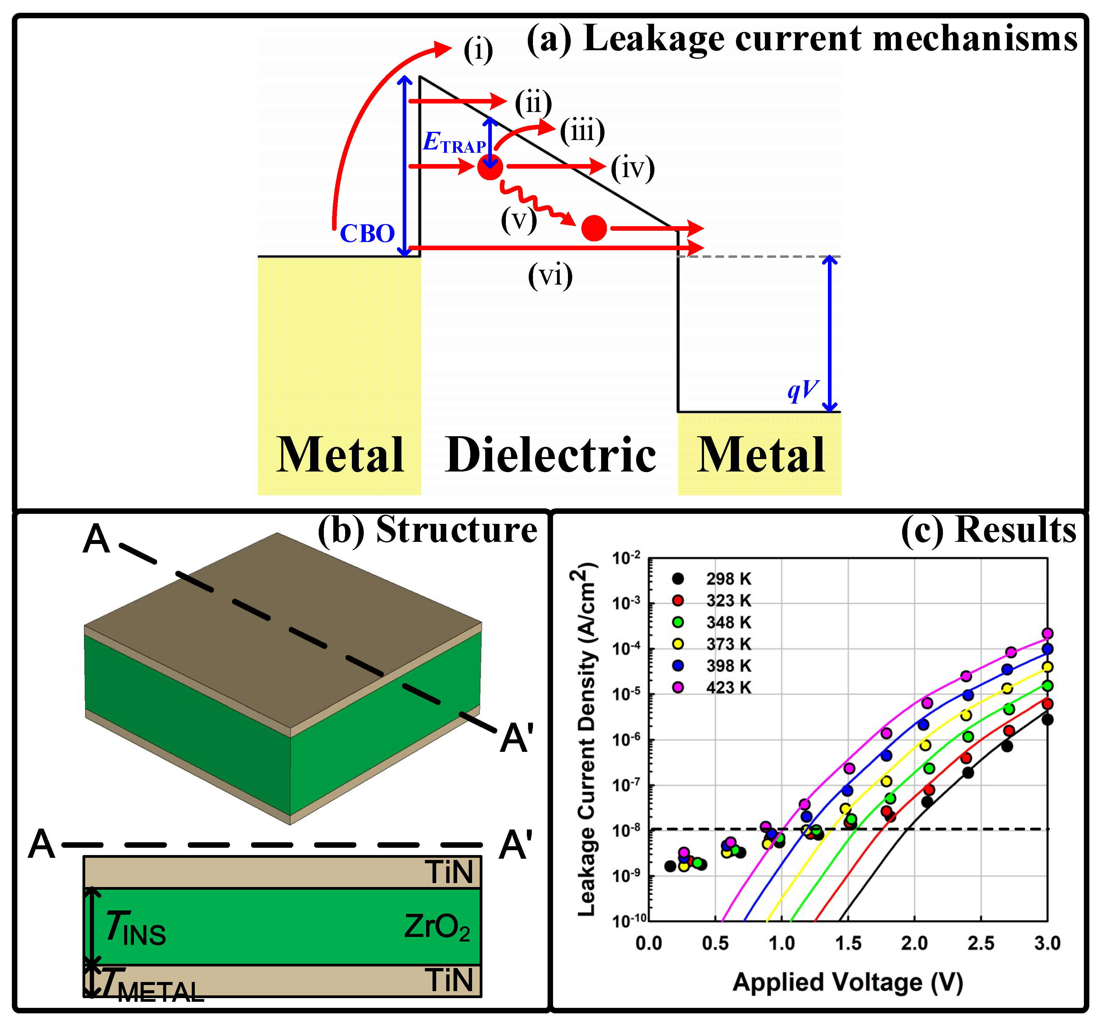
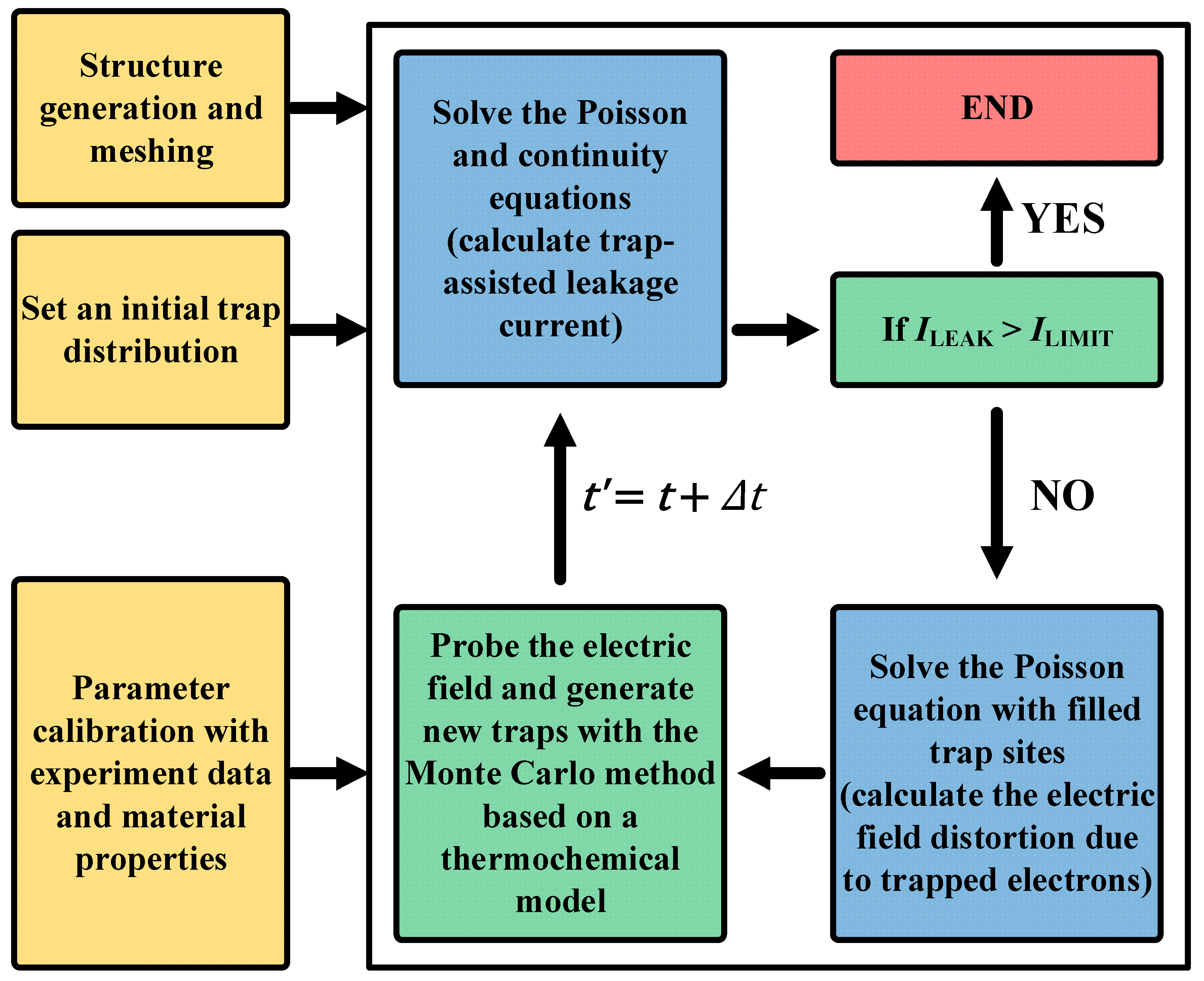
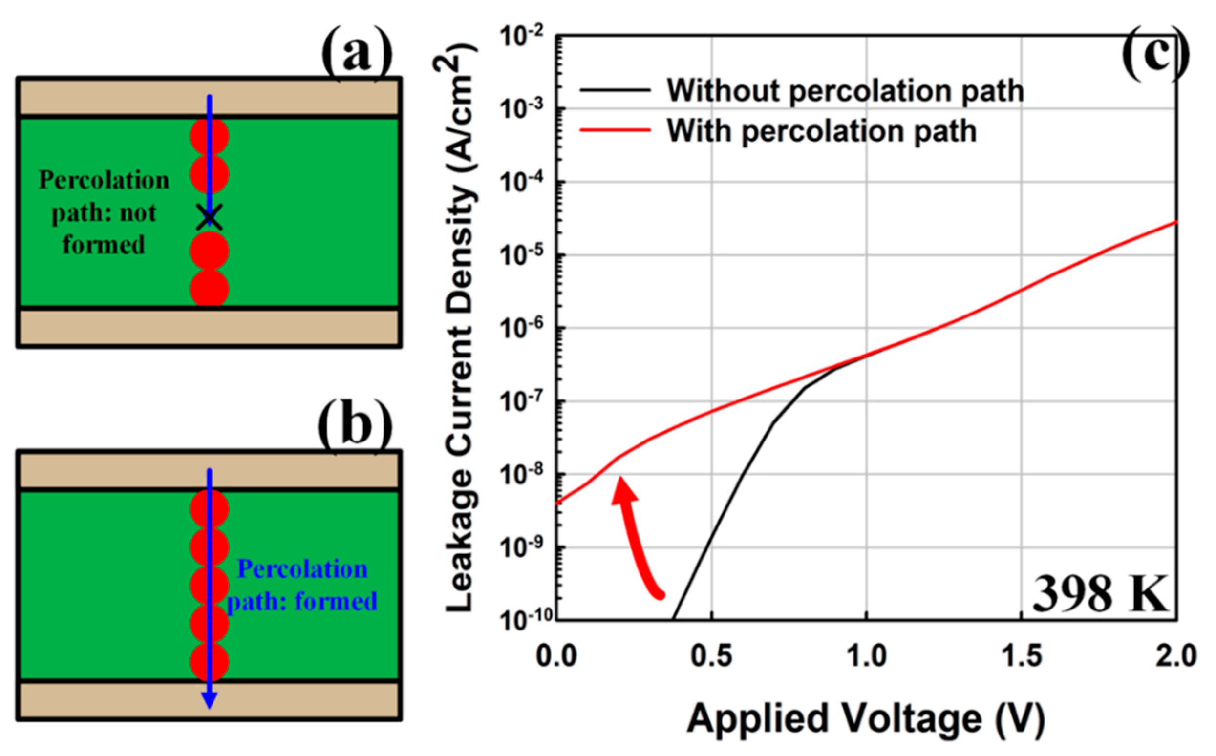
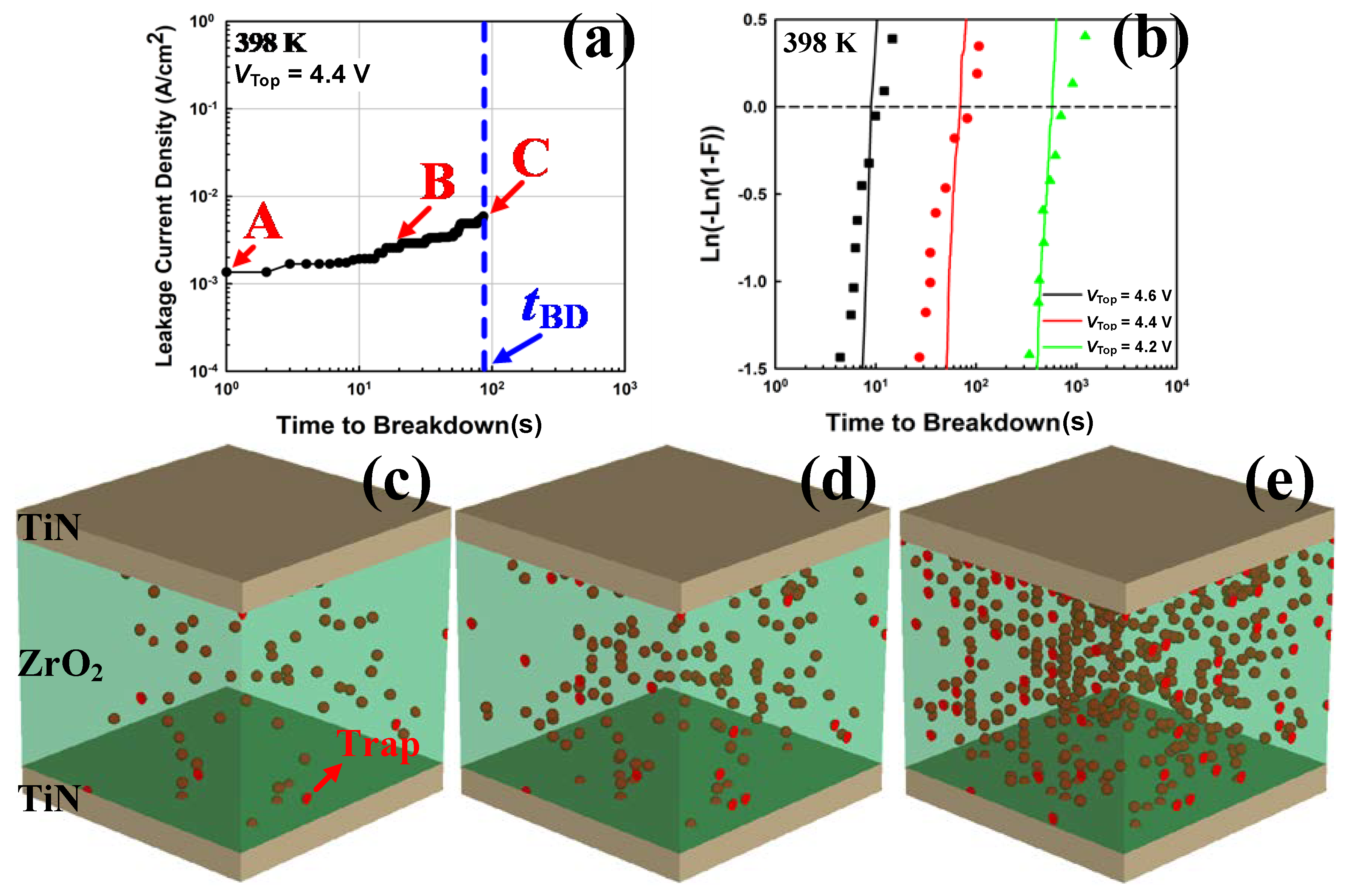
2. Methodology
3. Results and Discussion
4. Conclusions
Author Contributions
Funding
Conflicts of Interest
References
- Park, J.M.; Hwang, Y.S.; Kim, S.W.; Han, S.Y.; Park, J.S.; Kim, J.; Seo, J.W.; Kim, B.S.; Shin, S.H.; Cho, C.H.; et al. 20 nm DRAM: A new beginning of another revolution. In Proceedings of the 2015 IEEE International Electron Devices Meeting (IEDM), Washington, DC, USA, 7–9 December 2015. [Google Scholar]
- Park, S.-K. Technology Scaling Challenge and Future Prospects of DRAM and NAND Flash Memory. In Proceedings of the 2015 IEEE International Memory Workshop (IMW), Monterey, CA, USA, 17–20 May 2015; pp. 1–4. [Google Scholar]
- Kim, D.H.; Kim, J.Y.; Huh, M.; Hwang, Y.S.; Park, J.M.; Han, D.H.; Kim, D.I.; Cho, M.H.; Lee, B.H.; Hwang, H.K.; et al. A mechanically enhanced storage node for virtually unlimited height (MESH) capacitor aiming at sub 70 nm DRAMs. In Proceedings of the IEDM Technical Digest, IEEE International Electron Devices Meeting, San Francisco, CA, USA, 13–15 December 2004; pp. 69–72. [Google Scholar]
- Deok-Sin, K.; Song, H.-S.; Kee-Jeung, L.; Hong, K.; Jin-Hyock, K.; Park, K.-S.; Seung-Jin, Y.; Jae-Sung, R.; Noh-Jung, K.; Hyun-Chul, S.; et al. Development of New TiN/ZrO2/Al2O3/ZrO2/TiN Capacitors Extendable to 45 nm Generation DRAMs Replacing HfO2 Based Dielectrics. In Proceedings of the 2006 Symposium on VLSI Technology, 2006. Digest of Technical Papers, Honolulu, HI, USA, 13–15 June 2006; pp. 38–39. [Google Scholar]
- Padmanabhan, R.; Mohan, S.; Morozumi, Y.; Kaushal, S.; Bhat, N. Performance and Reliability of TiO2/ZrO2/TiO2 (TZT) and AlO-Doped TZT MIM Capacitors. IEEE Trans. Devices 2016, 63, 3928–3935. [Google Scholar] [CrossRef]
- Kaczer, B.; Larcher, L.; Vandelli, L.; Reisinger, H.; Popovici, M.; Clima, S.; Ji, Z.; Joshi, S.; Swerts, J.; Afanas’ev, V.V.; et al. SrTiOx for sub-20 nm DRAM technology nodes—Characterization and modeling. Microelectron. Eng. 2015, 147, 126–129. [Google Scholar] [CrossRef]
- Kittl, J.A. High-k dielectrics for future generation memory devices. Microelectron. Eng. 2009, 86, 1789–1795. [Google Scholar] [CrossRef]
- McPherson, J.; Kim, J.; Shanware, A.; Mogul, H.; Rodriguez, J. Trends in the ultimate breakdown strength of high dielectric-constant materials. IEEE Trans. Devices 2003, 50, 1771–1778. [Google Scholar] [CrossRef]
- Jegert, G.; Kersch, A.; Weinreich, W.; Lugli, P. Monte Carlo Simulation of Leakage Currents in TiN/ZrO2/TiN Capacitors. IEEE Trans. Electron Devices 2011, 58, 327–334. [Google Scholar] [CrossRef]
- Padovani, A.; Larcher, L. Time-dependent dielectric breakdown statistics in SiO2 and HfO2 dielectrics: Insights from a multi-scale modeling approach. In Proceedings of the 2018 IEEE International Reliability Physics Symposium (IRPS), Burlingame, CA, USA, 11–15 March 2018; p. 3A-2. [Google Scholar]
- Sentaurus Device Simulator. 2018. Available online: https//www.synopsys.com/silicon/tcad/device-simulation/sentaurus-device.html (accessed on 16 April 2019).
- Popescu, D.H. Modeling of Leakage Currents in High-k Dielectrics for Future DRAM Application. Doctoral Dissertation, Technische Universität München, Munich, Germany, 2015. [Google Scholar]
- Weinreich, W.; Shariq, A.; Seidel, K.; Sundqvist, J.; Paskaleva, A.; Lemberger, M.; Bauer, A.J. Detailed leakage current analysis of metal–insulator–metal capacitors with ZrO2, ZrO2/SiO2/ZrO2, and ZrO2/Al2O3/ZrO2 as dielectric and TiN electrodes. J. Vac. Sci. Technol. B 2013, 31, 1. [Google Scholar] [CrossRef]
- Jegert, G.; Kersch, A.; Weinreich, W.; Schröder, U.; Lugli, P. Modeling of leakage currents in high-κ dielectrics: Three-dimensional approach via kinetic Monte Carlo. Appl. Phys. Lett. 2010, 96, 62113. [Google Scholar] [CrossRef]
- Palma, A.; Godoy, A.; Carceller, J.E.; Villanueva, J.A.L.; Jimenez-Tejada, J.A. Quantum two-dimensional calculation of time constants of random telegraph signals in metal-oxide–semiconductor structures. Phys. Rev. B 1997, 56, 9565–9574. [Google Scholar] [CrossRef]
- Cartujo, P.; Jiménez-Molinos, F.; Gámiz, F.; Villanueva, J.A.L.; Palma, A. Direct and trap-assisted elastic tunneling through ultrathin gate oxides. J. Appl. Phys. 2002, 91, 5116–5124. [Google Scholar]
- Nasyrov, K.A.; Gritsenko, V. Charge transport in dielectrics via tunneling between traps. J. Appl. Phys. 2011, 109, 93705. [Google Scholar] [CrossRef]
- Colalongo, L.; Valdinoci, M.; Baccarani, G.; Migliorato, P.; Tallarida, G.; Reita, C. Numerical analysis of poly-TFTs under off conditions. Solid-State Electron. 1997, 41, 627–633. [Google Scholar] [CrossRef]
- Pešić, M.; Knebel, S.; Geyer, M.; Schmelzer, S.; Böttger, U.; Kolomiiets, N.; Afanas’ev, V.V.; Cho, K.; Jung, C.; Chang, J.; et al. Low leakage ZrO2 based capacitors for sub 20 nm dynamic random access memory technology nodes. J. Appl. Phys. 2016, 119, 064101. [Google Scholar] [CrossRef]
- Jegert, G.; Popescu, D.; Lugli, P.; Häufel, M.J.; Weinreich, W.; Kersch, A. Role of defect relaxation for trap-assisted tunneling in high-κ thin films: A first-principles kinetic Monte Carlo study. Phys. Rev. B 2012, 85, 045303. [Google Scholar] [CrossRef]
- Kwon, H.-M.; Kwon, S.-K.; Jeong, K.-S.; Oh, S.-K.; Oh, S.-H.; Choi, W.-I.; Kim, T.-W.; Kim, D.-H.; Kang, C.-Y.; Lee, B.H.; et al. A Correlation between Oxygen Vacancies and Reliability Characteristics in a Single Zirconium Oxide Metal-Insulator-Metal Capacitor. IEEE Trans. Devices 2014, 61, 2619–2627. [Google Scholar] [CrossRef]
- Gao, D.Z.; Strand, J.; El-Sayed, A.-M.; Shluger, A.L.; Padovani, A.; Larcher, L. Role of electron and hole trapping in the degradation and breakdown of SiO2 and HfO2 films. In Proceedings of the 2018 IEEE International Reliability Physics Symposium (IRPS), Burlingame, CA, USA, 11–15 March 2018; p. 5A-2. [Google Scholar]
- Jackson, J.D. Classical Electrodynamics; John Wiley & Sons: Hoboken, NJ, USA, 2007. [Google Scholar]
- Bhattacharya, K. On the dependence of charge density on surface curvature of an isolated conductor. Phys. Scr. 2016, 91, 35501. [Google Scholar] [CrossRef] [Green Version]


© 2019 by the authors. Licensee MDPI, Basel, Switzerland. This article is an open access article distributed under the terms and conditions of the Creative Commons Attribution (CC BY) license (http://creativecommons.org/licenses/by/4.0/).
Share and Cite
Choi, W.Y.; Yoon, G.; Chung, W.Y.; Cho, Y.; Shin, S.; Ahn, K.H. A Technology-Computer-Aided-Design-Based Reliability Prediction Model for DRAM Storage Capacitors. Micromachines 2019, 10, 256. https://doi.org/10.3390/mi10040256
Choi WY, Yoon G, Chung WY, Cho Y, Shin S, Ahn KH. A Technology-Computer-Aided-Design-Based Reliability Prediction Model for DRAM Storage Capacitors. Micromachines. 2019; 10(4):256. https://doi.org/10.3390/mi10040256
Chicago/Turabian StyleChoi, Woo Young, Gyuhan Yoon, Woo Young Chung, Younghoon Cho, Seongun Shin, and Kwang Ho Ahn. 2019. "A Technology-Computer-Aided-Design-Based Reliability Prediction Model for DRAM Storage Capacitors" Micromachines 10, no. 4: 256. https://doi.org/10.3390/mi10040256