A Novel Three-Axial Magnetic-Piezoelectric MEMS AC Magnetic Field Sensor


Abstract
:1. Introduction
2. Design
2.1. Sensor Design
2.2. Background Theories of Magnetic Force and Piezoelectric Voltage Output
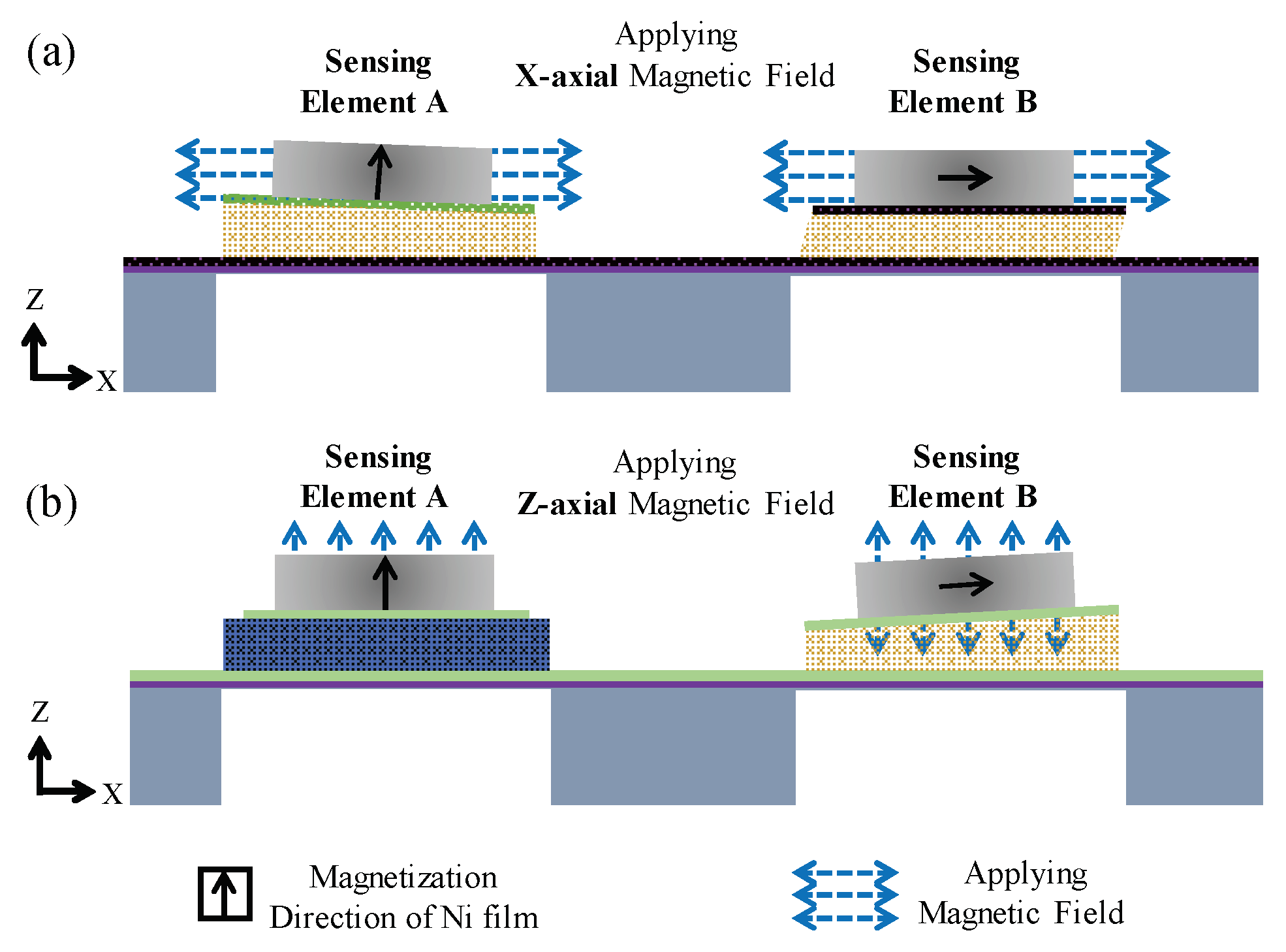
2.3. Magnetic Field Sensing Principle
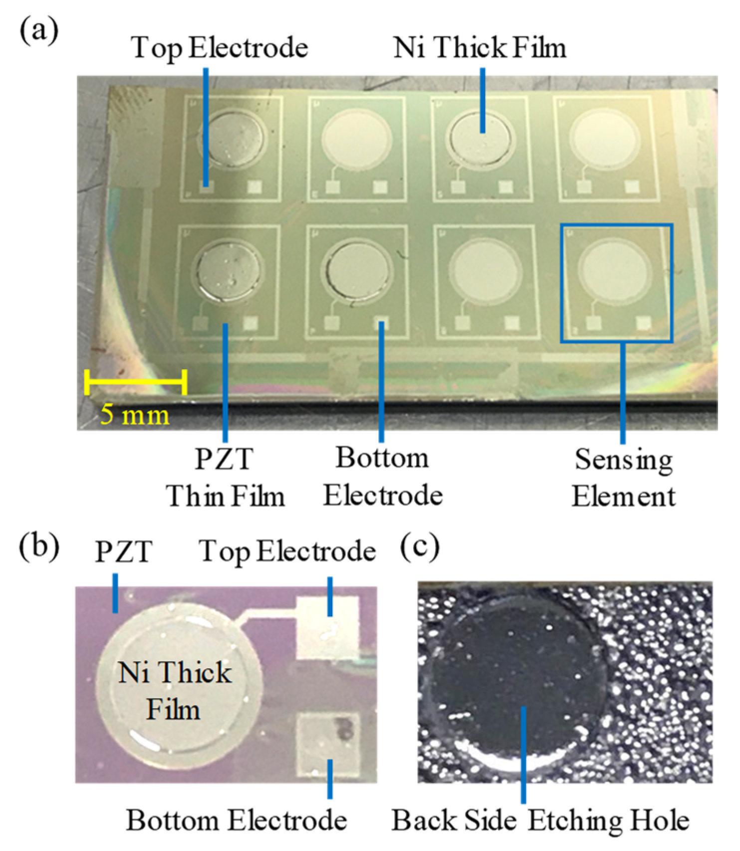
3. Fabrication
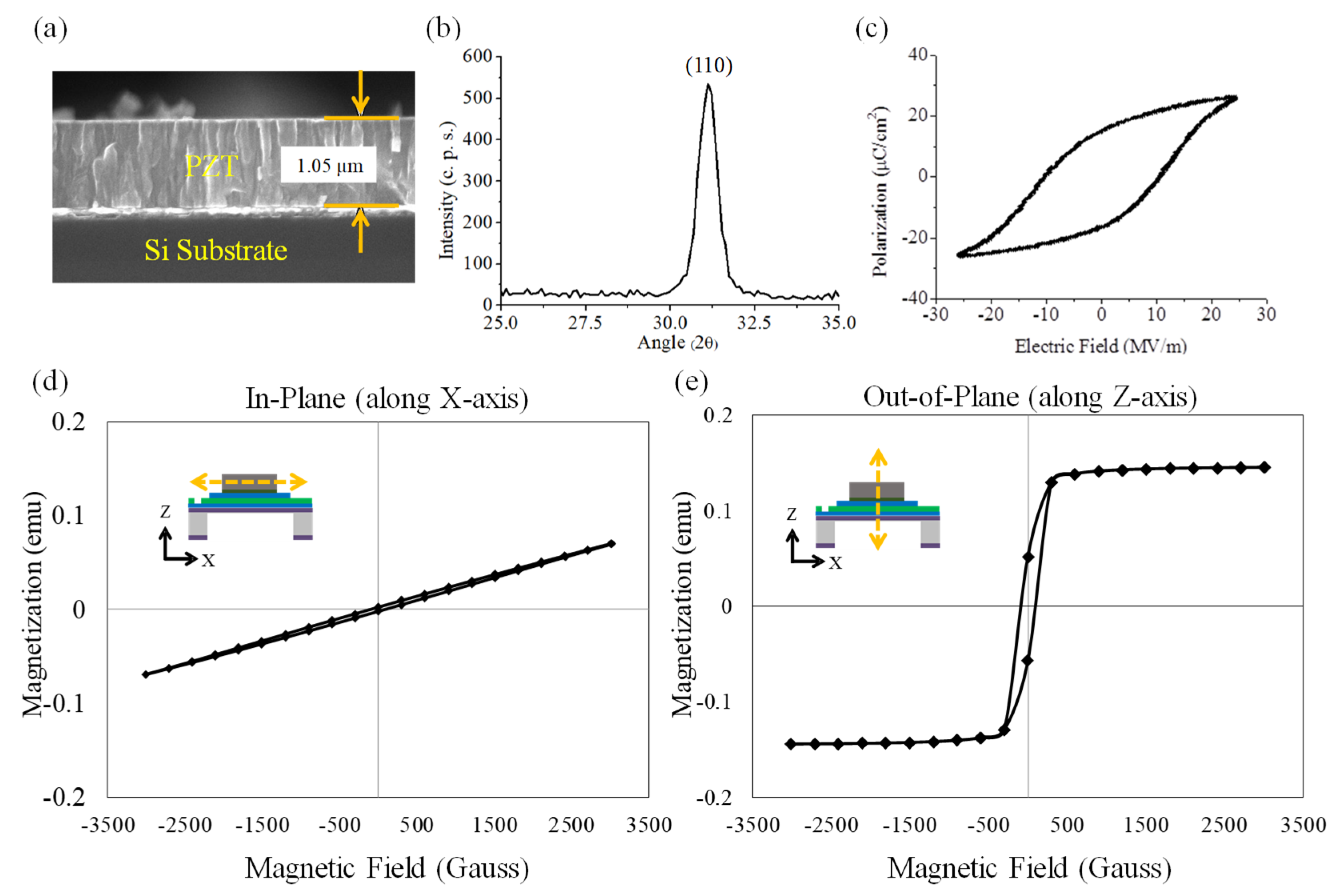
4. Characterization
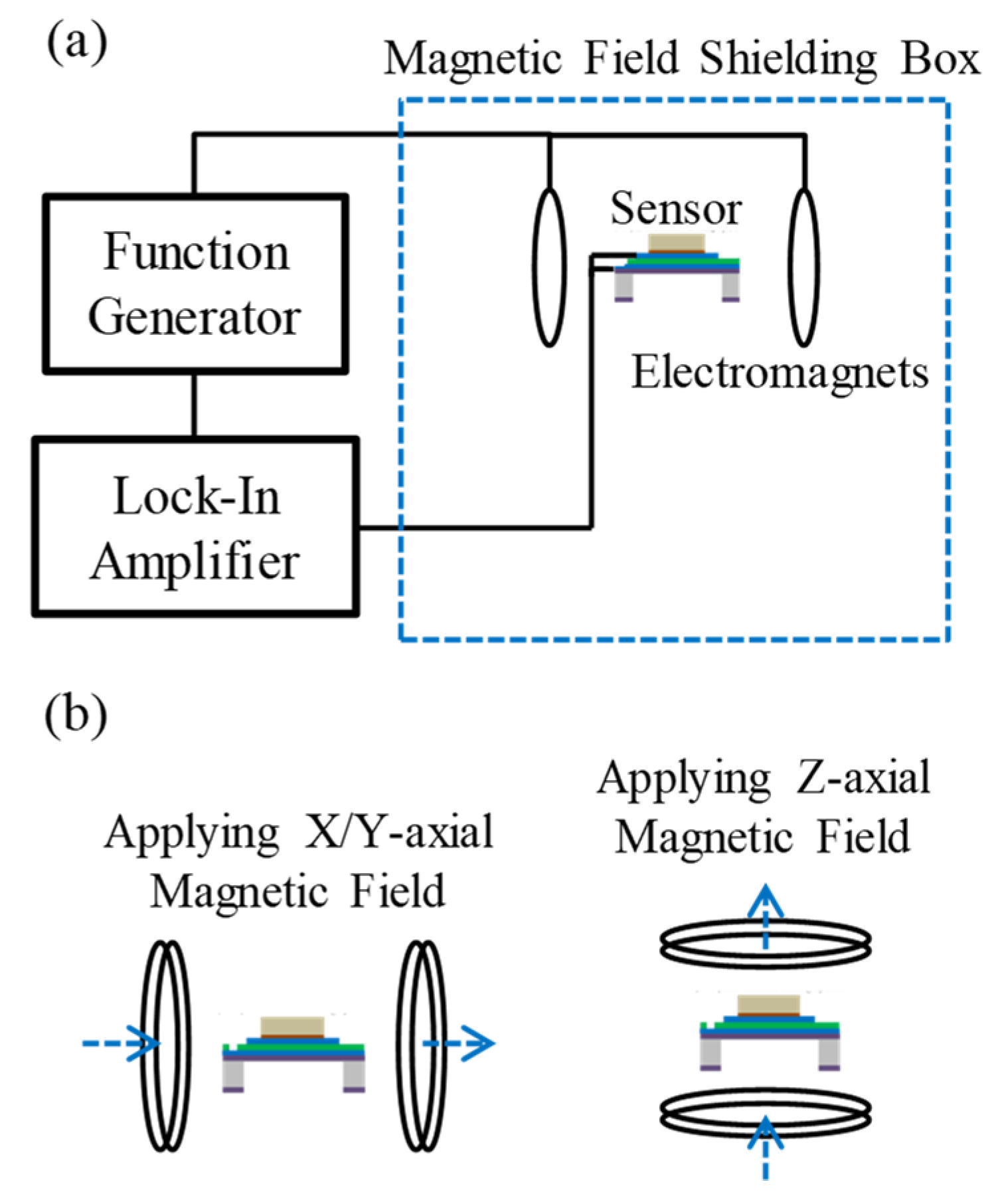
5. Testing
6. Results and Discussions
7. Conclusions
Supplementary Materials
Author Contributions
Funding
Conflicts of Interest
References
- Ripka, P. Magnetic sensors and magnetometers. Meas. Sci. Technol. 2002, 13, 645. [Google Scholar] [CrossRef]
- Vopalensky, M.; Ripka, P.; Platil, A. Precise magnetic sensors. Sens. Actuators A 2003, 106, 38–42. [Google Scholar] [CrossRef]
- Ripka, P. Advances in magnetic field sensors. IEEE Sens. J. 2010, 10, 1108–1116. [Google Scholar] [CrossRef]
- Lenz, J.; Edelstein, S. Magnetic sensors and their applications. IEEE Sens. J. 2006, 6, 631–649. [Google Scholar] [CrossRef]
- Yeh, P.C.; Chung, T.K.; Lai, C.H.; Wang, C.M. A magnetic-piezoelectric smart material-structure utilizing magnetic-force-interaction to optimize the sensitivity of current sensing. Appl. Phys.-A 2016, 122, 83–90. [Google Scholar] [CrossRef]
- Hung, C.F.; Chen, C.C.; Yeh, P.C.; Chen, P.W.; Chung, T.K. A magnetic-piezoelectric smart material-structure sensing three axis DC and AC magnetic-fields. Appl. Phys.-A 2017, 123, 739. [Google Scholar] [CrossRef]
- Hung, C.F.; Chen, C.C.; Yeh, P.C.; Chung, T.K. A miniature magnetic-force-based three-axis AC magnetic sensor with piezoelectric/vibrational energy-harvesting functions. Sensors 2017, 17, 308. [Google Scholar] [CrossRef]
- Hung, C.F.; Chung, T.K.; Yeh, P.C.; Chen, C.C.; Wang, C.M.; Lin, S.H. A miniature mechanical-piezoelectric-configured three-axis vibrational energy harvester. IEEE Sens. J. 2015, 15, 5601–5615. [Google Scholar] [CrossRef]
- Chen, J.; Li, J.; Xu, L. Highly integrated MEMS magnetic sensor based on GMI effect of amorphous wire. Micromachines 2019, 10, 237. [Google Scholar] [CrossRef]
- Lin, Y.N.; Dai, C.L. Micro magnetic field sensors manufactured using a standard 0.18-µm CMOS process. Micromachines 2018, 9, 393. [Google Scholar] [CrossRef]
- Nakai, T. Magneto-impedance sensor driven by 400 MHz logarithmic amplifier. Micromachines 2019, 10, 355. [Google Scholar] [CrossRef] [PubMed]
- Yang, X.; Zhao, X.; Bai, Y.; Lv, M.; Wen, D. Two-demensional magnetic field sensor based on silicon magnetic sensitive transistors with differential structure. Micromachines 2017, 8, 95. [Google Scholar] [CrossRef]
- Hall Effect Sensing and Applications, Honeywell. Available online: https://sensing.honeywell.com/hallbook.pdf (accessed on 1 August 2019).
- Magnetic Displacement Sensors HMC1501/1512, Honeywell. Available online: https://datasheet.octopart.com/HMC1512-Honeywell-datasheet-15910273.pdf (accessed on 1 August 2019).
- Rouf, V.T.; Li, M.; Horsley, D.A. Area-efficient three axis MEMS Lorentz force magnetometer. IEEE Sens. J. 2013, 13, 4474–4481. [Google Scholar] [CrossRef]
- Wu, L.; Tian, Z.; Ren, D.; You, Z. A miniature resonant and torsional magnetometer based on Lorentz force. Micromachines 2018, 9, 666. [Google Scholar] [CrossRef] [PubMed]
- Ettelt, D.; Rey, P.; Jourdan, G.; Walther, A.; Robert, P.; Delamare, J. 3D magnetic field sensor concept for use in inertial measurement units (IMUs). J. MEMS 2014, 23, 324–333. [Google Scholar] [CrossRef]
- Marauska, S.; Jahns, R.; Kirchhof, C.; Claus, M.; Quandt, E.; Knöchel, R.; Wagner, B. Highly sensitive wafer-level packaged MEMS magnetic field sensor based on magnetoelectric composites. Sens. Actuators A 2013, 189, 321–327. [Google Scholar] [CrossRef]
- Nan, T.; Hui, Y.; Rinaldi, M.; Sun, N.X. Self-biased 215MHz magnetoelectric NEMS resonator for ultra-sensitive DC magnetic field detection. Sci. Rep. 2013, 3, 1985. [Google Scholar] [CrossRef]
- Laletin, U.; Sreenivasulu, G.; Petrov, V.M.; Garg, T.; Kulkarni, A.R.; Venkataramani, N.; Srinivasan, G. Hysteresis and remanence in magnetoelectric effects in functionally graded magnetostrictive-piezoelectric layered composites. Phys. Rev. B 2012, 85, 104404. [Google Scholar] [CrossRef]
- Lage, E.; Urs, N.O.; Röbisch, V.; Teliban, I.; Knöchel, R.; Meyners, D.; McCord, J.; Quandt, E. Magnetic domain control and voltage response of exchange biased magnetoelectric composites. Appl. Phys. Lett. 2014, 104, 132405. [Google Scholar] [CrossRef]
- Zhang, J.; Li, P.; Wen, Y.; He, W.; Yang, A.; Lu, C. Giant self-biased magnetoelectric response with obvious hysteresis in layered homogeneous composites of negative magnetostrictive material Samfenol and piezoelectric ceramics. Appl. Phys. Lett. 2013, 103, 202902. [Google Scholar] [CrossRef]
- Tong, B.; Yang, X.; Ouyang, J.; Lin, G.; Zhang, Y.; Chen, S. Magnetoelectric response of AlN/[(Fe90Co10)78Si12B10 + Terfenol-D] composite films. Appl. Phys. Lett. 2014, 115, 17D904. [Google Scholar] [CrossRef]
- Shen, Y.; Gao, J.; Wang, Y.; Li, J.; Viehland, D. High non-linear magnetoelectric coefficient in Metglas/PMN-PT laminate composites under zero direct current magnetic bias. Appl. Phys. Lett. 2014, 115, 094102. [Google Scholar] [CrossRef] [Green Version]
- Cui, N.; Wu, W.; Zhao, Y.; Bai, S.; Meng, L.; Qin, Y.; Wang, Z.L. Magnetic force driven nanogenerators as a noncontact energy harvester and sensor. Nano Lett. 2002, 12, 3701–3705. [Google Scholar] [CrossRef] [PubMed]
- Yeh, P.C.; Dun, H.; Chung, T.K. A novel self-powered piezoelectric three-axis MEMS magnetic sensor. In Proceedings of the 19th International Conference on Slid-State Sensors, Actuators and Microsystems (Transducers 2017), Kaohsiung, Taiwan, 18–22 June 2017. [Google Scholar] [CrossRef]
- Yeh, P.C.; Dun, H.; Chung, T.K. Three-axis MEMS DC magnetic sensor using magnetic force interaction with the piezoelectric effect. In Proceedings of the 17th International Conference on Micro and Nanotechnology for Power Generation and Energy Conversion Applications (PowerMEMS 2017), Kanasawa, Japan, 14–17 November 2017. [Google Scholar] [CrossRef]
- Chen, C.C.; Chen, I.L.; Duan, H.; Tseng, C.Y.; Chung, T.K. A thermomagnetic-piezoelectric MEMS AC magnetic-field sensor demonstrating a novel room-temperature-range coil-less resetting/demagnetizing approach, Sensors and amp. Sens. Actuators A 2019. [Google Scholar] [CrossRef]
- Shih, V.; Cheng, S.; Lin, Y.R.; Lin, A.; Liao, Y.J.; Lin, C.H.; Huang, F.C.; Tai, K.; Hu, F.; Tsai, Y.H.; et al. Highly reliable piezoelectric process technology in volume foundry for emerging MEMS applications. In Proceedings of the 20th International Conference on Solid-State Sensors, Actuators and Microsystems & Eurosensors XXXIII (TRANSDUCERS & EUROSENSORS XXXIII), T1E003, Berlin, Germany, 23–27 June 2019. [Google Scholar]
- Vokoun, D.; Beleggia, M.; Heller, L.; Sittner, P. Magnetostatic interactions and forces between cylindrical permanent magnets. J. Magn. Magn. Mater. 2009, 321, 3758–3763. [Google Scholar] [CrossRef]
- Roundy, S.; Wright, P.K. A piezoelectric vibration based generator for wireless electronics. Smart Mater. Struct. 2004, 13, 1131–1142. [Google Scholar] [CrossRef] [Green Version]
- Chung, T.K.; Carman, G.P.; Mohanchandra, K.P. Reversible magnetic domain-wall motion under an electric field in a magnetoelectric thin film. Appl. Phys. Lett. 2008, 92, 112509. [Google Scholar] [CrossRef]
- Chung, T.K.; Wang, H.M.; Chen, Y.J.; Lin, S.H.; Chu, H.J.; Lin, P.J.; Hung, C.F. Magnetic-field-assisted electric-field-controlled rotation of magnetic stripe domains in a magnetoelectric Ni microbar/[Pb(Mg1/3Nb2/3)O3]0.68–[PbTiO3]0.32 heterostructure. Appl. Phys. Express 2016, 9, 043003. [Google Scholar] [CrossRef]


| Working Mechanism | Schematic Diagram of αME-H Curve | Representative Works | ME Composites | HOPT (Oe) | ME Coupling | |
|---|---|---|---|---|---|---|
| α ME @ HOPT (V cm−1 Oe−1) | fAC (kHz) | |||||
| Functionally Graded |  | Laletin et al. 2012 [20] | PZT/Ni/NZFO | 0 | 0.28 | 0.02 |
| Exchange Bias Mediated |  | Lage et al. 2014 [21] | Fe50Co50/AlN | 0 | 96.7 | 1.19 |
| Magnetostriction Hysteresis Based |  | Zhang et al. 2013 [22] | SmFe2/PZT | 272 | 39.5 | 119.7 |
| Build-In Stress Mediated |  | Tong et al. 2014 [23] | FeCoSiB/Terfenol/AlN | 11 | 78.1 | 1 |
| Non-linear |  | Shen et al. 2014 [24] | Metglas/PMN-PT | 0 | 100 | 24.2 |
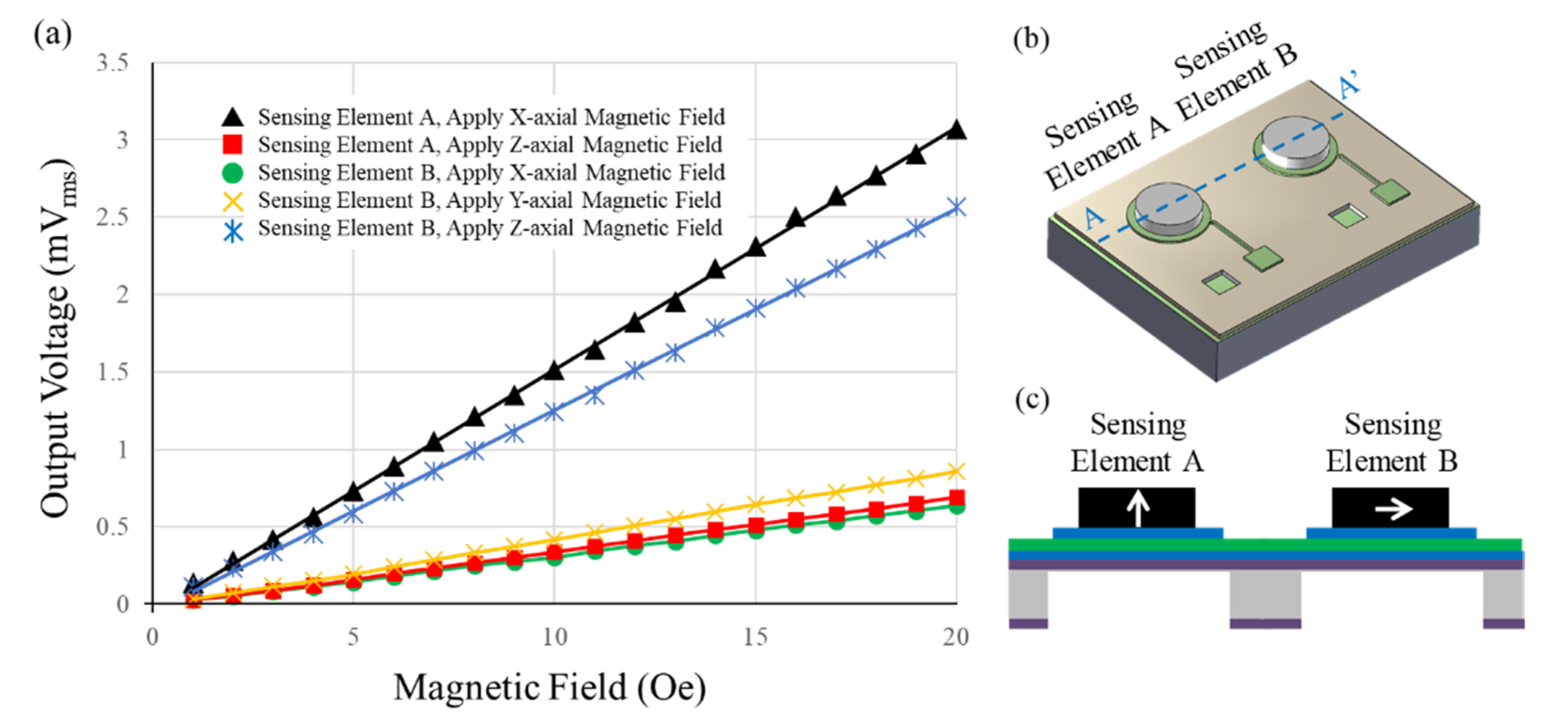
| Applied Magnetic Field | Sensing Element A Magnetization-Direction: Z axis | Sensing Element B Magnetization-Direction: X axis |
|---|---|---|
| X-axial | 0.156 mVrms/Oe | 0.033 mVrms/Oe |
| Y-axial | 0.044 mVrms/Oe | |
| Z-axial | 0.035 mVrms/Oe | 0.130 mVrms/Oe |
© 2019 by the authors. Licensee MDPI, Basel, Switzerland. This article is an open access article distributed under the terms and conditions of the Creative Commons Attribution (CC BY) license (http://creativecommons.org/licenses/by/4.0/).
Share and Cite
Yeh, P.-C.; Duan, H.; Chung, T.-K. A Novel Three-Axial Magnetic-Piezoelectric MEMS AC Magnetic Field Sensor. Micromachines 2019, 10, 710. https://doi.org/10.3390/mi10100710
Yeh P-C, Duan H, Chung T-K. A Novel Three-Axial Magnetic-Piezoelectric MEMS AC Magnetic Field Sensor. Micromachines. 2019; 10(10):710. https://doi.org/10.3390/mi10100710
Chicago/Turabian StyleYeh, Po-Chen, Hao Duan, and Tien-Kan Chung. 2019. "A Novel Three-Axial Magnetic-Piezoelectric MEMS AC Magnetic Field Sensor" Micromachines 10, no. 10: 710. https://doi.org/10.3390/mi10100710