Article

A Study and Implementation of Inductive Power Transfer System Using Hybrid Control Strategy for CC-CV Battery Charging

1
Department of Electrical and Electronic Engineering, The University of Hong Kong, Hong Kong 999077, China
2
College of Electrical Engineering, Zhejiang University, Hangzhou 310058, China
*
Author to whom correspondence should be addressed.
Sustainability 2023, 15(4), 3606; https://doi.org/10.3390/su15043606
Submission received: 16 January 2023 / Revised: 6 February 2023 / Accepted: 10 February 2023 / Published: 15 February 2023

Abstract

:
In this paper, a hybrid control strategy is studied and implemented on an Inductive Power Transfer (IPT) system to simultaneously realize zero-voltage switching (ZVS) and constant current (CC) and constant voltage (CV) battery charging. A steady-state analysis of pulse frequency modulation was conducted, based on the characteristic of voltage gain versus switching frequency, and CC and CV charging modes were promised. The ZVS of the inverter was obtained by satisfying the minimum requirement of full discharge of the junction capacitor on the MOSFETs using a commutation current during the dead-time interval. Two control degrees of freedom are needed to realize the two control targets. This hybrid control strategy adopts a self-oscillating (SO) control to achieve ZVS and phase shift (PS) control and a constant output for the series–series (SS)-compensated IPT system. To validate the hybrid control strategy, a 1.6 kW prototype with 360–440 V input voltage and 250–400 V output voltage was built and the experimental results show that the peak efficiency can reach 96.1%. Compared with the conventional variable frequency (VF) control, the hybrid control method proves that an additional control variable can fulfill the control target in a more flexible manner, which makes the switching frequency close to the resonant frequency during the charging process, minimizing the reactive current in the resonant tank and improving system efficiency.

1. Introduction

Inductive power transfer (IPT) has attracted attention in recent years because of its high reliability, safety, and convenience. It has been utilized in numerous applications, such as medical implantable pacemakers, portable electronic devices, electric vehicles (EVs), and railway transportation. EVs not only consume renewable energy but also act as a movable power supply. IPT facilitates convenient interactions between EVs and power grids. The IPT technology used for battery charging in EVs is one of the most promising applications, and the employment of IPT will considerably alleviate range anxiety. Therefore, the IPT battery-charging technique is of great importance in the development of the EVs in the future [1,2,3,4,5,6,7,8,9,10,11,12,13,14].
In order to prevent degradation of battery life and improve the efficiency of the charging system, some key issues remain to be addressed. For practical applications, a constant current (CC) and constant voltage (CV) are always essential in the charging profile, as the equivalent resistance of battery varies dynamically during the charging process [7]. Besides, it is crucial to minimize the reactive current within the charging process on the premise of a zero-voltage switching (ZVS) operation [15,16], where ZVS can lead to reduced switching loss and eliminate some of the sources of converter-generated electro-magnetic interference (EMI) [17].
According to a literature review, the variable compensation topology has been widely utilized in battery-charging systems [18,19,20] and its basic principle involves changing the resonant tank by using additional switches to implement a CC- and CV-mode charge operation. As a result, the IPT battery-charging system can achieve a zero phase angle (ZPA) operation and thereby reduce the reactive current. The adoption of additional switches should be circumvented to the utmost as it may degrade the system efficiency. In [21,22], double-sided LCC-compensated IPT charging systems are presented to realize load-independent CC and CV outputs at two different switching frequencies.
The control strategy is an acceptable alternative to fulfill the charging profile using simple compensation topologies. They can be roughly categorized as pulse width modulation (PWM), pulse density modulation (PDM), phase shift (PS), variable frequency (VF), and self-oscillation (SO), etc. [23,24,25,26,27]. In [23], PS control is adopted to realize a constant current or voltage output, but it has a serious deficiency: ZVS cannot be achieved throughout the whole charging process. In [24], VF control is employed to regulate the output voltage with ZVS for a series–series (SS)-compensated IPT system. Aside from the high reactive current and component stresses caused by the switching frequency’s deviation from the resonant frequency, frequency bifurcation may occur when multiple frequencies can satisfy ZVS operation, resulting in system instability. In [25], a PDM ZVS full bridge converter for an IPT system is proposed to eliminate the dependence on coupling and load conditions, but this needs an LC branch to provide the ZVS current, resulting in additional power losses. In [26,27], SO control is presented for an SS-compensated IPT converter. They mainly focus on the frequency tuning and dynamic response instead of the regulation of output power.
At least two control degrees of freedom are needed to simultaneously realize the two control targets, i.e., the constant output and ZVS. Therefore, the other potential solutions to the above-mentioned issues fall on hybrid control strategies. In [28], the combination of PWM and phase-locked loop (PLL) is proposed to realize a constant output voltage and ZVS operation. A new SO-tuning loop for IPT systems with PS and PWM control is proposed, while the characteristics of battery charging are not investigated [29]. In [30,31], VF and PS hybrid control strategies are presented for battery-charging systems. Hybrid control may suffer from hard switching, especially under light load conditions [32]. In [33], a coordination control of PS and an auxiliary variable inductor (VI) installed in the primary side are proposed to achieve stable output and extend the ZVS operation range. In [34], a dynamic tuning method of ZVS angle using a variable capacitor is proposed, and PS is implemented to achieve a constant output. In [35], it is proven that hybrid controllers can serve a lot better than standalone controllers in precise control applications.
A hybrid control strategy for CC-CV battery charging and ZVS tracking is studied and implemented in this paper. The main contributions of this paper are summarized as follows.
The analysis of a series–series (SS)-compensated IPT system is conducted, looking at the control target, steady-state analysis of pulse frequency modulation, ZVS tracking, and limits on the degree of freedom for VF control. During implementation, using the characteristics of the voltage gains versus switching frequency, the CC- and CV-charging modes can be achieved. Meanwhile, ZVS tracking is analyzed in detail. This reveals that the minimum requirement to realize ZVS is to discharge the junction capacitor on the MOSFETs, which is highly related to the drain-source voltage, dead-time interval, and commutation current. Two types of control strategies, i.e., VF and SO-PS, are discussed. This shows that the VF control strategy will be further from the natural resonant frequency, while the adoption of an additional control variable phase shift helps to complete the same control target in a more flexible way.
The rest of the paper is organized as follows. Section 2 details the steady-state characteristic of the SS-compensated IPT system. In Section 3, the implementation of a hybrid control strategy is presented. In Section 4, an experimental prototype with 360–440 V input voltage and 250–400 V output voltage is built to verify the hybrid control strategy. Finally, the conclusion is given in Section 5.

2. Analysis of SS-Compensated IPT System

Figure 1 shows the circuit architecture of the SS-compensated IPT charging system. The high-frequency inverter has a full bridge consisting of four power MOSFETs (S1-S4). Vin and vp denote the DC and AC voltages of the inverter, respectively. The rectifier comprises four diodes (D1–D4) and a filter capacitor Co. vs is the output voltage before the rectifier. Vo and Io are the output voltage and current of the IPT charging system. Lp and Ls are the self-inductance of the primary and secondary coils. M is the mutual inductance between two coils, and the coupling coefficient is k = M/(LpLs)1/2. Cp and Cs are resonant capacitors that are used to compensate Lp and Ls.
For simplicity, the resonant frequency between the primary side and secondary side are set to be equal, which satisfies:
ω r = 1 L p C p = 1 L s C s
The transferred power of the IPT system is mainly related to the fundamental component while the high-order harmonics contribute little to the power transfer. To simplify the analysis, the fundamental harmonic approximation (FHA) is used. The ac equivalent circuit model is shown in Figure 2. ω denotes the switching angular frequency.
The fundamental component of vp is derived as:
v p = 2 2 π V in
According to Kirchhoff’s law, the ac equivalent circuit can be expressed by:
v p = j ω L p 1 ω C p i p j ω M i s v s = j ω M i p j ω L s 1 ω C s i s

2.1. System Specifications

In general, Li-ion battery cells are commonly used for high-voltage battery packs. As indicated, the cell voltage exhibits a wide voltage range (1–4.2 V) throughout the whole charging process. In this paper, the voltage range of the battery pack is 250–400 V. The maximum charging current of the battery pack is 4 A. Figure 3 illustrates a simplified battery charging profile. There are two sequential processes: CC mode and CV mode.
From Figure 3, the battery pack appears to the IPT charger as a variable equivalent resistance RL, which is defined as the ratio of charging voltage to current. During the CC mode (between the time interval t0 and t1), the corresponding equivalent resistance of the battery packs increased from RA (62.5 Ω) to RB (100 Ω). In the CV mode, the charging current will decrease, and the maximum equivalent resistance is RC (800 Ω).
It should be noted that the nominal input voltage of the IPT charger from the front-end AC/DC converter varies between 360 V and 440 V (400 V ± 10%). Table 1 shows the electrical specification of the IPT charging system.

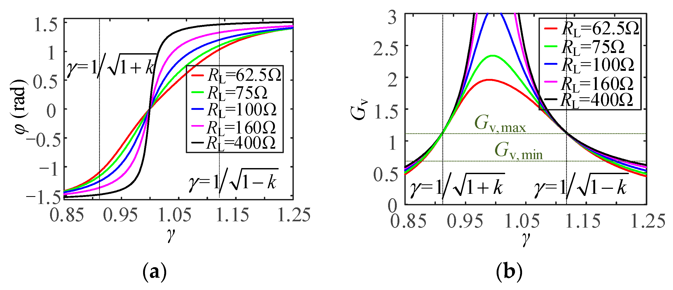
2.2. Steady-State Analysis of Pulse Frequency Modulation

Normalized parameters help to find the transfer function of the IPT system. These equations are defined and explained as follows:
α = L p L s γ = ω ω r X Ls = ω r L s Q = π 2 X Ls 8 R L
where α is the inductance ratio of transmitter coil over receiver coil, γ is the normalized switching frequency in terms of primary natural resonant frequency ωr = 1/ L p C p , XLs stands for the impedance of Ls and Q stands for the load quality factor.
From (3), the current of transmitter coil can be derived as
i p = v p α X Ls j γ γ 2 1 Q + γ 2 γ 4 k 2 Q γ 2 1 2 Q + j γ γ 2 1
Hence, the steady-state voltage gain Gv can be expressed as
G v = j γ 3 k α γ 4 k 2 α Q γ 2 1 2 α Q + j γ γ 2 1 α
According to Figure 2, the input impedance angle φ can be calculated as
φ = arctan γ γ 2 1 1 Q + γ 2 1 2 Q γ 3 k 2 γ 2 1 Q γ 4 k 2
It is well-known that an SS-compensation topology can achieve both CC output and CV output. To achieve the CC output, the system should be operated at the natural resonance frequency, and the following equation should be satisfied according to Equation (6).
γ γ 2 1 α = 0     γ = 1
When Equation (8) is satisfied, the voltage gain Gv is inversely proportional to the load quality factor, which means that only CC output is achieved. However, the following stage CV output is hard to realize because the system does not have a good voltage regulation ability unless an additional converter is adopted [36]. Considering the specification listed in Table 1, there are some constraints when the SS-compensated IPT converter operates at the CC output condition, i.e., γ = 1. Several preliminary limitations can be drawn as follows:
(1)
The inductance of the primary and secondary coil must be quite large to achieve the desired mutual inductance M. For instance, the output current at γ = 1 is approximately inversely proportional to M, i.e., Io = Vin/(ωM). Assuming that the operating frequency is 85 kHz and k = 0.2, M = 187 μH and the inductance of Lp and Ls is about 0.94 mH. Accordingly, the ac resistance of Litz-wire is quite large, which significantly degrades the overall efficiency.
(2)
The current of primary coil ip turns out to be infinite in the absence of a secondary coil, which may damage the switches.
Similarly, the value of Gv should have no relationship with the load resistance to achieve the CV output, i.e.,
γ 4 k 2 α γ 2 1 2 α = 0     γ = 1 1 + k   o r   γ = 1 1 k
According to (6) and (7), the voltage gain Gv and input impendence angle φ versus the normalized switching frequency under different load resistances RL are depicted in Figure 4. As previously stated, the desired output voltage gain window is [Gv,min Gv,max], where Gv,min = Vo,min/Vin,max = 0.562, Gv,max = Vo,max/Vin,min = 1.111. The voltage controllability is notably enhanced, and both CC and CV output can be realized within this range. For CC output, the Gv value can be controlled to follow the curve of equivalent resistance RL and keep their ratio constant during the charging process, so that CC output can be achieved. For CV output, Gv remains still.
As seen from Figure 4b, when γ = 1/ 1 + k , the input impedance is capacitive and the MOSFETs cannot achieve ZVS. However, the input impedance is inductive with when γ = 1/ 1 k , which contributes to ZVS operation.

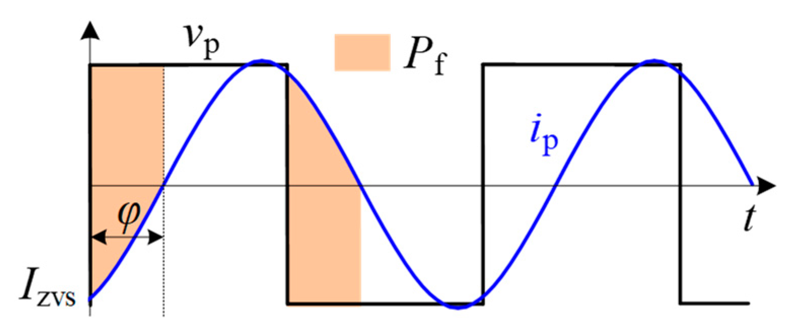
2.3. Operation Principle of ZVS Tracking

In order to realize ZVS, the primary coil current ip must be large enough to fully discharge the junction capacitors within the dead time before conducting the antiparallel diode. The required charge for a single MOSFET can be represented by the following expression:
Q r = 0 V in C o s s V ds d V ds
where Coss is the output capacitance and Vds is the drain-source voltage. It is difficult to directly calculate the output capacitance because Coss is a nonlinear function of Vds. However, according to the input voltage range listed in Table 1, it is justifiable to assume that the required charge Qr is constant with the MOSFETs datasheet given by manufactures.
Since the dead-time is short enough compared with the switching period, the switching current can be regarded as constant during the ZVS commutation time interval. Consequently, the average commutation current during the dead-time interval can be derived as:
I zvs 4 C oss V in ,   max t d
where td is the dead-time [37].
According to (11), Izvs is expected to be larger than the right side of (11) for the realization of ZVS. However, a larger Izvs means that more energy is fed back to the input supply by the resonant tank, posing a great challenge to the circuit components due to the high current and voltage stresses. Therefore, a minimized IZVS is the best choice for ZVS within the whole load range. In other words, when Izvs equals the right side of (11), despite the variation in the coupling coefficient and load resistance, the minimum requirement of ZVS would be satisfied. The minimum average commutation current during the dead-time interval should be the reference value used to design the control loop.

2.4. Limitation in Degree of Freedom for VF Control

To adapt to the wide range of output voltage and load resistance, the switching frequency must swing in a wide range for VF control. The typical operating waveforms of VF control are depicted in Figure 5.
Assuming ip(t) = Ipsin(ωtφ), the power that is fed back to the input voltage in one cycle period, T, can be expressed as
P f = V in T 0 φ ω i p t d t + π ω π + φ ω i p t d t
where Ip is the rms value of ip. Pf is represented by a light salmon color in the figure.
Similarly, the power transferred to the secondary side without considering the coil loss, can be written as
P t = V in T φ ω π ω i p t d t + π + φ ω 2 π ω i p t d t
At t = 0, Izvs can be obtained
I zvs = I p sin φ
By combining and solving (12)–(14), it is easy to obtain
P f = P t tan 2 φ 2
I zvs = P t V in tan φ 2
Figure 4a shows that when the switching frequency deviates from the natural resonant frequency (γ = 1), the input impedance angle φ increases dramatically. According to (15) and (16), when the power transferred from the primary side to secondary side Pt is constant, both Pf and Izvs increase with the increase in φ, resulting in higher reactive power losses.
As indicated before, there are two main objectives (CC-CV charging and ZVS) that should be achieved simultaneously to significantly improve the performance of the IPT system. Apparently, the degree of freedom for VF control cannot satisfy the above two objectives concurrently. Thus, an extra control variable should be introduced to increase the degree of freedom of control.

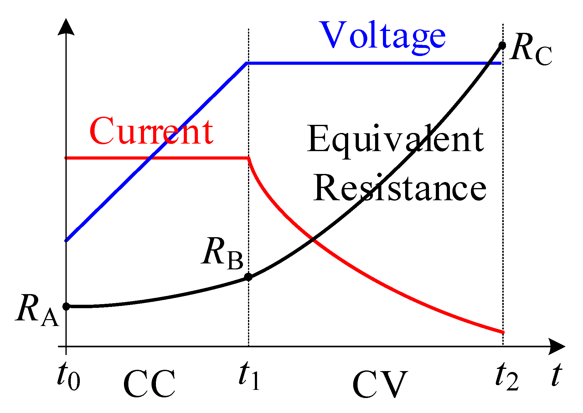
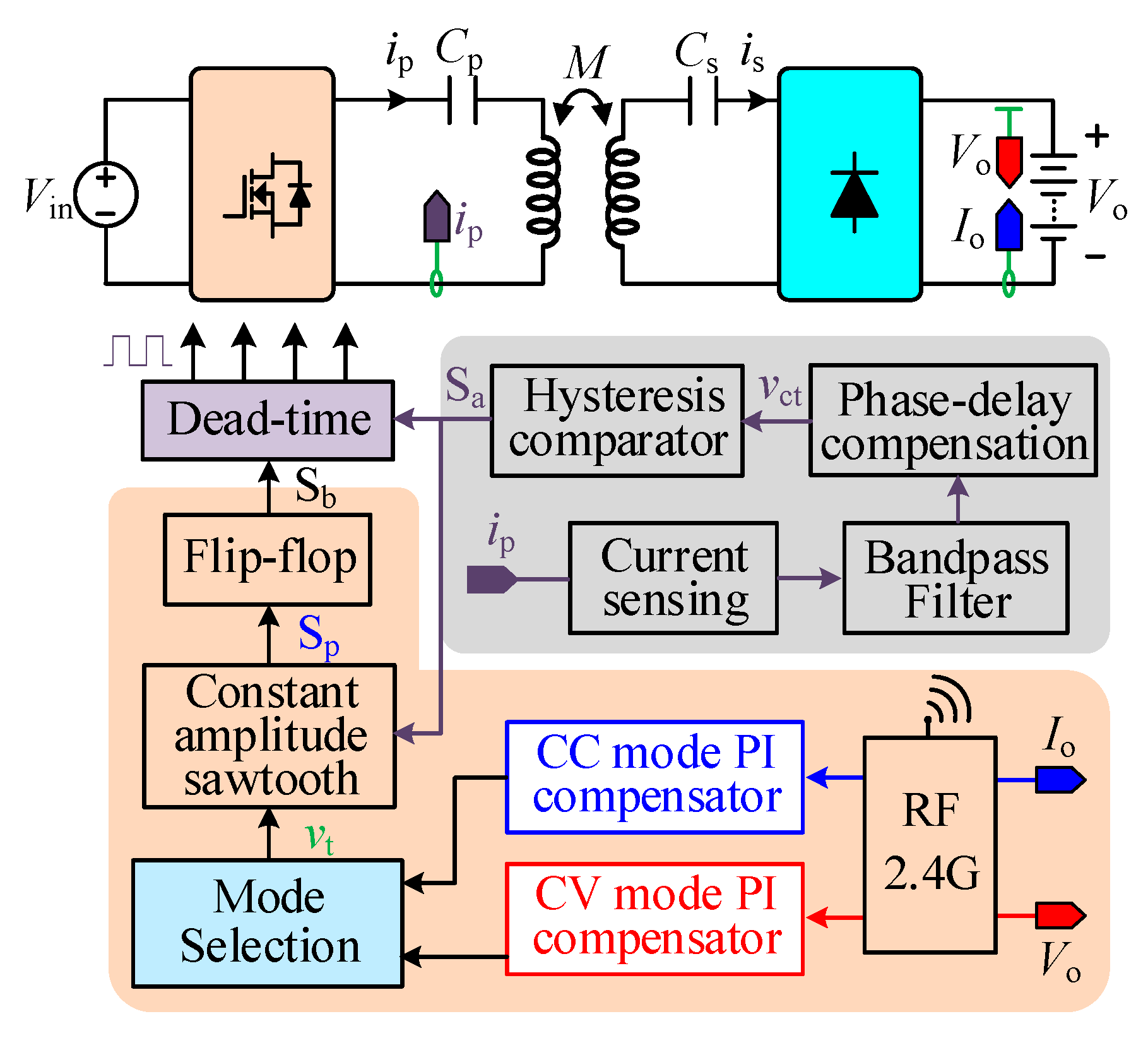
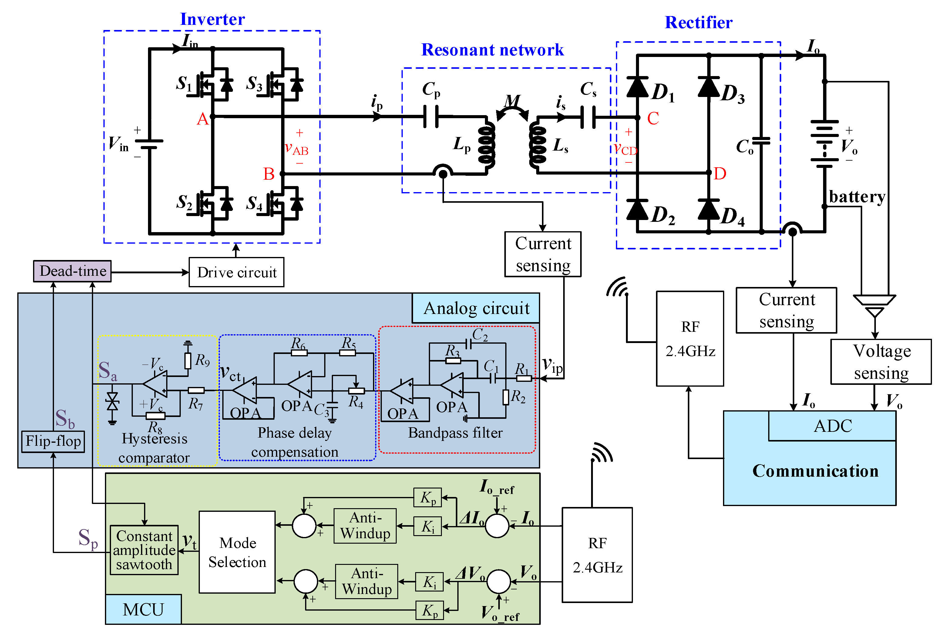
3. Implementation of Hybrid Control Strategy

To make the switching frequency close to the natural resonant frequency within the entire load range, in addition to the VF control, an extra PS control is used to regulate the output voltage/current. The key operation waveforms of the VF-PS control are plotted in Figure 6. G1–G4 represent the gate signals of power MOSFETs S1–S4, respectively, and vp,1 is the fundamental waveform of vp. The phase-shift angle θ is defined as the phase difference between the gate signals of switch pairs S2 and S4. It is worth noting that θ only affects the rms value of vp,1, which can be calculated as
v p , 1 = 2 2 π V in sin θ 2
Figure 6 illustrates that, at time t1, the gate signal G2 becomes zero. As the primary-side current ip is constant during the dead time interval, the junction capacitor on S1 starts to discharge, with a commutation current represented by iD1. The commutation current iD1 discharges the charge Qr during the dead time, preparing for the zero-voltage switch-on of S1. iD1 equals iD2, and iD3 equals iD4. In addition, it is obvious that iD3 is larger than iD1, which indicates that, if S1 can realize ZVS, all switches S1–S4 can realize ZVS.
From (6) and (17), the steady-state voltage gain G of VF-PS control can be rewritten as
G = j γ 3 k α sin θ 2 γ 4 k 2 α Q γ 2 1 2 α Q + j γ γ 2 1 α
According to (18), the 3D gain surfaces G against γ and θ under different loads are depicted in Figure 7. The red and blue curves are the contours of Gmax and Gmin. This shows that, with a constant γ, G will decrease as θ decreases. When θ is fixed, G shows a single-peak curve, as γ varies if the bifurcation phenomena do not exist [38]. Fortunately, G is a monotone decreasing function in the inductive region, i.e., γ > 1, which is crucial to ZVS operation. Theoretically, numerous combinations of γ and θ can fulfil the charging profile. However, only one possible combination can fulfil the charging profile. From Figure 7a to c, the load resistance ranges from 62.5 Ω to 800 Ω, which demonstrates that the analysis is valid throughout the whole charging process.

Self-Oscillating Phase Shift Control Strategy

On the basis of preceding analysis, there are two possible implementation schemes for VF-PS control strategy, which can be classified into the following types:
Type-I: The VF control loop is in charge of CC-CV charging while the PS control loop focuses on ZVS.
Type-II: The PS control loop is in charge of CC-CV charging while the VF control loop focuses on ZVS.
In this work, type-II is adopted.
Inspired by [36], the self-oscillating (SO) control strategy is employed to handle the ZVS operation. Unlike the traditional VF control, which externally imposes the switching frequency, SO control can always maintain ip lagging after the rising edge of vp. The stability of SO can be investigated using the extended Nyquist stability criterion [39,40] and is not discussed here. SO control also tunes the operating frequency. Therefore, SO-PS control is a kind of VF-PS control. Figure 8 illustrates the proposed SO-PS hybrid control diagram of the SS-compensated IPT charging system, where the grey region is analog circuit and light salmon region is MCU. It is known that the detection of a switching current ip(t1), used to obtain its instantaneous value at t1, is unnecessary, since it is easily disturbed by the circuit noise. In this implementation, the current ip is sampled by current sensing circuits and filtered through the bandpass filter. To compensate for the phase delay caused by the measurement circuits, a phase-delay compensation circuit is utilized, and its output signal is represented by vct. Triggered by vct, the hysteresis comparator will produce the driving signal Sa to drive the MOSFET S1 and S2, and the system frequency is determined by Sa.
Meanwhile, in the battery charging control loop, the smaller PI output between the CC mode and the CV mode is selected to determine which charging mode should remain. To be more specific, if the PI output of the CC loop is smaller than that of the CV loop, then CC mode will be selected. The PI value is determined by the integral of past difference between the reference value and the measured value. It is assumed that, initially, both the CC loop and CV loop have the minimum PI output and the reference values are higher than the initial values; this would mean that the differences are positive, which would result in an increment in the respective PI output. The system will start with the CC mode because the current will first reach its reference value and the difference between the reference current and measured current is zero; then, its PI output stops increasing. However, the voltage is far from its reference value at this stage, so the PI of the CV loop is saturated and remains at the maximum value, making it larger than that of the CC mode. Based on the principle that a smaller PI output will be selected, the mode selection picks up the CC mode accordingly. During the transition from a CC mode to a CV mode, as the system still operates at a CC mode and the equivalent load resistance keeps growing, the actual voltage exceeds the reference voltage, leading to a negative difference for the voltage control loop. Then, the PI output of the CV loop will become desaturated and begin to decrease until it becomes lower than that of the CC loop. From then on, the system switches to CV mode, and will not return to CC mode. Figure 9 illustrates the flow chart of the hybrid control strategy.
To show more details of the control circuit, Figure 10 illustrates the inner structure of important control units. It can be observed that the self-oscillation is completed by an analog circuit, and the phase shift is realized by a microprocessor. Each unit is analyzed as follows. The primary current is sampled by the current sensing circuit and the sinusoidal signal vip is first filtered by a bandpass filter to get rid of higher-order harmonics. Afterwards, to implement accurate control on the system, phase delay should be considered; therefore, a phase-delay compensation circuit is added, whose output is vct, as illustrated in Figure 11.
In contrast with the ZVS realization method reported in [28,29], the drive signal of the lagging leg is directly generated by a hysteresis comparator, and the corresponding hysteresis band width is determined by the minimal commutation current Izvs,ref, which can be calculated by
I zvs ,   ref = 4 C oss V inmax t d
The operation principle waveforms and hysteresis comparator circuit are shown in Figure 12. Vct is the output voltage signal of the phase-delay compensation circuit and input voltage signal of the hysteresis comparator, which satisfies vct = τip, where τ is a coefficient.
From Figure 12, the hysteresis band width Vb can be calculated by
V b = V ct R 7 R 8 = 4 τ C oss V inmax t d
In this specific design, Sa would be used to switch on S1 at the crossing point of Vb and vct. As vct represents ip, and Vb is proportional to Izvs,ref, the crossing point indicates that the primary-side current ip at this time equals Izvs,ref. If S1 can be switched on at this point, the commutation current at the rising edge of vp equals Izvs,ref, and can be used to realize ZVS. The same is true for S2: at the falling edge of Sa, the primary-side current ip equals Izvs,ref again, and can guarantee the ZVS of S2.
In order to achieve CC-CV charging, the falling edge of vp should be determined as well. In other words, the gate signal of S3(S4) and Sa must be synchronized with a controllable phase delay θ. The practical implementation waveforms are given in Figure 13. The main idea of the synchronization method is to generate a constant-amplitude sawtooth Sw according to the variations in switching frequency in a microprocessor. Hence, the PI output of the CC/CV charging loop vt can be compared with Sw, resulting in a pulse Sp. The pulse Sp is used to set and reset a flip-flop whose output is defined as Sb. Sb would be used to control the turning on and off for S3 and S4. Consequently, both Sa and Sb input the dead-time module to define the gate signals, which can avoid any probability of the shoot-through of the MOSFETs.
Based on the implementation given above, the IPT system with a hybrid control strategy can achieve ZVS and CC/CV output simultaneously.

4. Experimental Verifications

As shown in Figure 14, a 1.6-kW IPT battery charging system was designed and built to validate the proposed hybrid control strategy. Two rectangular coils, separated by a 10–15 cm air gap, were used to couple the primary side with the secondary side. Both coupled coils are formed of a 600-strand Litz wire, and the coils are 30 cm × 25 cm in size. The thickness of the coils is about 10 mm, including the ferrite bars. The primary coil has 18 turns, and the secondary coil has 24 turns.
The electrical parameters of the prototype system are listed in Table 2. The primary coil current ip is measured using the current transducer LA-25P with galvanic separation. A sampling circuit is employed on the primary side. A DC source (Chroma 62150H) is employed, and an electric load (Chroma 63206E) serves as the adjustable load resistor.
Before the battery charger operation, the amplitude of the primary coil current is zero, and no signal can be employed to start the oscillations. Hence, a starting process should be applied to provide initial driving signals. Here, S2 and S3 switches are turned on: vp = −Vin. Then, S1 and S4 are turned on, while S2 and S3 are turned off. The inverter applies a step voltage to the resonant network with an amplitude of the input voltage. The state of the switches is changed when the rising edge of Sa is detected, meaning that the inverter is undergoing a self-oscillation operation.

4.1. Operation Waveforms

According to (25) and the datasheet of the adopted MOSFETs, the minimal commutation current Izvs,ref can be determined as 3 A when considering some margins. The steady-state operation waveforms of the IPT charging system at different k conditions are shown in Figure 15. The charging current is 4 A in CC mode and the charging voltage is 400 V in CV mode, regardless of k. The critical coupling coefficient can be calculated as kc = 0.25. As seen from Figure 15a,c, when k = 0.2, this means that bifurcation did not occur and the communication current Izvs is approximately 3.10 A and 3.11 A. In Figure 15b,d, k = 0.3 > kc, which means that bifurcation occurred, and the measured switching frequency is 94.6 kHz, i.e., γ = 1.24. In addition, the communication current Izvs is about 2.95 A and 2.87 A.
To verify the robust performance of the proposed hybrid control method, experimental results were measured with a Vin that changed from 380 V to 420 V when k = 0.3. As shown in Figure 16a, Io can be maintained at a steady state of 4 A with a slight overshoot when the input voltage changes in CC mode. The communication currents Izvs are 2.9 A and 3.1 A. Similarly, the output voltage Vo is almost unchanged in CV mode, as shown in Figure 16b. The communication currents Izvs are 2.85 A and 3.07 A, respectively. The response time of the control system is around 40 ms.
The experimental results were measured when the load suddenly changed, as shown in Figure 17. It should be emphasized that the equivalent resistance of the battery pack cannot abruptly change in practical applications. Here, the sudden change in the equivalent resistance RL was only used to test the dynamic performance of the proposed control strategy. Figure 17 shows that the proposed IPT system can maintain a constant output current in CC mode and a constant output voltage in CV mode when the load changes. From the enlarged view of Figure 17a,b, it is clear that ZVS is achieved. The response time of RL changed in CC mode in the control system is around 320 ms, and the response time of RL changed in CV mode in the control system is around 20 ms.
The CC mode will be switched to CV mode when the battery voltage is increased to 400 V. Figure 18 shows that the CC mode can be smoothly changed to CV mode by comparing the corresponding PI values. Clearly, the ZVS is obtained with Izvs = 3.01 A and Izvs = 2.88 A. The response time of CC mode changing to CV mode in the control system is around 160 ms.
To testify the control accuracy of ZVS, the communication current errors ΔIzvsIzvs = IzvsIzvsref) were measured under various conditions, maintaining CC/CV battery charging, as shown in Figure 19. The maximum current error is about 0.2 A in comparison with the preset value.
The measured normalized switching angle frequency γ of the proposed hybrid control and VF control for different coupling coefficient k and input voltage Vin are plotted in Figure 20. For VF control, γ decreases gradually in CC mode while it remains approximately constant in CV mode, in accordance with the theoretical analysis in Section 2. For the proposed hybrid control, γ decreases over the whole charging process and moves towards γ = 1. It is easy to see that the switching frequency of the proposed hybrid control is much closer to the natural resonant frequency than that of VF control, which reduces the reactive power loss. The triangles and diamonds are sampling points.

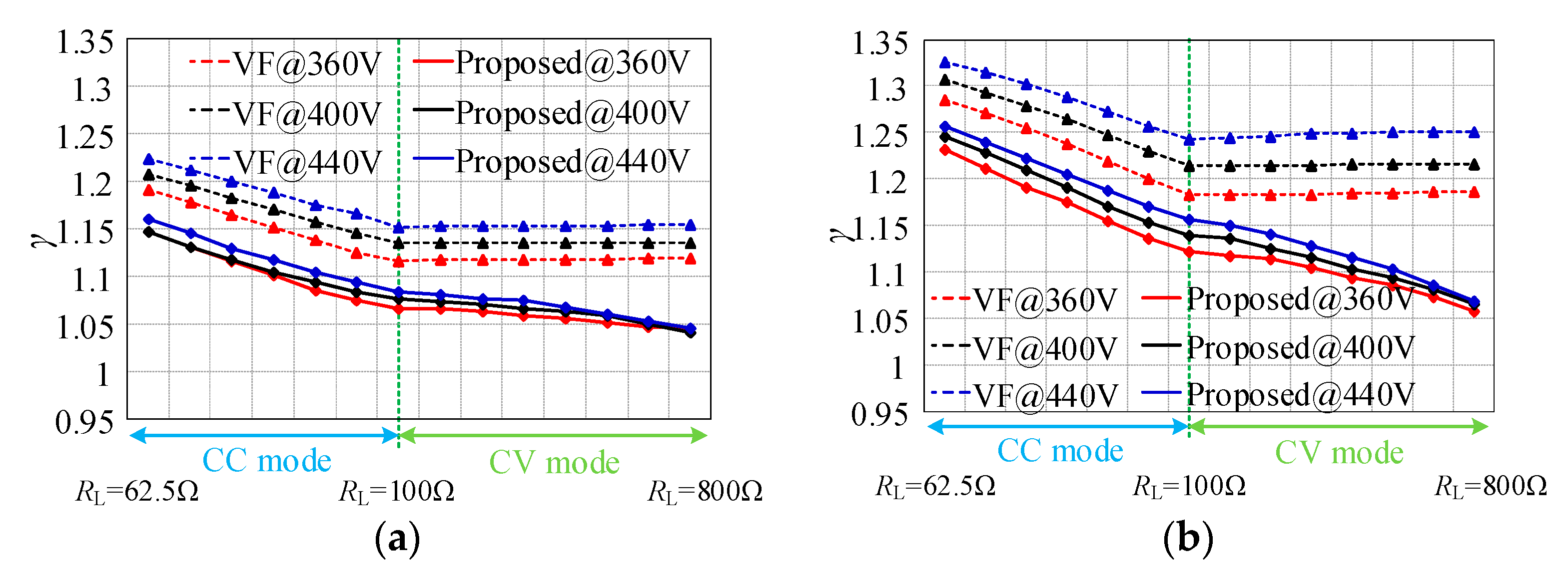
4.2. System Efficiency

The measured system efficiency of the proposed hybrid control and the conventional VF control are shown in Figure 21. The experimental results show that the maximum efficiency of the proposed control is 96.7% when Vin = 360 V, k = 0.3, and Po = 1. reaches 6 kW in CC mode. Compared with conventional VF control, the maximum efficiency improvement in the proposed hybrid control is approximately 2.9% in CC mode, while it is 4.1% in CV mode. The results show that the adoption of phase shift control can provide a more flexible way to achieve the constant output control target. The triangles and diamonds are sampling points.

5. Discussion

The hybrid control strategy has been widely used in the SS-compensated IPT charging system since, compared with a single-variable control strategy such as VF control, an additional control variable can provide more degrees of freedom, which contributes to achieving the control target. For example, in this work, with the help of phase shift control, the operating frequency is closer to the natural resonant frequency, reducing the reactive power. Some of the existing literature applied their hybrid control model to the full-bridge inverter to tune the operating frequency, whereas some used additional components, such as a variable inductor or capacitor, to change the parameters of the compensation network with a constant operating frequency. The control strategies mentioned above adjust the phase angle between the primary inverter voltage and current. The advantage of the frequency-tuning method is the elimination of power loss produced by additional components, and the advantage of the variable inductor or capacitor methods is to the avoid potential instability caused by bifurcation issues. Table 3 provides a comparison to other control strategies.
For the future scope and an insight into the further developments, in this work, a hybrid control strategy is studied and implemented. However, there is not adequate research on the modelling of the control system and parameter design. In order to optimize the system parameter, reduce the response time, and increase the system efficiency, it is necessary to build up the system modelling to improve the system performance and corresponding experiments should be conducted to demonstrate the effectiveness of the modelling.

6. Conclusions

An SO-PS hybrid control strategy for an SS-compensated IPT system is studied and implemented in this paper to realize CC-CV battery charging and ZVS simultaneously. The hybrid control makes the switching frequency close to the resonant frequency throughout the whole charging process. The commutation current for ZVS always remains constant, regardless of the variation in the coupling coefficient and the load. Hardware implementation was carried out, and the effectiveness of the proposed control strategy was verified by an experimental prototype. The maximum efficiency is 96.7%, with Vin = 360 V, k = 0.3, and Po = 1.6 kW.

Author Contributions

Conceptualization, L.H.; supervision, C.-K.L.; visualization, X.W. All authors have read and agreed to the published version of the manuscript.

Funding

This research was funded by Theme-based Research Scheme (T23-701/20-R).

Institutional Review Board Statement

Not applicable.

Informed Consent Statement

Not applicable.

Data Availability Statement

No new data were created or analyzed in this study. Data sharing is not applicable to this article.

Conflicts of Interest

The authors declare no conflict of interest.

Abbreviations

The following abbreviations are used in this manuscript:
IPTInductive power transfer
ZVSZero voltage switching
CCConstant current
CVConstant voltage
SOSelf-oscillating
PSPhase shift
SSSeries-series
VFVariable frequency
EVElectric vehicle
EMIElectromagnetic interference
ZPAZero phase angle
PWMPulse width modulation
PDMPulse density modulation
PLLPhase-locked loop
VIVariable inductor
FHAFundamental harmonic approximation
VinDC input voltage
Siith MOSFET in the inverter
CpPrimary-side capacitor
LpTransmitter coil
LsReceiver coil
CsSecondary-side capacitor
Diith diode in the rectifier
CoOutput filter capacitor
VoCharging voltage
IoCharging current
vpInverter output voltage
ipInverter output current
vsRectifier input voltage
isRectifier input current
RacEquivalent load resistance
MMutual Inductance
ωSwitching angular frequency of the system
IzvsCommutation current
αInductance ratio of transmitter coil over receiver coil
γNormalized switching frequency
XLsImpedance of receiver coil
QLoad quality factor
GvSteady-state voltage gain
φInput impedance angle
kCoupling coefficient
dAir gap
DoutMaximum coil diameter
RLLoad resistance
QrCharge on the parasitic capacitor of the MOSFET
CossCapacitance of parasitic capacitor of the MOSFET
VdsDrain-source voltage of the parasitic capacitor of the MOSFET

References

  1. Ahn, D.; Hong, S. Wireless power transmission with self-regulated output voltage for biomedical implant. IEEE Trans. Ind. Electron. 2014, 61, 2225–2235. [Google Scholar] [CrossRef]
  2. Xiao, C.; Cheng, D.; Wei, K. An LCC-C compensated wireless charging system for implantable cardiac pacemakers: Theory, experiment, and safety evaluation. IEEE Trans. Power Electron. 2018, 33, 4894–4905. [Google Scholar] [CrossRef]
  3. Jang, Y.; Jovanovic, M.M. A contactless electrical energy transmission system for portable-telephone battery chargers. IEEE Trans. Ind. Electron. 2003, 50, 520–527. [Google Scholar] [CrossRef] [Green Version]
  4. Hui, S.Y.R.; Ho, W.W.C. A new generation of universal contactless battery charging platform for portable consumer electronic equipment. IEEE Trans. Power Electron. 2005, 20, 620–627. [Google Scholar] [CrossRef]
  5. Zhao, L.; Thrimawithana, D.; Madawala, U. Hybrid bidirectional wireless EV charging system tolerant to pad misalignment. IEEE Trans. Ind. Electron. 2017, 64, 7079–7086. [Google Scholar] [CrossRef]
  6. Guo, Y.; Wang, L.; Zhu, Q.; Liao, C.; Li, F. Switch-on modeling and analysis of dynamic wireless charging system used for electric vehicles. IEEE Trans. Ind. Electron. 2016, 63, 6568–6579. [Google Scholar] [CrossRef]
  7. Chen, C.; Zhou, H.; Deng, Q.; Hu, W.; Yu, Y.; Lu, X.; Lai, J. Modeling and decoupled control of inductive power transfer to implement constant current/voltage charging and zvs operating for electric vehicles. IEEE Access 2018, 6, 59917–59928. [Google Scholar] [CrossRef]
  8. Li, Z.; Zhu, C.; Jiang, J.; Song, K.; Wei, G. A 3-kW wireless power transfer system for sightseeing car supercapacitor charge. IEEE Trans. Power Electron. 2017, 32, 3301–3316. [Google Scholar] [CrossRef]
  9. Kim, J.H.; Lee, B.S.; Lee, J.H.; Lee, S.H.; Park, C.B.; Jung, S.M.; Lee, S.G.; Yi, K.P.; Baek, J. Development of 1-MW inductive power transfer system for a high-speed train. IEEE Trans. Ind. Electron. 2015, 62, 6242–6250. [Google Scholar] [CrossRef]
  10. Jiang, Y.; Chen, K.; Zhao, Z.; Yuan, L.; Tan, T.; Lin, Q. Designing an M-Shape Magnetic Coupler for the Wireless Charging System in Railway Applications. IEEE Trans. Power Electron. 2022, 37, 1059–1073. [Google Scholar] [CrossRef]
  11. Chan, C.C.; Jian, L.; Tu, D. Smart charging of electric vehicles—Integration of energy and information. IET Electr. Syst. Transp. 2014, 4, 89–96. [Google Scholar] [CrossRef] [Green Version]
  12. He, L.; Zhao, S.; Wang, X.; Lee, C.-K. Artificial Neural Network-Based Parameter Identification Method for Wireless Power Transfer Systems. Electronics 2022, 11, 1415. [Google Scholar] [CrossRef]
  13. Bosshard, R.; Kolar, J.W. Inductive power transfer for electric vehicle charging: Technical challenges and tradeoffs. IEEE Power Electron. Mag. 2016, 3, 22–30. [Google Scholar] [CrossRef]
  14. Al-Saadi, M.; Al-Omari, A.; Al-Chlaihawi, S.; Al-Gizi, A.; Crăciunescu, A. Inductive Power Transfer for Charging the Electric Vehicle Batteries. Electroteh. Electron. Autom. 2018, 66, 29–39. [Google Scholar]
  15. Jiang, Y.; Wang, L.; Wang, Y.; Liu, J.; Li, X.; Ning, G. Analysis, design, and implementation of accurate ZVS angle control for EV battery charging in wireless high-power transfer. IEEE Trans. Ind. Electron. 2019, 66, 4075–4085. [Google Scholar] [CrossRef]
  16. Wang, X.; He, L.; Xu, J.; Lee, C.K. Widening the Operating Range of a Wireless Charging System Using Tapped Transmitter Winding and Bifrequency Pulse Train Control. IEEE Trans. Power Electron. 2022, 37, 13874–13883. [Google Scholar] [CrossRef]
  17. Deng, P.; Tang, C.; Fan, Y.; Sun, M.; Liu, Z.; Li, X. A Frequency Regulation Strategy for Dynamic Process Noise Suppression in LCC-S WPT Systems. IEEE Trans. Power Electron. 2022, 37, 13978–13988. [Google Scholar] [CrossRef]
  18. Qu, X.; Han, H.; Wong, S.; Tse, C.K.; Chen, W. Hybrid IPT topologies with constant current or constant voltage output for battery charging applications. IEEE Trans. Power Electron. 2015, 30, 6329–6337. [Google Scholar] [CrossRef]
  19. Mai, R.; Chen, Y.; Li, Y.; Zhang, Y.; Cao, G.; He, Z. Inductive Power Transfer for Massive Electric Bicycles Charging Based on Hybrid Topology Switching with a Single Inverter. IEEE Trans. Power Electron. 2017, 32, 5897–5906. [Google Scholar] [CrossRef]
  20. Chen, Y.; Yang, B.; Li, Q.; Feng, H.; Zhou, X.; He, Z.; Mai, R. Reconfigurable Topology for IPT System Maintaining Stable Transmission Power over Large Coupling Variation. IEEE Trans. Power Electron. 2020, 35, 4915–4924. [Google Scholar] [CrossRef]
  21. Qu, X.; Jing, Y.; Han, H.; Wong, S.; Tse, C.K. Higher order compensation for inductive-power-transfer converters with constant-voltage or constant-current output combating transformer parameter constraints. IEEE Trans. Power Electron. 2017, 32, 394–405. [Google Scholar] [CrossRef]
  22. Vu, V.; Tran, D.; Choi, W. Implementation of the constant current and constant voltage charge of inductive power transfer systems with the double-sided LCC compensation topology for electric vehicle battery charge applications. IEEE Trans. Power Electron. 2018, 33, 7398–7410. [Google Scholar] [CrossRef] [Green Version]
  23. Song, K.; Li, Z.; Jiang, J.; Zhu, C. Constant current/voltage charging operation for series–series and series–parallel compensated wireless power transfer systems employing primary-side controller. IEEE Trans. Power Electron. 2018, 33, 8065–8080. [Google Scholar] [CrossRef]
  24. Gati, E.; Kampitsis, G.; Manias, S. Variable Frequency Controller for Inductive Power Transfer in Dynamic Conditions. IEEE Trans. Power Electron. 2017, 32, 1684–1696. [Google Scholar] [CrossRef]
  25. Li, H.; Wang, K.; Fang, J.; Tang, Y. Pulse density modulated ZVS full-bridge converters for wireless power transfer systems. IEEE Trans. Power Electron. 2019, 34, 369–377. [Google Scholar] [CrossRef]
  26. Xu, L.; Chen, Q.; Ren, X.; Wong, S.; Tse, C.K. Self-oscillating resonant converter with contactless power transfer and integrated current sensing transformer. IEEE Trans. Power Electron. 2017, 32, 4839–4851. [Google Scholar] [CrossRef]
  27. Namadmalan, A. Self-oscillating tuning loops for series resonant inductive power transfer systems. IEEE Trans. Power Electron. 2016, 31, 7320–7327. [Google Scholar] [CrossRef]
  28. Chen, Q.; Wong, S.C.; Tse, C.K.; Ruan, X. Analysis, design, and control of a transcutaneous power regulator for artificial hearts. IEEE Trans. Biomed. Circuits Syst. 2009, 3, 23–31. [Google Scholar] [CrossRef]
  29. Namadmalan, A. Self-Oscillating Pulsewidth Modulation for Inductive Power Transfer Systems. IEEE Trans. Emerg. Sel. Topics Power Electron. 2020, 8, 1813–1820. [Google Scholar] [CrossRef]
  30. Jiang, Y.; Wang, L.; Wang, Y.; Liu, J.; Wu, M.; Ning, G. Analysis, design, and implementation of WPT system for EV’s battery charging based on optimal operation frequency range. IEEE Trans. Power Electron. 2019, 34, 6890–6905. [Google Scholar] [CrossRef]
  31. Jiang, Y.; Liu, J.; Hu, X.; Wang, L.; Wang, Y.; Ning, G. An optimized frequency and phase shift control strategy for constant current charging and zero voltage switching operation in series-series compensated wireless power transmission. IEEE Energy Convers. Congr. Expo. 2017, 961–966. [Google Scholar]
  32. Li, Y.; Sun, W.; Zhu, X.; Hu, J. A Hybrid Modulation Control for Wireless Power Transfer Systems to Improve Efficiency Under Light-Load Conditions. IEEE Trans. Ind. Electron. 2022, 69, 6870–6880. [Google Scholar] [CrossRef]
  33. Li, Y.; Liu, S.; Zhu, X.; Hu, J.; Zhang, M.; Mai, R.; He, Z. Extension of ZVS Region of Series–Series WPT Systems by an Auxiliary Variable Inductor for Improving Efficiency. IEEE Trans. Power Electron. 2021, 36, 7513–7525. [Google Scholar] [CrossRef]
  34. Kavimandan, U.D.; Mahajan, S.M.; Van Neste, C.W. Analysis and Demonstration of a Dynamic ZVS Angle Control Using a Tuning Capacitor in a Wireless Power Transfer System. IEEE Trans. Emerg. Sel. Topics Power Electron. 2021, 9, 1876–1890. [Google Scholar] [CrossRef]
  35. Ganapathee, M.; Alavandar, S.; Kasinathan, P.; Sowmmiya, U.; Ramachandaramurthy, V.K.; Pachaivannan, N. Evaluation of hybrid controllers for space vector modulation-inverter driven permanent magnet synchronous motor-pump assembly. ISA Trans. 2022, 128, 635–649. [Google Scholar] [CrossRef]
  36. Zhang, W.; Wong, S.C.; Tse, C.K. Chen. Design for Efficiency Optimization and Voltage Controllability of Series–Series Compensated Inductive Power Transfer Systems. IEEE Trans. Power Electron. 2014, 29, 191–200. [Google Scholar] [CrossRef]
  37. Li, S.; Li, W.; Deng, J.; Nguyen, T.D.; Mi, C.C. A Double-Sided LCC Compensation Network and Its Tuning Method for Wireless Power Transfer. IEEE Trans. Veh. Technol. 2015, 64, 2261–2273. [Google Scholar] [CrossRef]
  38. Wang, C.-S.; Covic, G.A.; Stielau, O.H. Power transfer capability and bifurcation phenomena of loosely coupled inductive power transfer systems. IEEE Trans. Ind. Electron. 2004, 51, 148–157. [Google Scholar] [CrossRef]
  39. Youssef, M.Z.; Pinheiro, H.; Jain, P.K. Self-sustained phase-shift modulated resonant converters: Modeling, design, and performance. IEEE Trans. Power Electron. 2006, 21, 401–414. [Google Scholar] [CrossRef]
  40. Youssef, M.Z.; Jain, P.K. Series–parallel resonant converter in self-sustained oscillation mode with the high-frequency transformer- leakage-inductance effect: Analysis, modeling, and design. IEEE Trans. Ind. Electron. 2007, 54, 1329–1341. [Google Scholar] [CrossRef]
Figure 1. Circuit architecture of SS-compensated IPT charging system.
Sustainability 15 03606 g001
Figure 2. The ac equivalent circuit of the SS-compensated IPT system.
Sustainability 15 03606 g002
Figure 3. The simplified battery charging profile.
Sustainability 15 03606 g003
Figure 4. The curve of (a) φ (b) Gv versus different load resistance RL.
Sustainability 15 03606 g004
Figure 5. The typical operation waveforms of VF control.
Sustainability 15 03606 g005
Figure 6. The typical operating waveforms of VF-PS control.
Sustainability 15 03606 g006
Figure 7. The 3-D gain surfaces G against γ and θ under different loads. (a) Vo = 250 V, Io = 4 A. (b) Vo = 400 V, Io = 4 A. (c) Vo = 400 V, Io = 0.5 A.
Sustainability 15 03606 g007
Figure 8. The diagram of IPT charging system with SO-PS control.
Sustainability 15 03606 g008
Figure 9. Flow chart of SO-PS control strategy.
Sustainability 15 03606 g009
Figure 10. Proposed control circuit for IPT system.
Sustainability 15 03606 g010
Figure 11. Schematic diagrams of Bandpass filter and phase-delay compensation circuit.
Sustainability 15 03606 g011
Figure 12. Schematic diagrams of hysteresis comparator circuit and waveform.
Sustainability 15 03606 g012
Figure 13. Practical implementation waveforms of synchronization.
Sustainability 15 03606 g013
Figure 14. Experimental prototype of the proposed IPT charging system.
Sustainability 15 03606 g014
Figure 15. Experimental waveforms at Vin = 400 V condition. (a) CC mode, k = 0.2, (b) CC mode, k = 0.3, (c) CV mode, k = 0.2, and (d) CV mode, k = 0.3.
Sustainability 15 03606 g015
Figure 16. Experimental waveforms at k = 0.3 conditions when Vin changes from 380 V to 420 V. (a) CC mode, (b) CV mode.
Sustainability 15 03606 g016
Figure 17. Experimental waveforms at k = 0.3, Vin = 400 V condition. (a) In CC mode when the RL changes from 75 Ω to 95 Ω, (b) in CV mode when the RL changes from 105 Ω to 265 Ω.
Sustainability 15 03606 g017
Figure 18. Experimental waveforms from CC mode to CV mode.
Sustainability 15 03606 g018
Figure 19. Steady-state communication currents errors of Izvs.
Sustainability 15 03606 g019
Figure 20. The measured switching frequency of proposed hybrid control and VF control. (a) k = 0.2, (b) k = 0.3.
Sustainability 15 03606 g020
Figure 21. The measured overall efficiency of the IPT charging system. (a) k = 0.2, (b) k = 0.3.
Sustainability 15 03606 g021
Table 1. Electrical specifications.
ParametersSymbolValue
Input voltage VinVin_min − Vin_max360–440 V
Output voltage VoutVout_min − Vout_max250–400 V
Maximum output powerPo_max1.6 kW
Air gapd10–15 cm
Maximum coil diameterDout30 cm
Load resistanceRL62.5–800 Ω
Table 2. Electrical parameters of the prototype.
ParametersSymbolValue
Primary coil inductorLp239.7 μH
Primary compensation capacitorCp18.7 nF
Secondary coil inductorLs332.1 μH
Secondary compensation capacitorCs13.5 nF
Coupling coefficientk0.2–0.3
Power MOSFETsS1–S4FCH76N60NF
Rectifier diodesD1–D4DSEI120-06A
Table 3. Comparison with other relevant control techniques.
Control
Strategy
Input
Voltage
Maximum
Power
Battery
Voltage
System
Efficiency
Output
Type
[28] PWM-PLL30–60 V60 W24 V87.8%CV
[29]SOS PS-PWM50 V220 W50 V88%CV
[31]VF-PS80 V288 W32–72 V94.9%CC-CV
[33]VI-PS100 V170 W72 V92%CV
[34]SC-PS30 V10 W26 V87%CC-CV
This workSO-PS360–440 V1.6 kW250–400 V96.7%CC-CV
Disclaimer/Publisher’s Note: The statements, opinions and data contained in all publications are solely those of the individual author(s) and contributor(s) and not of MDPI and/or the editor(s). MDPI and/or the editor(s) disclaim responsibility for any injury to people or property resulting from any ideas, methods, instructions or products referred to in the content.

