1. Introduction
Climate change and air pollution are of significant concern to our modern society. The increasing environmental awareness along with the penetration of electric vehicles in terms of market share has the potential to bring about a significant reduction of CO
2 emissions. The CO
2 footprint of the transportation sector alone contributes almost 25% of the total CO
2 resulting from fossil fuels [
1]. Vehicles equipped with the internal combustion engine (ICE) have been in existence for a long time. Their progressive substitution by electric vehicles can reduce CO
2 emissions drastically, improving air quality and reducing air pollution. Furthermore, the efficiency and performance of the electric motor are higher than those of the ICE. Energy utilization of electric vehicles reaches up to 80–85% compared to 12.3% for the ICE [
2].
A current obstacle that hinders the widespread adoption of electric vehicle ownership is the lack of proper EV charging infrastructure that can replace and compete with existing petrol stations, especially on highways where long-distance driving is required. Electric vehicle battery charging is categorized into three categories based on maximum charging power: slow, medium, and fast chargers. Slow and medium chargers are typically mounted on board owing to lower ratings; components are traditionally smaller and lighter in weight. On the other hand, fast chargers can only be off-board due to high-power components and special infrastructure that cannot be included in car space. On-board battery chargers typically consist of two consecutive stages, an AC-DC stage followed by an isolated DC-DC converter for regulating the charging current. Ref. [
3] describes a
two-stage plug-in hybrid electric vehicle (PHEV) charger based on an interleaved AC-DC boost PF corrector followed by an isolated DC-DC converter. The DC-DC converter at the second stage is implemented using a full-bridge topology based on [
4]. A drawback of such a topology is the bulky capacitor. In order to overcome this problem, a full-bridge LLC resonant converter with boost PF corrector is developed in [
5] and a high-frequency resonant converter with a boost converter for regulating the charging of EV is discussed in [
6]. On-board chargers can directly be connected to single- or three-phase mains, which eases usage and reduces infrastructure cost. However, the on-board charger has a long charging time that reaches up to several hours; additionally, the mounted charger weight impacts the car weight and thus performance.
On the other hand, off-board chargers are installed in dedicated charging stations, which are designed to offer higher charging power capabilities, yet at higher installation and operational cost. DC fast charging has been extensively discussed in the literature due to its advantages over existing conventional gas stations. There exist many off-board charger topologies. Typically, off-board chargers constitute two consecutive stages for isolation; the first is an AC-DC stage, followed by a DC-DC conversion stage to regulate and control the charging. The charging station can either share a common AC link (after the first stage) or a common DC link (after the second stage) [
7]. DC link charging stations are more common, since DC-connected chargers are of higher efficiency due to the reduced number of power conversion stages, absence of reactive power, which simplifies control, and reduced installation cost [
8]. Another prominent advantage of DC distribution systems is the opportunity to use partial power converters to process only a portion of the power processed to the vehicle, reducing the converter ratings and thus the cost. Partial power processing has addressed the common cost issue of fast charging stations as well as improving the overall station efficiency. Furthermore, these converters have less impact on the grid since the current withdrawn from the grid has less distortion as will be proved in this paper. Converters designed at partial power have been proposed in [
9] based on a cascaded H-bridge interfaced to an AC medium voltage grid with dual active bridge (
DAB) to control the DC link followed by a full bridge to control the charging operation. In this topology, the charging power flows through the
DAB followed by the full bridge, while the medium voltage cascaded bridge is designed at the rated power of the charging station. In [
10], a multi-port AC-DC converter with DC-DC differential power converters were investigated for PV systems integrated with batteries and connected to the grid. In this topology, the DC-DC converter is used to control the active power flow through the battery. The DC-DC converter is connected to a DC-AC port to interface between the battery and the AC grid. This topology, however, has cascaded conversion, which, in return, impacts efficiency. Furthermore, a ring-connected dual active bridges-based multiport converter is reported in [
11], where it offers high redundancy and availability due to existence of two power paths for each port. Another ring topology has been proposed in [
12] with PV system integration at each port. This topology illustrates how the integration of DC charging station with PV panels can be implemented, yet the power transfer capability from the PV side is limited. An AC source must be considered as the fast charging system unless a large storage is built which results in reduced overall system efficiency due to multi conversion stages. Additionally, due to multi-winding transformer usage, unbalanced winding requires a special winding design to minimize current circulation between windings. Moreover, another topology composed of a three-level neutral point clamped converter has been presented in [
13]. All the previous power DC-DC converters in the literature for off-board chargers have cascaded power processing stages resulting in reduced efficiency and increased system complexity. Nevertheless, partial power-rated DC-DC converters are used to control the charge over each EV battery by processing only a fraction of the total battery demand as discussed in the literature; partial power processing has been integrated in PV applications as discussed in [
14,
15], in data center power distribution schemes [
16,
17,
18], and in electric vehicle off-board chargers as discussed in [
19]. In [
19], the partial power converter used is a unidirectional LLC converter which shares the same DC link capacitor. This topology is unidirectional and it requires passive components of L and C to be with very low tolerance. Furthermore, differential power processing architecture is illustrated in [
20] with multiport half bridge unidirectional DC-DC conversion stages that share a common DC link. This topology suffers high stress on the power switches used in the half-bridge auxiliary converters.
Another approach is proposed in [
21], with a combination of dual active bridges (
DAB) with triple active bridge (TAB) DC-DC converters. This topology has cascaded conversion stages with a multi-winding transformer intermediate AC stage. Due to this converter cascading, losses inside the system increase along with the system investment cost.
In this paper, a novel power delivery scheme has been proposed based on differential power processing DC-DC converters to control the charging/discharging of the batteries connected. The proposed system consists of two converters (main and auxiliary converter). The auxiliary converter selected is dual active bridge (DAB) sized at partial power rating of the charger. The main converter is a bidirectional buck converter designed at full power of the charger and will change its output voltage depending on the occupied ports to meet different kinds of series states, while maintaining the main DC source in the system constant. The buck converter output voltage is automatically adjusted. The topology is expandable and can accommodate as many charging slots as desired. This approach eliminates the cascaded converter approach in the aforementioned systems; it can also considerably off-load the infrastructure and operation costs and simultaneously improves the overall system efficiency. The specific contributions of this paper can be listed as follows:
A novel bi-directional, series-type scheme that regulates the charging process by controlling only a fraction of the charging power, while the remaining power is delivered to the battery via an external loop.
The proposed topology offers high efficiency, lower cost, and the capability of providing fault tolerance.
A scaled-down prototype is designed, and experimental results are discussed from the prototype to validate the better performance of the proposed system
2. Proposed System Overview
In this section, the concept of partial power processing has been investigated in order to process the load power with the minimum converter rating possible.
- 1.
Charger architectures
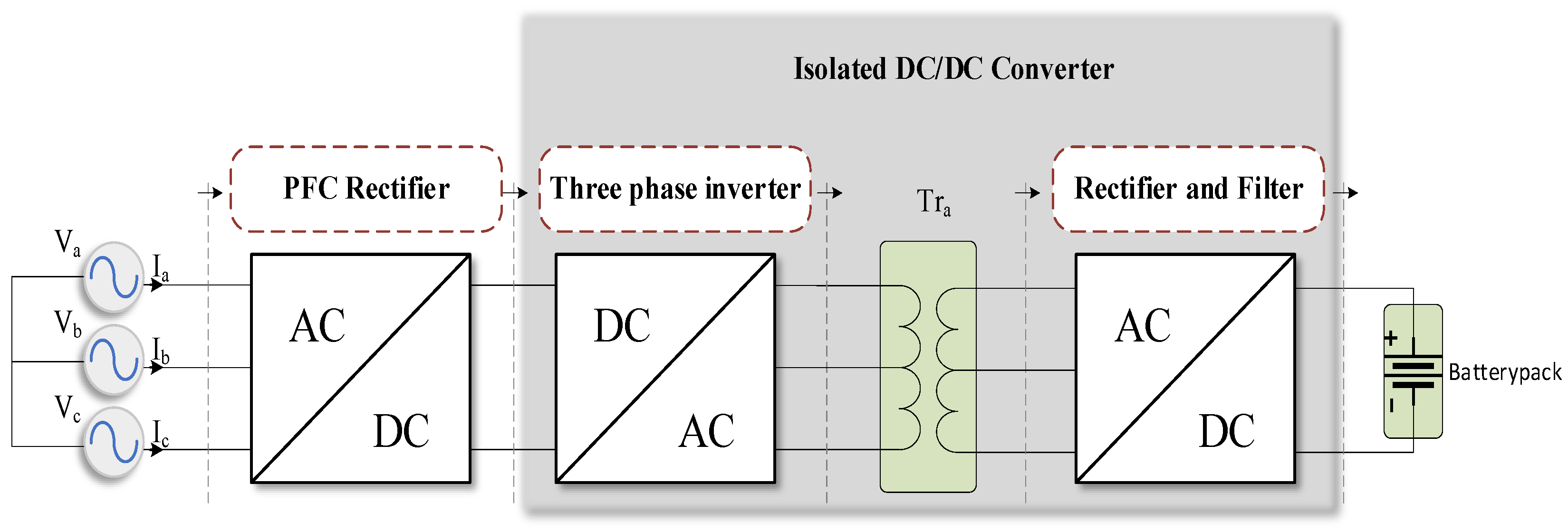
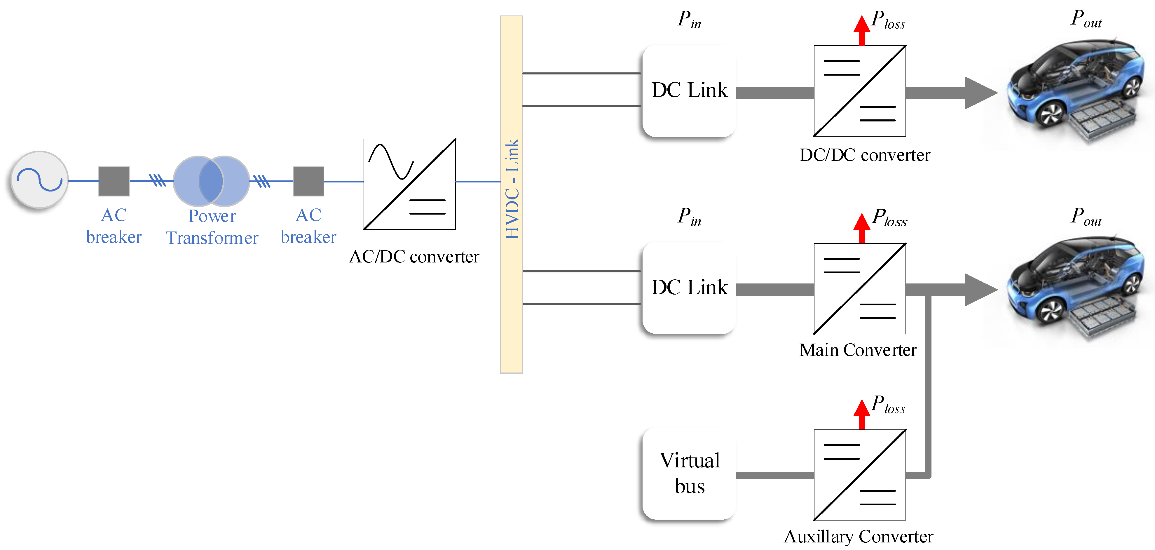
State-of-the-art DC fast chargers convert the three-phase AC voltage into the desired DC voltage in two stages: an AC/DC rectification stage that converts the three-phase mains into intermediate DC voltage followed by a DC/DC stage which converts the intermediate DC voltage into a controlled DC voltage fed to the EV battery as portrayed in
Figure 1.
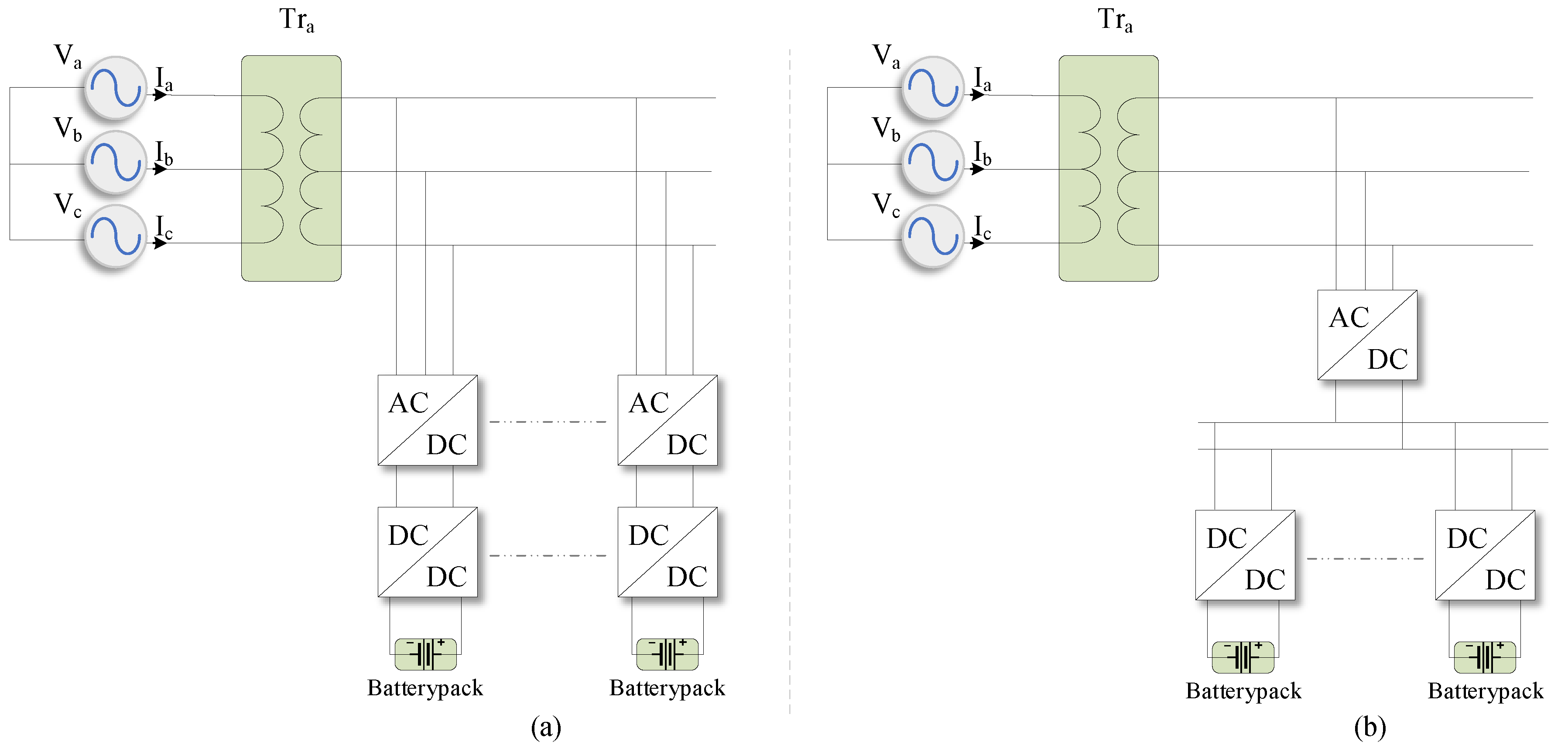
The AC-DC stage is not in the scope of this work. It will be assumed to be a conventional three-phase medium voltage passive rectifier with AC isolation transformer at power line frequency providing the DC voltage source suitable for the station, where the DC-DC charging stage is responsible for power control. Thus DC-DC converters are the main focus of this work. Conventionally, an offboard charger with multi-port charging slots is constructed in a way that shares either a common AC link or a common DC link as shown in
Figure 2.
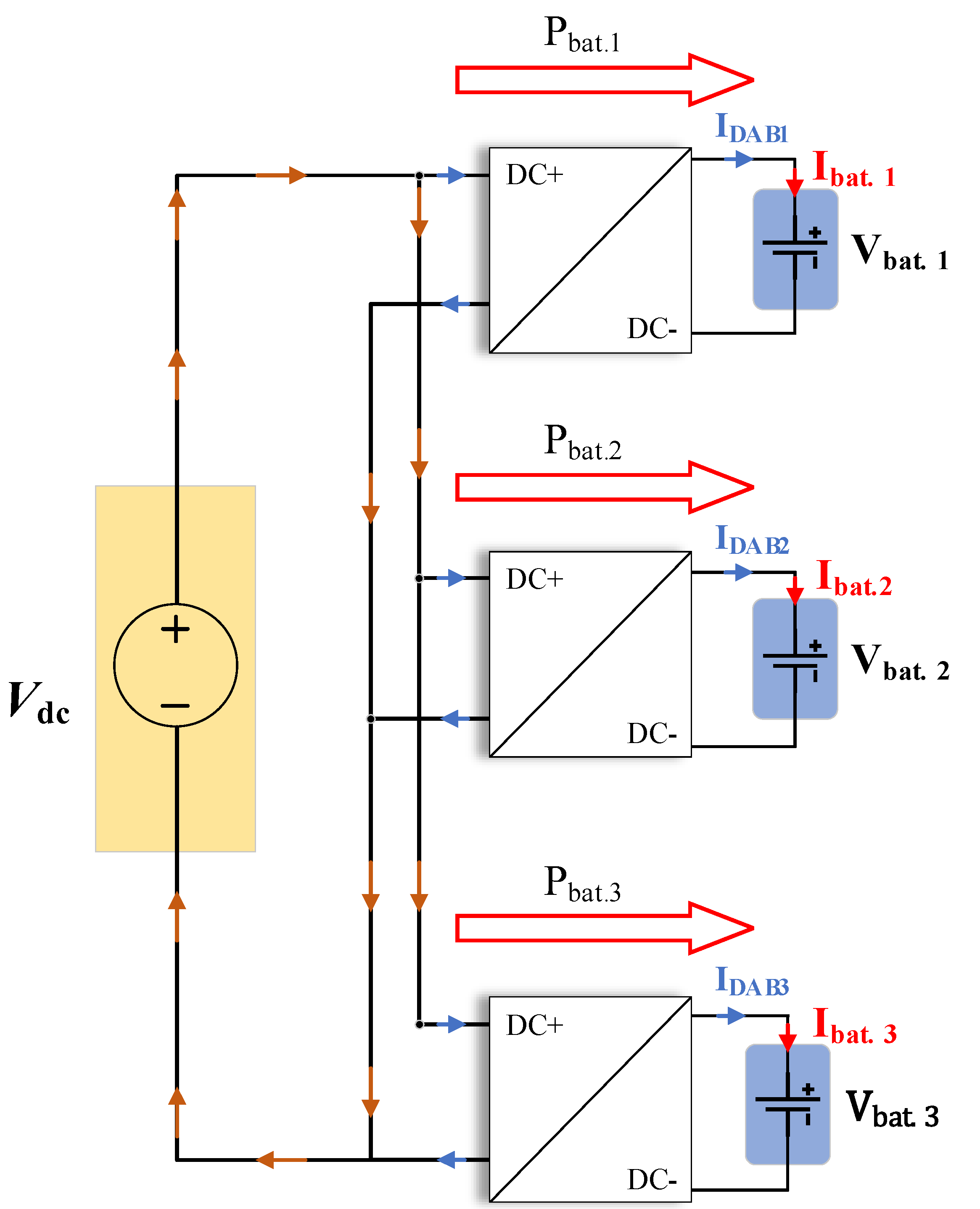
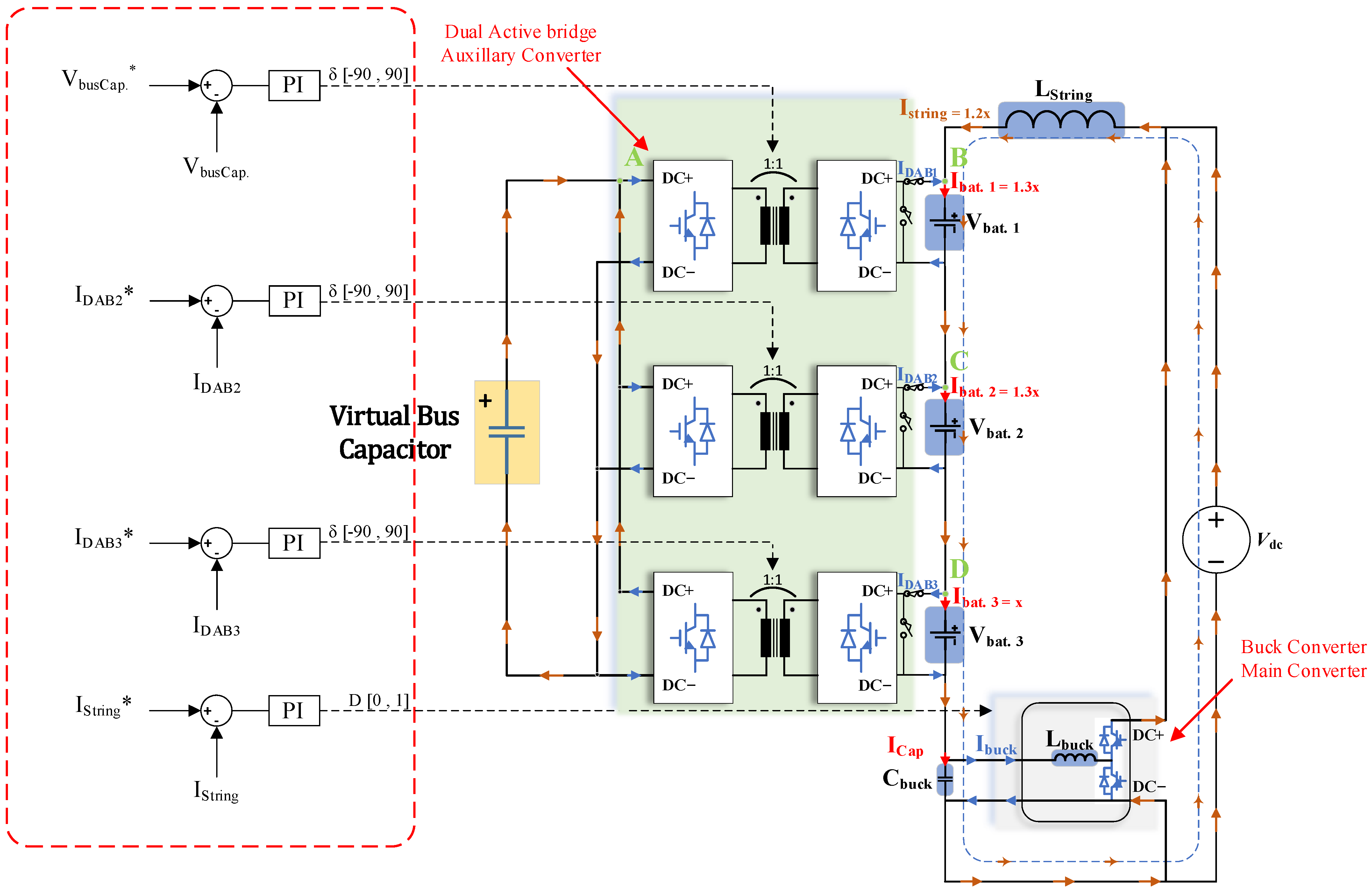
The proposed architecture relies on the concept of partial power processing, where a part of the load power is supplied via converters designed at a partial power rating. In the proposed system, the load power flows in two loops: outer and inner loops. The outer loop is responsible for transferring the bulk power to the battery, while the inner loop is controlling the auxiliary power. Since the proposed system provides charging to more than one battery simultaneously, each battery is interfaced to an auxiliary converter responsible for the partial power flow thus the number of auxiliary DC-DC converters is equal to the number of charging ports, while all the ports share the same outer loop. In the outer loop, all ports are connected in series where they share the same outer loop current (string current).
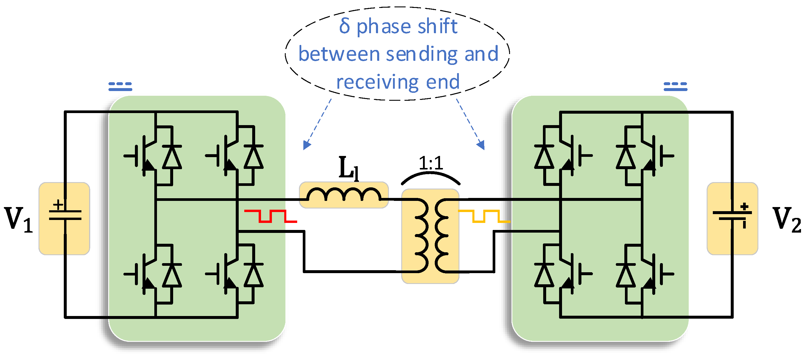
The key component of the DC charging stage is the DC-DC converter itself. A dual active bridge (
DAB), as shown in
Figure 3 has been selected as the auxiliary DC-DC converter because it exhibits the advantages of soft-switching, which has been widely investigated in [
22,
23].
- 2.
Converters in the Proposed Topology
Moreover,
DABs normally operate at high switching frequencies resulting in the use of high-frequency transformers that are mainly characterized by low volume, lightweight and lower cost. Choosing these converters as the constituent modules of the charging stage can ensure high efficiency, in addition to achieving bi-directional power flow, making it an ideal candidate in the experimental set-up discussed later in
Section 5. As illustrated in
Figure 4, the architecture consists of two types of DC converters: the
main converter in the outer loop and the auxiliary converters interfaced to the batteries. It should be pointed out that the proposed topology can be practically realized using any two-port DC/DC converter for processing differential power; however, in this work,
DABs have been selected for the aforementioned features.
The left side of the
DABs are connected in parallel to a virtual bus capacitor, which is regulated at the nominal voltage value by one of the
DABs. The voltage must be kept regulated at the virtual bus capacitor to ensure that the voltage ratio between the
DAB two ports match the transformer turns ratio to prevent circulating current and increase
DAB efficiency; i.e.,
[
22].
DABs can be controlled by several strategies according to [
22]. In this paper, a single phase-shift (SPS) control technique for the
DABs is adopted which can realize, according to [
22], flexible power and voltage regulation by adjusting the phase shift angle
between the bridges’ output voltage on the transformer primary and secondary sides. Furthermore, a bi-directional buck converter is selected as the
main converter to carry the bulk power since it has minimum switching components and has a wide range of voltage gain while maintaining a high efficiency operation, both main and auxiliary.
- 3.
Differential power processing concept
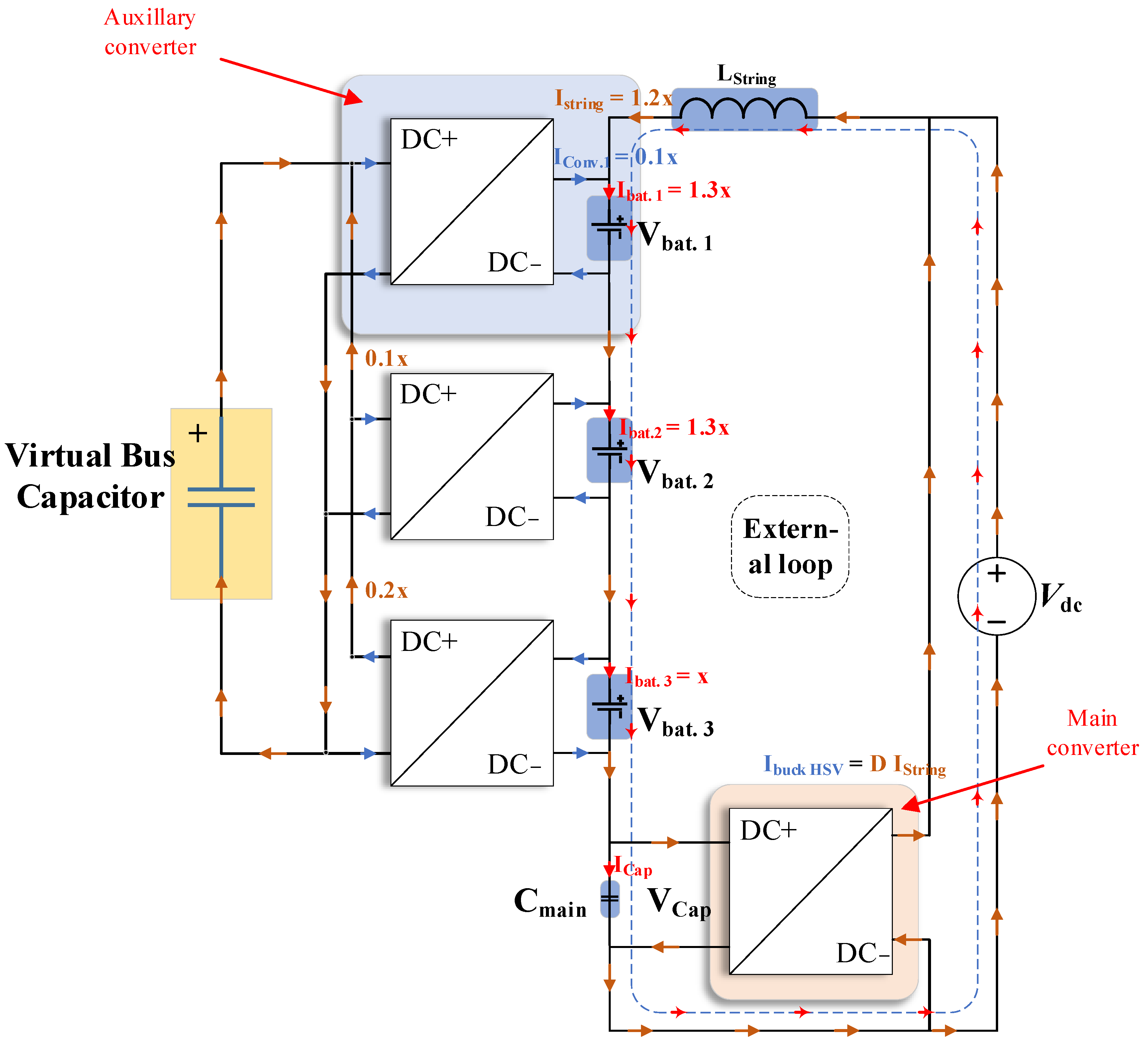
Figure 5 illustrates how the proposed architecture differs in the charging concept from the conventional topology in terms of power transfer.
Converters provide charging power for multiple output ports with minimum RMS input current due to the series connection; consequently, converters are rated to handle a small portion of the required power, which potentially optimizes system efficiency as well as installation and operational costs.
The bi-directional buck converter controls the outer loop (string) current by handling the voltage change in the series stack depending on how many slots are in service. The auxiliary DC/DC converters are designed at the voltage level of the EV battery while the bi-directional buck converter is to be designed at the rated voltage of the DC bus,
. Note that the scheme introduces a charging solution for three batteries being charged simultaneously, but that does not necessarily mean that such topology cannot be further expanded. The external loop supply voltage
must have a high voltage rating based on (1). Where
is the number of charging ports and
is the typical commercial EV battery voltage,
Consequently, it can be assumed that the system is expandable as long as a voltage source Vdc is sufficient for (1) to be satisfied. However, other limitations will arise during implementation; including:
Cost and size limitations of increasing the number of ports.
The available AC grid voltage that has been used to obtain the DC source, , (LV, MV, …etc).
Current limitation on the grid side in case of stepping up the voltage to a higher level to accommodate more charging ports.
- 4.
Brief Comparison between Proposed and Conventional Topologies
In conventional charging stations, a specific DC/DC converter is dedicated for each port with full power charging ratings as demonstrated in
Figure 6. Consequently, the installation and running cost of such a topology is dramatic. On the other hand, the proposed topology offers delivery of the same power with only a fraction of this power being processed by the auxiliary DC-DC converters, while the bulk power is being fed to the battery via the buck converter which has significantly lower total RMS current that results in lower conduction losses as will be clarified in
Section 4. With proper design, converters can be built to handle only
of the rated power, which, in return, improves installation and running cost, size of components being used as well as overall system efficiency.
3. Mathematical Analysis and Components Sizing
In this section, design equations are investigated and design parameters for the DC/DC converters are be specified.
- A.
Auxiliary DC-DC converter (Dual Active Bridge)
Based on [
22], the transmitted power in
DAB is given in (2).
The converter rated power is designed based on the rated voltages of the ports and a 30% of the rated power of the port, where is the transformer turns ratio, and are the voltages at the two ports of the DAB, is the switching frequency, is the AC link inductance and is the phase shift between the AC voltages generated by the two H—bridges of the DAB. The phase shift angle can take a positive or negative value according to power flow. From (2), it can be concluded that the controlled parameter is the phase shift angle , where all the remaining parameters are kept constant.
- B.
Bi-directional buck converter
The buck converter, responsible for string current regulation, is designed with ripple current of
of rated current and voltage ripple is kept at
. The buck converter is the
main converter in the proposed architecture. Additionally, it must be designed at the rated voltage of the system as it is directly connected to the main DC as illustrated in
Figure 7. Based on [
24],
is sized as explained in (3). The maximum duty reachable by the buck without shutting down the system is obtained in (4), where
is the maximum duty cycle,
is the rated input voltage,
is the ripple current and
is the switching frequency.
The converter input voltage, as shown in
Figure 7 and
Figure 8, is
which depends on the battery stacked in series based on (1). The maximum duty cycle is calculated according to a condition when all but one battery is connected. The system needs at least one battery to be connected to operate, otherwise, the system is offline. Therefore, the minimum buck voltage (
) should be designed as given:
- C.
Virtual DC link Capacitor
The virtual bus capacitor is connected to the primary side of all
DABs which is connected in parallel. Independent voltage regulation is done by one of the
DABs to ensure a fixed virtual bus voltage to achieve the voltage ratio of the
DABs near unity as aforementioned in the control section. Applying KCL at the virtual capacitor +ve terminal node A in
Figure 8, then
In a steady state, virtual bus capacitor current
thus,
where
is the current in the virtual bus capacitor. The sum of the
DAB currents should be equal to zero which assures that total power is balanced and processed at the
DAB inlet ports, where the virtual bus capacitor is only to maintain the voltage at the ports. Applying KCL at the nodes B, C and D in
Figure 8 results in:
As a result, adding (9)–(11) and for a general number of ports
leads to:
Therefore, to ensure that all the battery reference currents are maintained at the desired values especially at the
DAB that is responsible for the virtual bus voltage control, the reference string current (
) should be controlled at a value that satisfies
The input current on the other hand is slightly less than the string current and calculated as given in (14) by applying KCL at node A.
The sizing of the virtual bus capacitor should ensure a small voltage ripple. Applying KCL at the virtual bus capacitor depicted in
Figure 7, then
where
is the output current of the virtual bus capacitor. Based on the power equation given in (2).
where
is the virtual bus voltage ripples and
is the time difference, which can be substituted by the periodic time
. Thus, from (17), the value of the capacitor can be found according to
To correctly select the capacitance value, the phase shift
must be known. Therefore, the sizing is selected at the maximum
possible at all the
DABs; i.e., at
. In that case, the final capacitance formula is given by
- D.
String Inductance sizing
The string inductance here is designed as a current filter and to limit any sudden changes in the current during transients. Based on that, the string inductance is designed by studying the system during the transient instant.
Assuming a steady state condition with 2 ports running and applying KVL at the external loop
Assume that the current in one of the two running ports is equal to the rated current, ex: . Hence, the string current is equal to the average current of the two ports as proved in the manuscript.
In that case, the second port with less current is unplugged. Thus, new , yet still the buck voltage is at .
Thus, the objective here is to limit the current transient to be in range of of the rated current. This is designed at .
Applying KVL from (21) leads to:
Thus, the
is no longer equal to zero.
In our case, assume that and . Then, .
Unplugging the second port, the new string current is equal to the rated current. Applying (6), the string inductance required to limit the current in the desired range will be:
where
,
,
,
desired ripple ratio is 5%.
Sizing the inductance here was due to the fact that, we needed to establish an extreme case.
- E.
Power Losses Analysis
Since
DAB currents are reduced in the proposed topology, it can be proven that the efficiency is greatly increased in the case of differential power processing. Assuming that both the conventional and proposed topologies are considered from the same hardware components, the power loss in the conventional case can be obtained from:
where
is the MOSFET channel resistance. However, the switching losses in
DAB can be neglected due to zero-voltage switching. Therefore, (27) leads to
A numerical example of the charging currents is provided to get a rough idea about the loss analysis in case of the proposed system in
Figure 4 and compare it to the conventional architecture set forth in
Figure 6. Assume a scenario where,
As depicted in
Figure 7, it can be deduced in Equation (13) that the string current desired will be the average current and equals
. In this case, the auxiliary converter on the first and second battery will process
to be supplied to each battery, while the auxiliary converter connected to the third battery will process
to be processed by the converter and delivered to the converters connected to the first and second battery via the virtual bus capacitor. Additionally, the auxiliary converters used in the proposed system are
DABs as portrayed in
Figure 7. In order for
DAB to work properly at high efficiency, the voltage ratio must be equal to the transformer turns ratio; i.e:
Since DAB currents are reduced in the proposed topology, it can be proven that the efficiency is greatly increased in the case of differential power processing. Assuming that both the conventional and proposed topologies are considered from the same hardware components, the power loss in the conventional case can be calculated from Equation (28) for the system to be . On the other hand, from Equations (27)–(29) and since it can be concluded that power losses are reduced in case of the proposed topology leading to over all system loss of , which emphasizes the effective reduction in power losses in case of the proposed topology.
4. The Proposed Topology Control Technique
In this section, control strategies of each converter module are further investigated. According to what has been stated earlier in
Section 3, the adopted control strategy utilized with
DABs is SPS control, where the power flow magnitude and direction are regulated based on (2) [
25].
If a
DAB converter is not connected to an external car, all the gating to the
DAB MOSFETS are inhibited and the output terminals will be shorted by a mechanical limit switch that is interlocked with the EV connector to ensure continuation of current in the external loop by bypassing the open port. The buck converter should compensate the voltage of the outer loop, resulting in an uninterruptible operation in the system as depicted in
Figure 8. Additionally, in case of an open circuit fault in one of the auxiliary converters, the limit switch will ensure continuation of service at the remaining port in the same fashion. The bi-directional buck converter in
Figure 7 and
Figure 8 is used to regulate the string current and keeps it constant at the average current value of the batteries being charged as proven in (13). This is realized by regulating the buck voltage according to the duty cycle in such a manner that, if the string current should be increased, the output voltage and, hence, the duty
decreases and vice versa. The relation between the buck duty cycle and the system parameters can simply be explained using KVL as explained in Equation (32).
From Equation (32), it can be concluded that should any battery be disconnected, the buck converter will compensate the voltage by increasing the duty cycle and maintain the string current to the new average value of the connected batteries. The remaining converters are responsible for the charging current regulation. Consequently, the controlled parameter at each
DAB is the battery charging current based on Equation (33).
According to Equation (33), the DC converter processes only a fraction of the current; depending on the battery charging demand, the
will be
(supplying power) or
(receiving power). Assume a scenario where
, as represented in
Figure 8. It can be deduced in (
13) that the string current desired will be the average current and equals to
. In this case, the
DAB converter on the converter on the first and second battery will process
to be supplied to each battery, while the
DAB connected to the third battery will process
to be processed by the converter and delivered to the
DABs connected to first and second battery via the virtual bus capacitor. Furthermore, as aforementioned, for
DAB to work properly at high efficiency, the voltage ratio must be equal to the transformer turns ratio. For that reason, the virtual bus capacitor voltage must be maintained constant, and this is realized by one of the
DABs. The controller of the
DABs regulates the phase-shift angle between the two bridges according to the
flowing in the converter. The control block diagram is depicted in
Figure 8, where the first
DAB is responsible for the virtual bus voltage control, while the rest of the
DABs are controlled to achieve the desired current value of their corresponding batteries. The control parameter in case of the
DABs is the phase shift angle between the two bridges,
, ranging from
. Finally, the buck is used to control the string current to the average values of the desired battery currents. It is worth noting that the first battery current is not controlled by the corresponding
DAB, because the corresponding
DAB is responsible for the virtual bus voltage control.
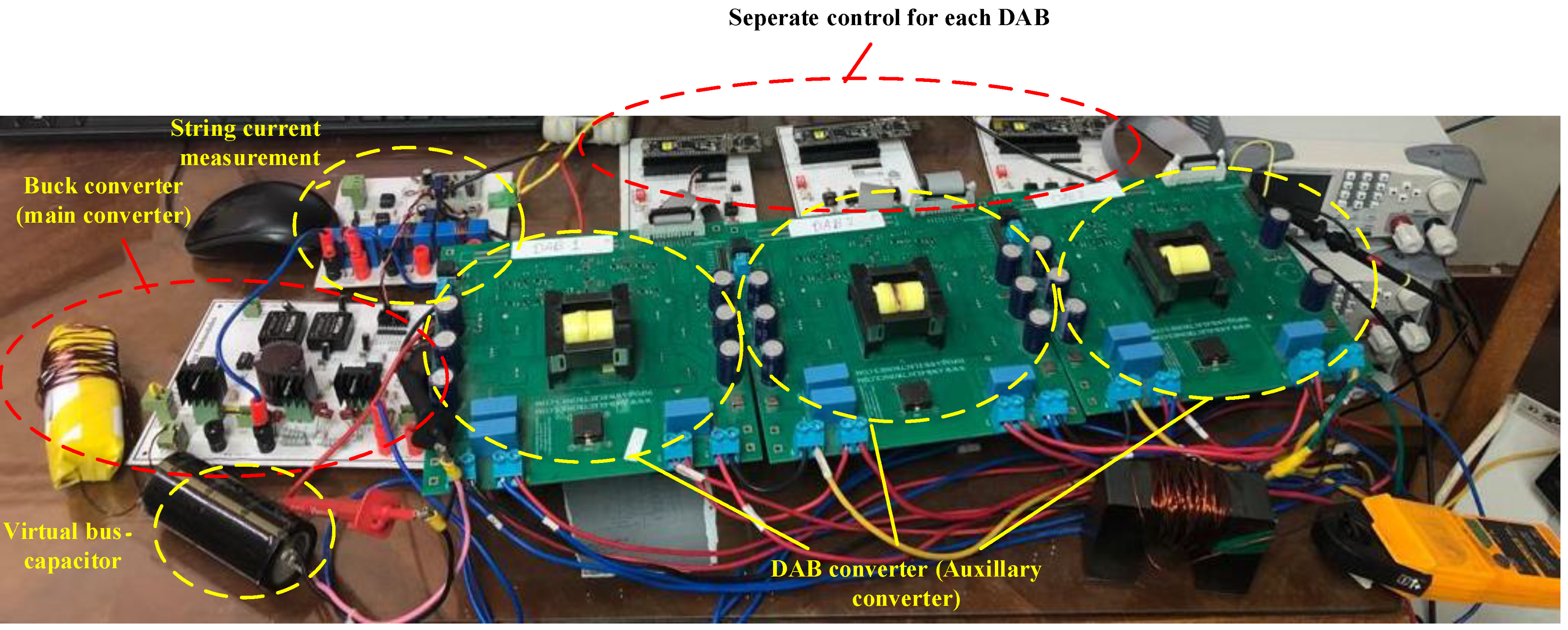
5. Experimental Hardware Validation
In this section,
Figure 9 shows a scaled-down laboratory experimental setup that is used to experimentally validate the proposed architecture under different test conditions. We compare the proposed system to the conventional architecture, which is composed of the same types of converters, highlighting the advantages of the proposed system over the conventional one.
The objective in this section is to compare the proposed architecture and conventional topology under different testing conditions.
- A.
A look into the set-up
The experimental set-up has been designed as a proof of concept with most of the parameters being scalable for real-life design. The PSoC Arm-based controller has been utilized as the main controller for the prototype. Modular control has been realized in which each power converter module is separately controlled with a dedicated PSoC controller, which enhances system reliability.
In order to guarantee highly efficient DAB performance, soft switching for the converter must be ensured; additionally, converter bridges constituted of highly efficient MOSFETS with low and high switching frequeny should be considered. In our set-up, SiC switches with high switching frequency capability are provided. Moreover, the gate driver modules that have been used operate efficiently at high switching frequencies with hardware dead bands that optimize the bridge output signals with the least disturbance possible at high switching frequency operation. DABs have been designed to handle only 30% of the battery power providing a high efficiency improvement. In the set-up, the DAB rated power is designed at at max phase shift of with a switching frequency of . The isolation transformer is designed individually with turns ratio , voltage rating of and leakage inductance almost equal to zero. Substituting in (3), the required inductance is . The buck converter is designed at a switching frequency of and designed at . The buck converter inductance is designed at the maximum reachable duty cycle based on (4) which is found to be 0.75. Hence, the buck inductance is calculated from (3) with current ripples 0.5 A (10%) to be 1.8 .
Selection of the DC virtual bus capacitor, based on (19), depends on the desired voltage ripple. In our case, the voltage ripple is designed at of the voltage resulting in a virtual bus capacitance of In the set-up, is chosen.
The power supply used to charge the batteries is rated and . The system has been investigated with power supplies connected to resistive loads in parallel that model battery behavior during charging with constant current.
- B.
System parameters
The system parameters as well as controller parameters applied to the system are summarized in
Table 1.
DAB design parameters are shown in
Table 2.
- C.
Normal operation
To validate the efficiency benefits, the proposed topology is compared to the conventional architecture at three operating events: normal operating condition when batteries are charging at a desired reference current, at online load dynamic changing and at voltage build-up of the battery.
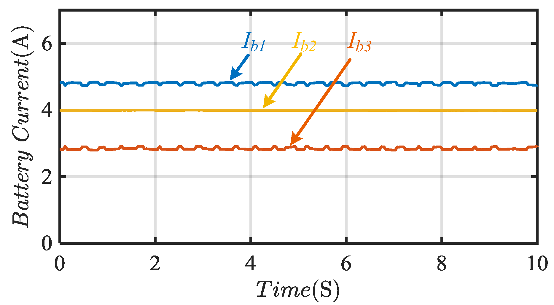
Case I Normal operation with three ports in service:
In this scenario, the normal operation of both topologies is investigated, and system currents and efficiencies are compared. In this case, three different charging ratings are selected;
, as depicted in
Figure 10. In order to regulate the string current at the average current of the connected ports (13), the buck converter is required to regulate the voltage at the series capacitor. It can be noticed that both
, and
are imposed with ripples, while
has less ripples. This is because the reference current at the second port is equal to the string current,
, which means that the current supplied by the auxiliary converter connected to port 2,
. On the other hand, currents processed by DAB1 and DAB3 are non-zero which imposes ripples at the port current, from (9)–(11).
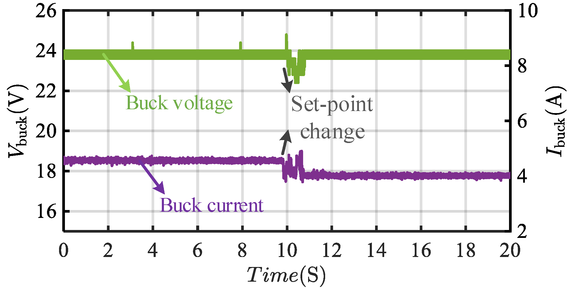
Based on (32), the buck voltage output will be maintained around
in that case.
Figure 11 highlights buck output voltage and current. It can be noticed that the buck converter succeeds in controlling the string current to the batteries at an average value of
. Voltage and current ripples are kept within the design range for both at
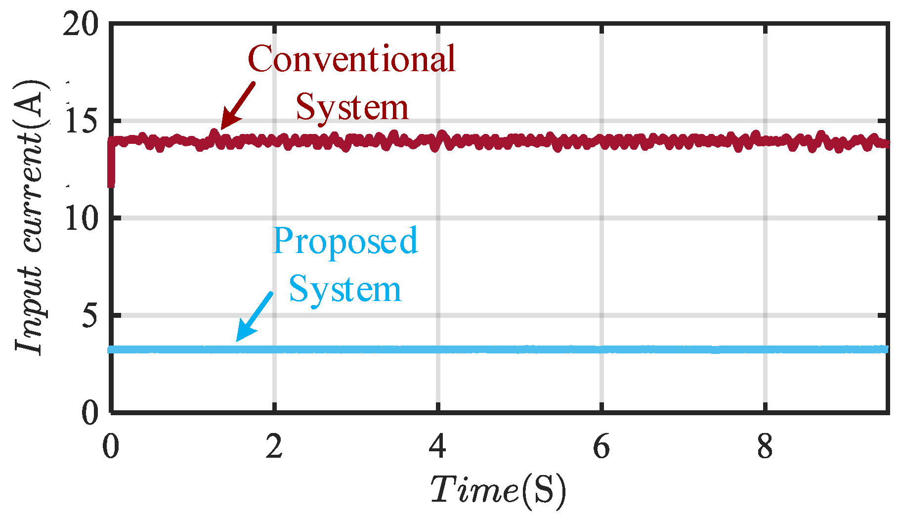
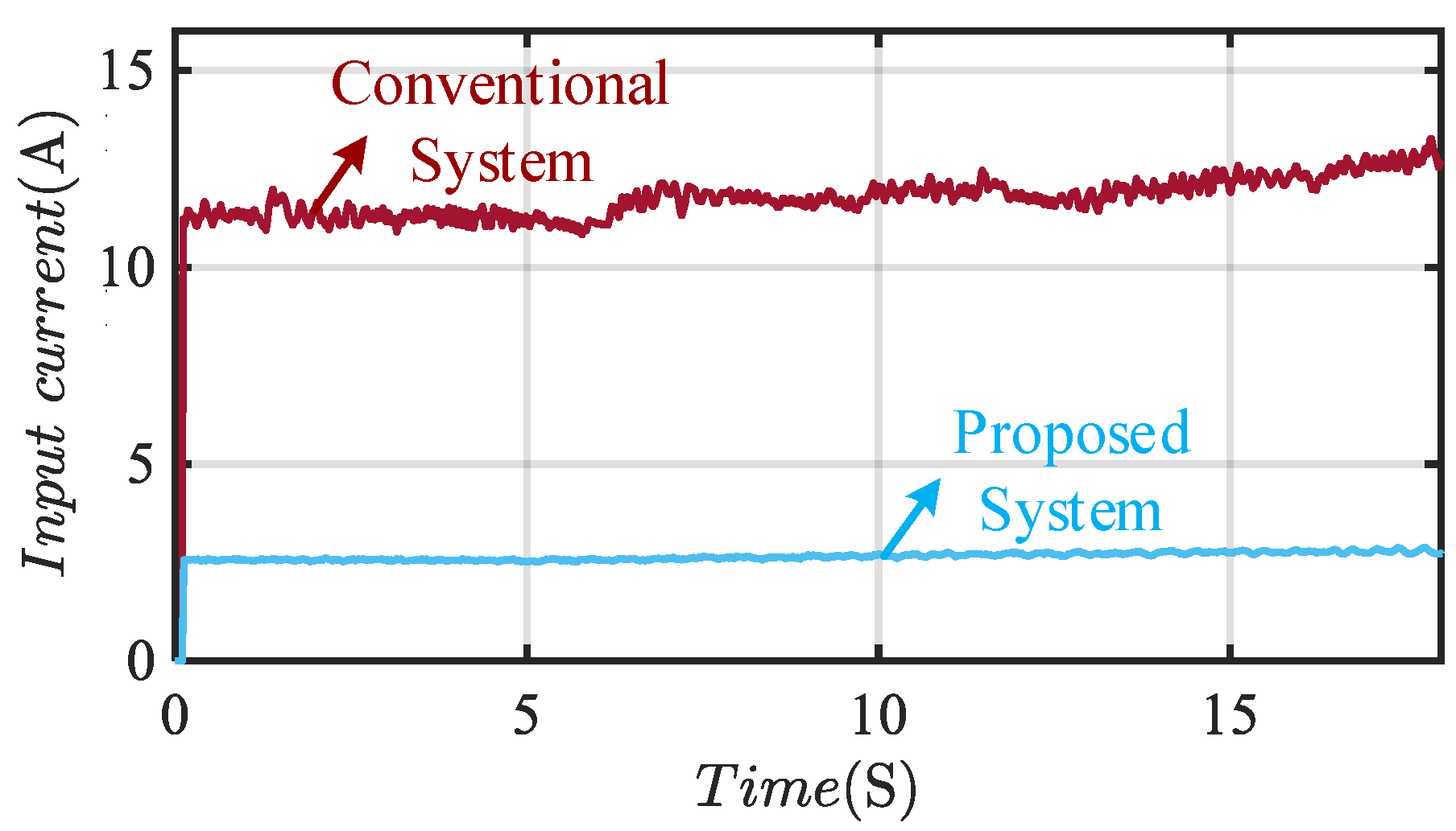
. The current withdrawn from the supply in case of the proposed configuration is much lower as compared to the conventional topology.
Figure 12 depicts the major difference between the input current in both cases. In the case of conventional configuration, the input current is ideally the summation of the all the battery currents connected. But since the system is non-ideal, the system input current is expected to be higher. On the other hand, the input current of the proposed topology is expected to be less than the string current.
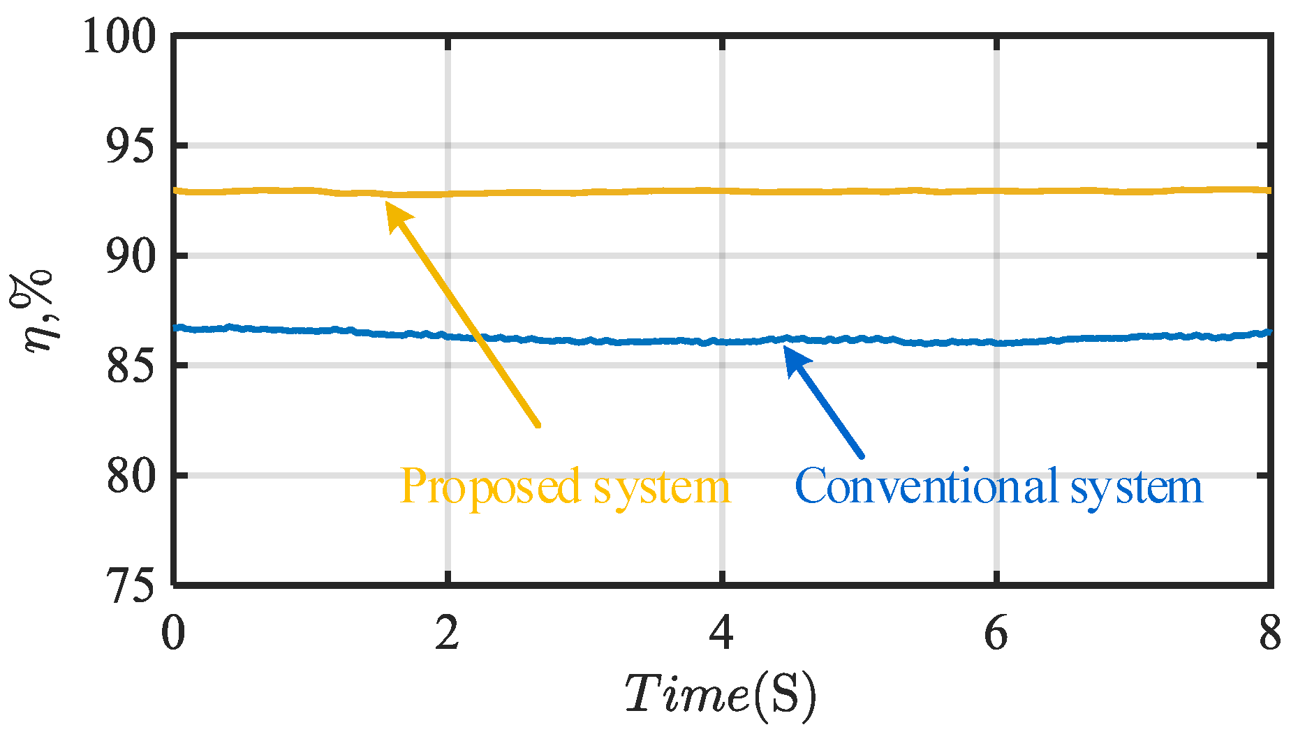
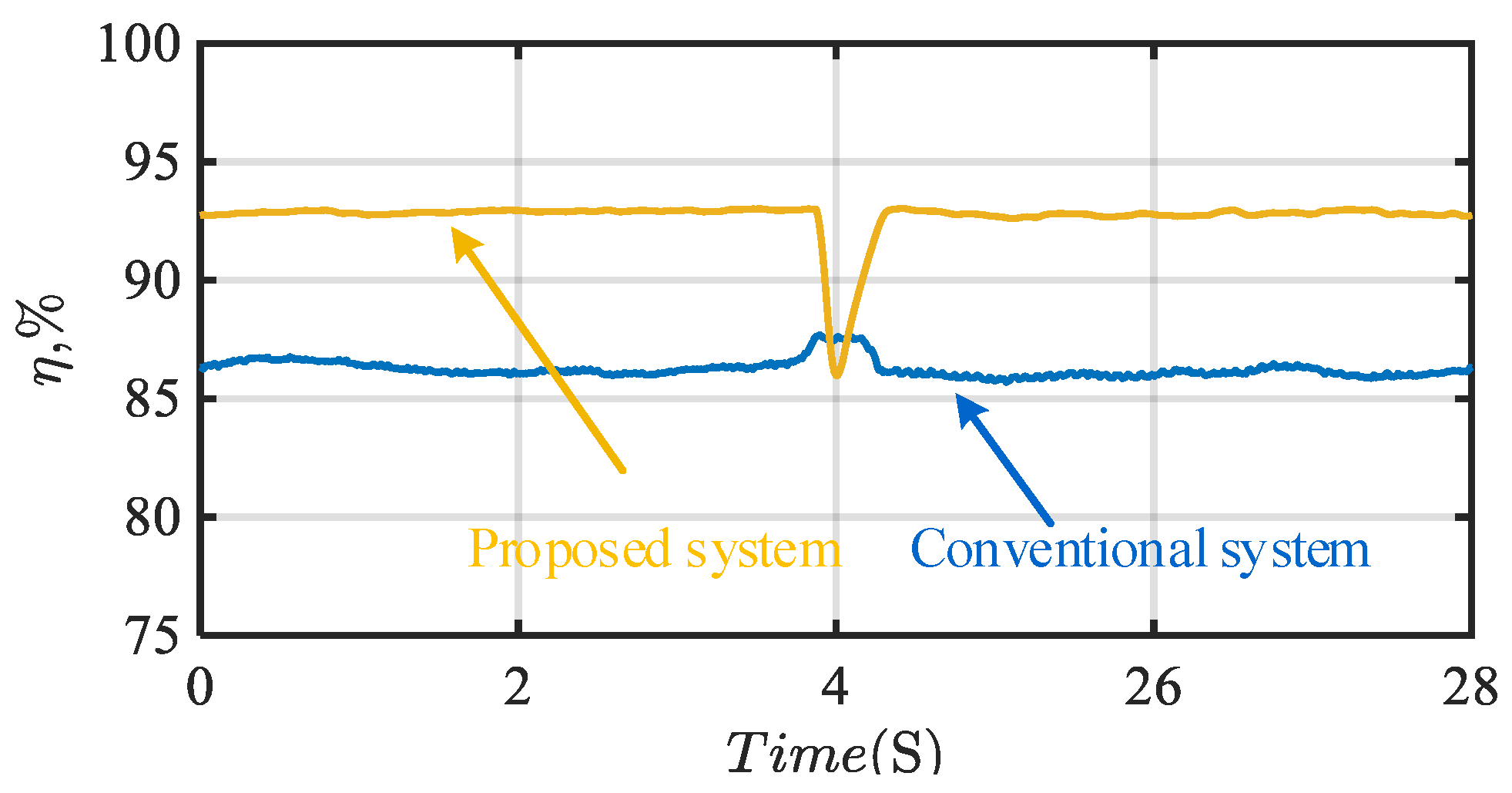
System efficiencies are compared and illustrated in
Figure 13.
Based on the readings illustrated in
Figure 12 and
Figure 13, the proposed architecture has better system efficiency for same charging power. The power charging unit has been rated to handle only about 30% of the battery power providing an efficiency improvement of about 7% as compared to the conventional scheme that must be rated to handle the full charging power.
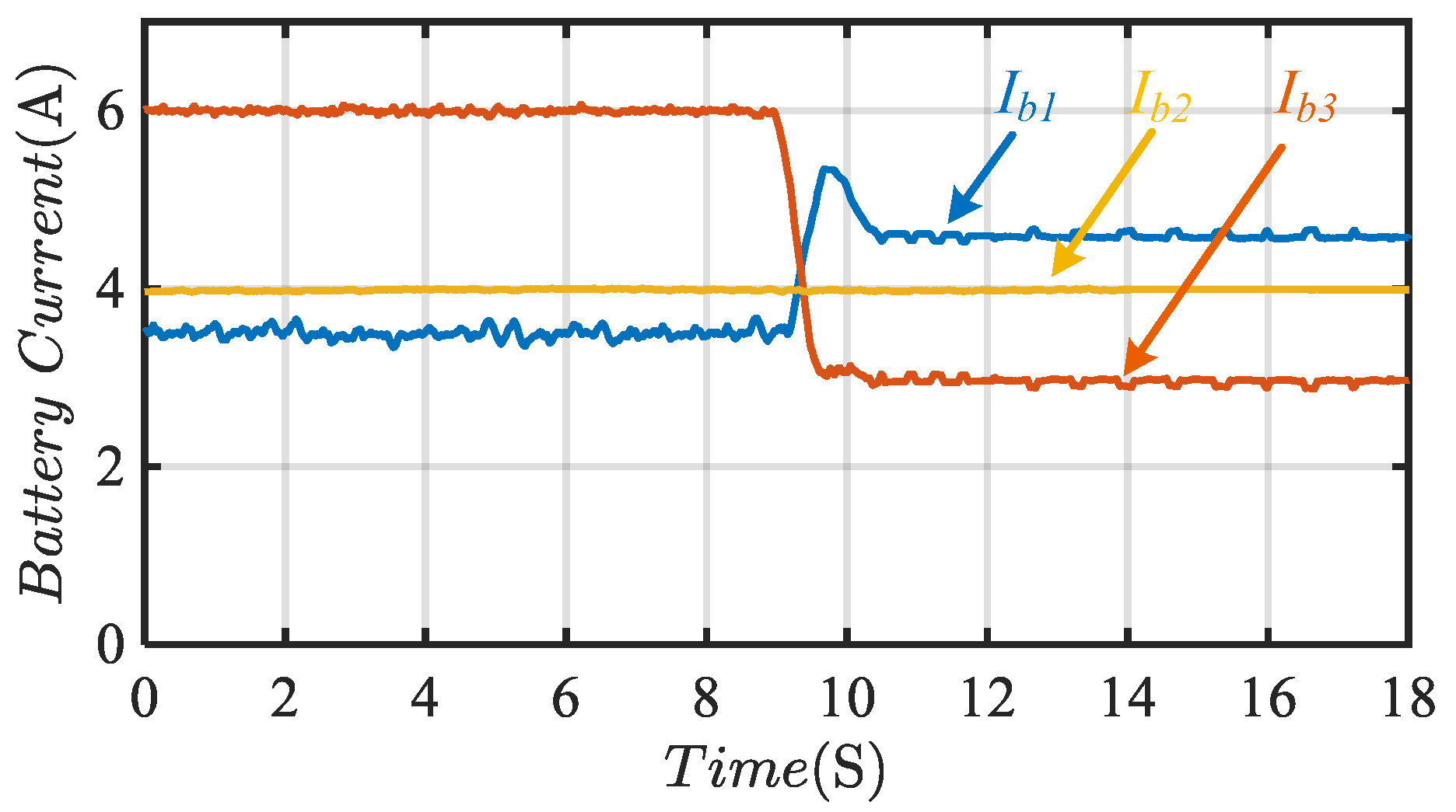
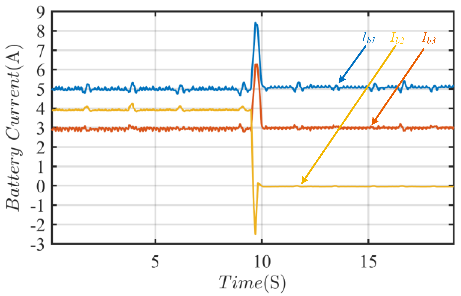
Case II Dynamic change of charging power:
In this case, the system dynamics are further investigated via online change of the power delivered to the batteries. This is achieved by changing the set point of battery currents
. It can be noticed in
Figure 14 that for battery 1 and 3, the current has been changed;
reference value has been changed from
to
and
reference value has been changed from
to 4.
.
The buck converter output characteristics are as illustrated in
Figure 15 noting that the buck voltage exhibits a transient behavior at the instant of the step change to control the string current to the new average value.
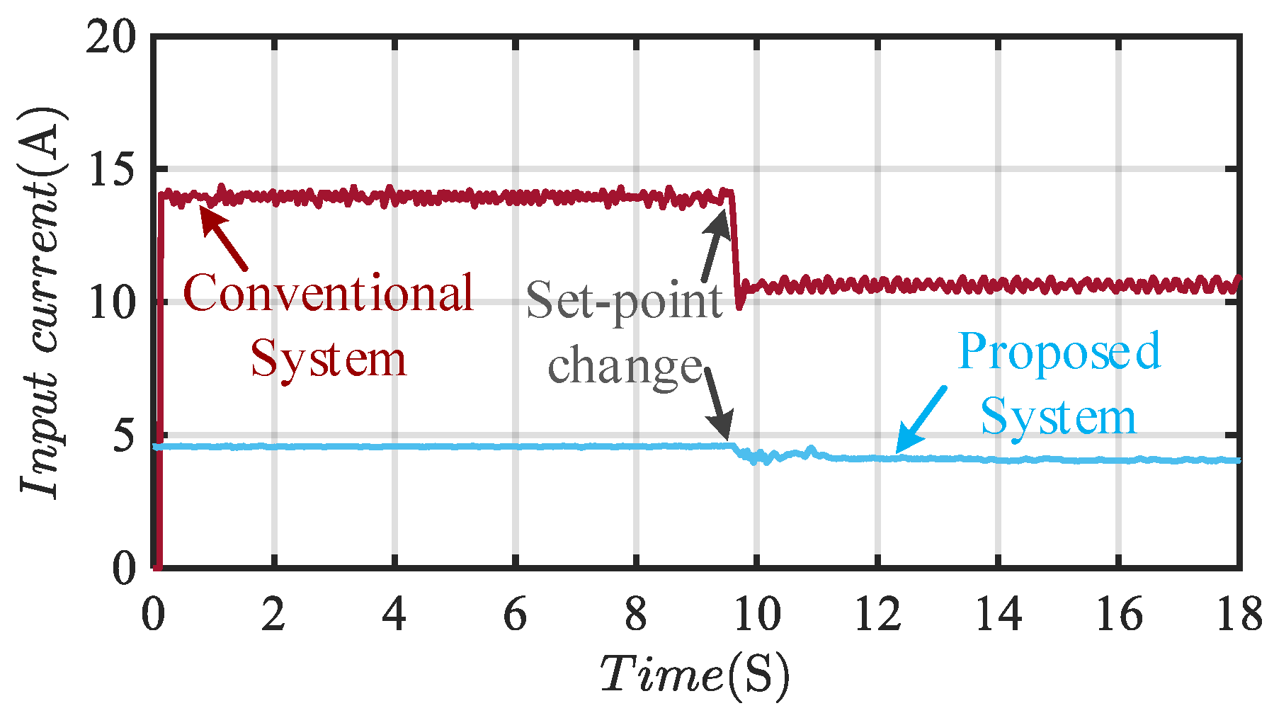
Input current is compared in both cases as shown in
Figure 16. In the case of the conventional configuration, the input current is the summation of battery currents, which accounts for the high current level. On the other hand, in the case of the proposed architecture, the reference has changed to the new average current with minimum change in the input current. This highlights the system stability with load variation unlike the conventional system which undergoes significant variation in the input current. Hence, the input current in case of the proposed system is more stable and does not show much change.
Case III Simulating battery performance:
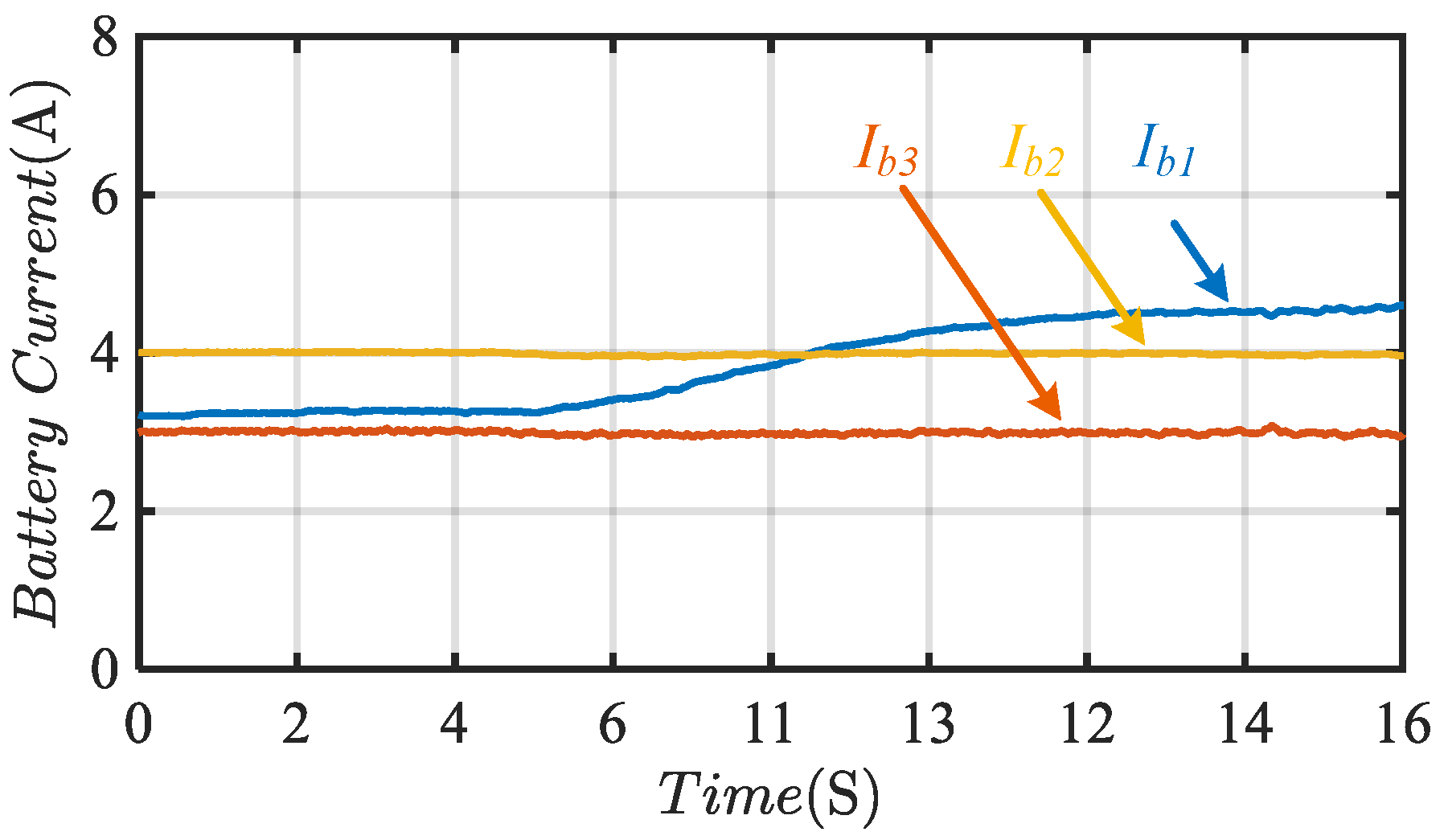
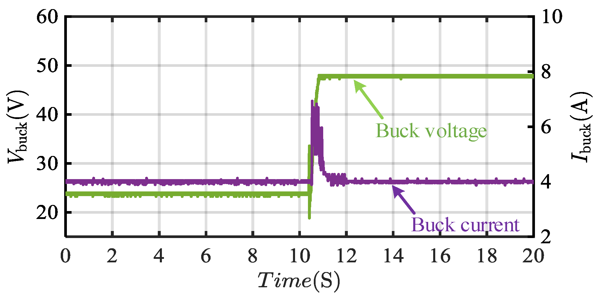
In this case, battery charging is simulated to investigate system behavior with load voltage rise.
Figure 17 shows the charging currents of the batteries where the currents at port 2 and port 3 are successfully maintained at their desired value. On the other hand, the current flow at the first port is changing because the corresponding DAB is to control the virtual bus capacitor voltage (refer to
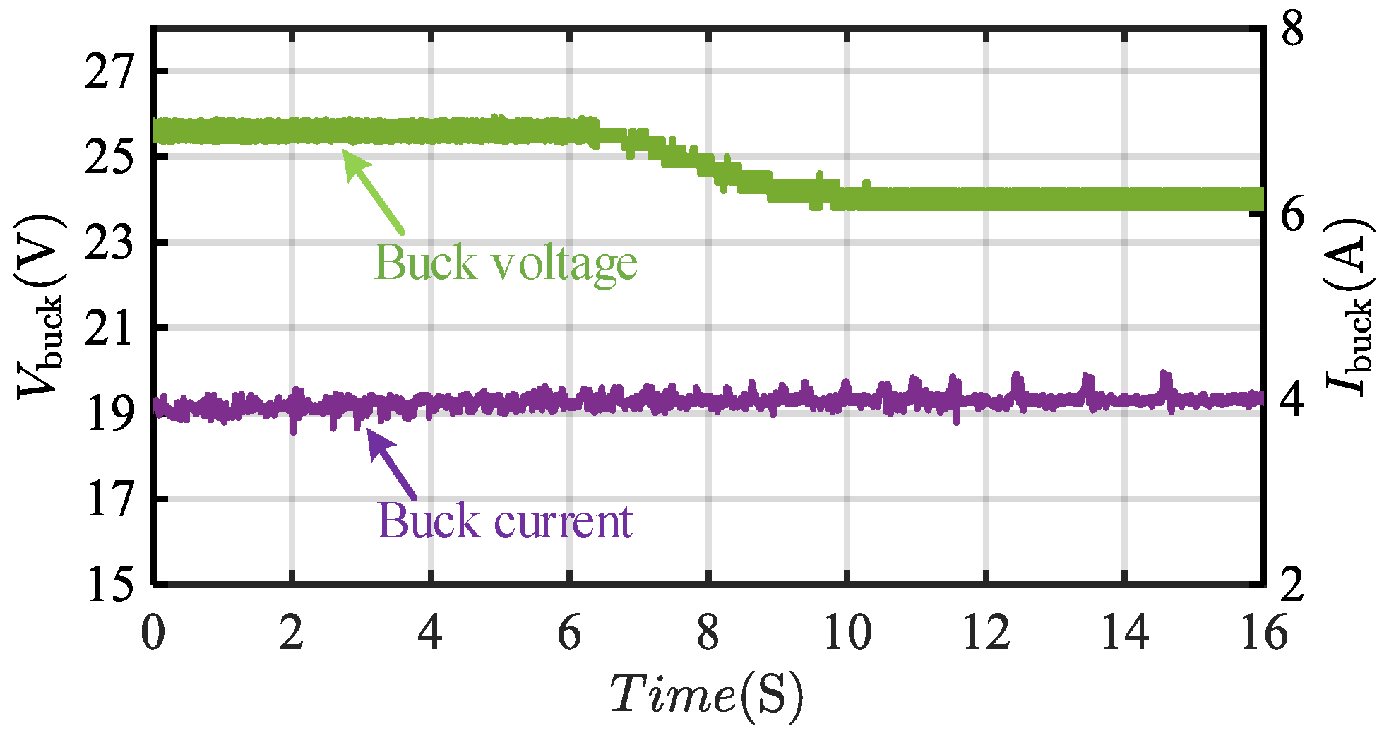
Figure 7). Hence, the output current at port 1 has increased to maintain the virtual bus voltage constant. When the battery is being charged, the battery voltage increases. The buck converter output voltage reduces concurrently to maintain the current in the outer loop (string current) constant as shown in
Figure 18. Input currents in the case of the proposed and conventional system are presented in
Figure 19.
- D.
Fault tolerance
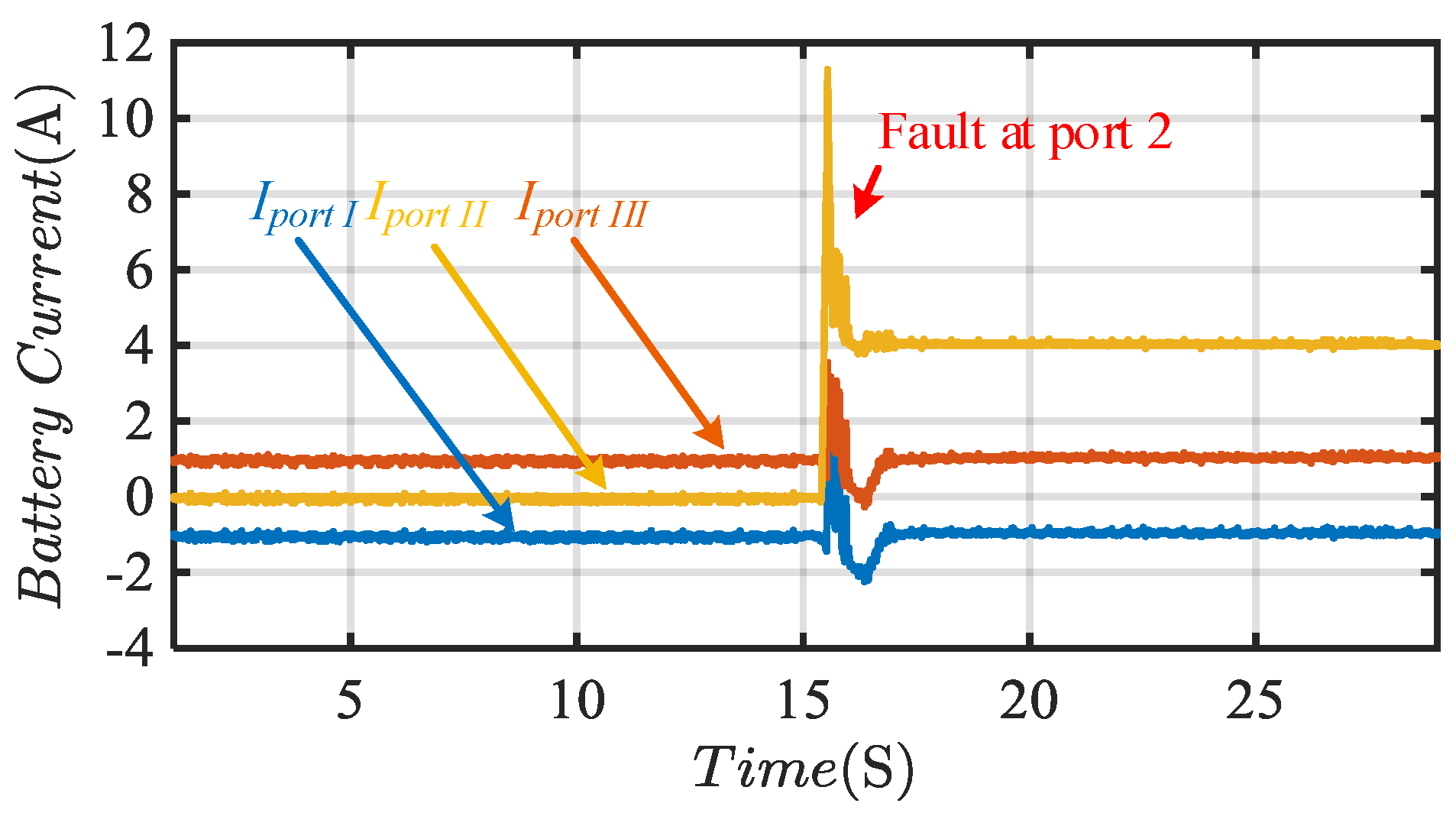
In this section, the system is studied under a fault case where a short circuit occurs at one of the batteries without power interruption to the remaining batteries. The fault can be detected by means of monitoring the voltage level to prevent operation of the faulted port; however, this is not implemented in the software in order to investigate the fault tolerance of the system. A fault scenario is implemented on port 2 as shown in
Figure 20. At the instant of the fault, the current at the faulted port reaches zero, while the output current of the DAB ports increases instantenously. Due to the current control in the string as well as the remaining ports, the DAB current at the faulted port output will reach zero, yet the current at the port node (where the DAB and the string current meet) will be equal to the string current based on Equation (33), as can be depicted in
Figure 21, which implies steady system operation and fault tolerance capability of the converter. The reason behind the current stability at the faulted port is that the buck converter output voltage has increased from
to compensate for the voltage reduction due to the faulted port and to maintain the string current at the new average value based on Equation (13). As a result, the string current which is the buck current is regulated at the reference value as shown in
Figure 22 because the average current of the remaining ports is kept unchanged after port II termination.
Comparison between the two systems based on the system efficiency is illustrated in
Figure 23. It can be brought out that, with the proposed topology, efficiency is kept at the maximum attainable value. Moreover, since such a topology is expandable, with more batteries being plugged in or increasing the number of charging ports, the efficiency remains almost unchanged. Thus, the efficiency comparison has been made emphasizing that the system has better performance in case of proposed architecture.


 ,
, 


