Article

Thermal Assessment of Dielectric Microspacer Technology Using an Advanced Three-Dimensional Simulation Model

by
Myrto Zeneli
1,2,*,
Alessandro Bellucci
3,
Gianfranco Sabbatella
4,
Maria Fotopoulou
1,
Vasilis Apostolopoulos
1,
Panagiotis Stamatopoulos
1,
Daniele M. Trucchi
3,
Aristeidis Nikolopoulos
1 and
Dimitrios Rakopoulos
1
1
Chemical Process and Energy Resources Institute, Centre for Research and Technology Hellas (CERTH), 52 Egialias Str., Marousi, GR-15125 Athens, Greece
2
Laboratory of Steam Boilers and Thermal Plants, National Technical University of Athens (NTUA), 9 Heroon Polytechniou Str., Zografou, GR-15780 Athens, Greece
3
Institute of Structure of Matter ISM-CNR—DiaTHEMA Lab, Via Salaria km 29.300, Monterotondo, 00015 Rome, Italy
4
IONVAC—Ionvac Process Srl., Viale Anchise 24/25, Pomezia, 00040 Rome, Italy
*
Author to whom correspondence should be addressed.
Sustainability 2023, 15(3), 1786; https://doi.org/10.3390/su15031786
Submission received: 24 November 2022 / Revised: 2 January 2023 / Accepted: 4 January 2023 / Published: 17 January 2023
(This article belongs to the Special Issue Energy Technology and Sustainable Energy Systems)

Abstract

:
Dielectric microspacers (DMS) are a novel micro-technology that can be used to achieve a fixed micron/sub-micron gap distance between two separated surfaces, such as the emitter (cathode) and the PV cell (anode) of a near-field thermophotovoltaic converter (TPV). One of the system’s challenges is the flow of undesirable excess thermal energy from the cathode to the anode that might cause the PV cell to overheat. This work investigates the possibility of integrating this technology into a hybrid thermionic-photovoltaic (TIPV) converter operating at ultra-high temperatures (>1000 °C) without any risk of collector’s overheating, which might lead to its mechanical failure. A steady-state 3-D CFD model was developed in Fluent v17.1 solver to assess the system’s thermal behavior when the two electrodes were separated by a distance of 8–10 μm. The heat transfer through conduction across the system components and the net photon/electron flux between the two electrodes were simulated. Different cathode temperatures within the range of 1500–2500 K and various DMS shapes (capillary, cylindrical), patterns (e.g., ring-shaped) and sizes were studied. Results show that thermal performance is not affected by the DMS pattern, even for thermal conductivities of 80 W/(m·K), whereas the possibility of mechanical failure is considerable for Tcathode > 2000 K.

1. Introduction

1.1. General Context

The optimal development and implementation of solid-state energy converters, such as thermophotovoltaic (TPVs), thermionic (TI), photon-enhanced thermionic (PETE) and hybrid thermionic-photovoltaic (TIPV) converters, constitutes a research field that has gained attention over the past few years due to their contribution in the current energy transition [1,2,3,4]. More specifically, this kind of novel energy converter may increase the power output of renewable energy technologies and enhance the sustainability of the energy sector by achieving conversion efficiencies higher than 40% [5]. However, due to their low technological readiness level, there are still open issues regarding their optimal design, the involved materials and their thermal-electrical properties, the inappropriate selection of which might cause several technical problems, e.g., the overheating of the anode, which may result in extra losses in the conversion efficiency, degradation of materials, micro-cracks, strength depletion, etc. [6]. Therefore, special attention is paid to various aspects to increase their operating performance and avoid their mechanical failure, ranging from the optimization of the cooling system used to remove any excess thermal heat up to the potential use of single-layer or multi-junction layers, as well as the design of a sub-micron vacuum gap between the anode and cathode.
Several research papers focus on the simulation of these novel converters. For instance, the authors of [7] present a 1D numerical model for the simulation of PN junctions in thermophotovoltaics and analyze their operating conditions and the involved semiconductors. From another aspect, the optimal cooling method of a hybrid TIPV converter was studied in [8], for the purpose of which a copper plate heat spreader was utilized and evaluated through experimental investigation, as well as computational fluid dynamic (CFD) simulations. Furthermore, in [9], a TIPV converter comprising In0.53Ga0.47As PV anodes was experimentally demonstrated. The demonstrated converter provided an increased output voltage, up to ~0.5 V higher than the respective/reference thermionic energy converter (TEC) made of the same electrode materials, operating under similar conditions, i.e., in the 1190–1420 °C cathode temperature range. The TIPV concept was also demonstrated for a three-terminal device, with a maximum output power of 0.13 W/cm2 at 1400 °C [10]. Other researchers [11] aimed at enhancing the power density of TIPV converters by applying a graphene-on-semiconductor heterojunction anode to a TIPV converter and managed to increase the open-circuit voltage from ~0.9 to ~1.9 V in comparison with an identical configuration without the graphene layer. The application of an ultra-thin and small gap between the hot and the cold electrode of solid-state energy converters, by using dielectric materials as insulators, widely known as spacers, offers great potential to improve the conversion efficiency [12]. In this context, interelectrode spacers play a key role in achieving ultra-high thermal and electrical insulation at high temperatures and constitute an effervescent research topic both for TI and TPV devices.
Microscale and nanoscale vacuum gaps are used to minimize conduction losses and allow higher power outputs [13,14]. The micron-scale inter-electrode insulation is usually based on novel thin film materials called dielectric micro-spacers (DMS) [5,15]. In particular, research in the field has shown that implementing a sub-10-μm gap between the electrodes can minimize space-charge losses, which in turn, can increase the absolute efficiency up to 35% [16]. A good illustration of this is the design, fabrication and compression testing of thin-film alumina-based spacers by [15]. Based on alternative design considerations, as well as finite-element modeling simulation and optimization, the authors created a high-thermal insulated spacer demonstrating mechanically robust 3–8 μm gaps. In another study [5], small vacuum gaps with a thickness ranging from 0.3 to 3 μm were achieved by using alumina and zirconia ceramic thin films as DMS. Additionally, 2D finite-element thermal simulation models were developed and also electrical measures were taken to examine how some geometrical aspects may affect the anode temperature, thus, optimizing the distribution and the structural and material properties of the DMS at high-temperatures. Recent evaluations of the ideal gaps are even lower than 1 μm down to 300 nm [17,18]. The authors of [13] developed micro-fabricated ceramic spacer films with a thickness of ~400 nm and high thermal resistance that narrow the available area (~1.25 cm2) for conductive losses. They demonstrated their use in a thermionic converter, achieving a temperature difference of approximately 350 K over a gap of ~2 μm. The design, fabrication and testing of the promising DMS was based on a 2D simulation and structural analysis of the materials, as well as experiments considering specific combinations of geometrical aspects and material mixtures. Hexagonally-patterned U-shaped channels were opted for in both [13,15] to limit the available heat transfer area.
Despite minimizing the gap distance to the micron/sub-micron-scale (gap sizes d < 10 μm), which is essential for eliminating space charge losses, the prospect of achieving mass-producible and fixed-form gap-maintaining spacers is a multi-challenging issue pertaining to material, structural, mechanical and thermal aspects [19]. DMS should be sufficiently thermally and electrically insulated over the entire arranged surface and thin enough to minimize the thermal conductance; mechanically robust and strong enough to prevent thermal or electrical shorting due to the spacer bending, cracking or collapsing; chemically and mechanically stable at high temperatures; thermally resistant to reduce parasitic conductive losses, and easily installable [5,12,15]. To address these challenges, further research on the aforementioned aspects should focus on the optimization of DMS and improvement in the performance of semiconductor devices under various DMS patterns, different operating conditions and material properties. Due to the fact that experimental methods are costly and time consuming, the optimization and scale-down approach requirements of DMS can be investigated by simulation models considering the material properties and thermal behavior of DMS under various design considerations, performance targets and manufacturing constraints.
In this context, the aim of this paper is to examine and assess the thermal and mechanical potential of DMS technology when integrated into TIPV converters. For this purpose, a critical analysis of its thermal behavior for a wide temperature range is carried out in order to figure out the effects of the physical properties on the overall system thermal and mechanical performance levels when different operational and structural schemes are considered. In particular, the outcomes and perspectives that will arise from the current research can pave the way for the establishment of commonly acceptable operational thermal resistance and stability standards in this type of system and come closer to the realization of sustainable DMS manufacturing. Even though most studies in the literature focus either on optimizing the DMS gap for solar cell efficiency purposes or on improving DMS structural dynamics in the whole system, or even projects dealing with fabricating and testing DMS in real-life environments, such as PROME3THE2US2 [20], a holistic modeling approach that introduces the applicability of the specific systems for validation in various design and operational conditions, as well as uniformity and sensitivity analysis of the material properties, and incorporates the thermal effects on mechanical strength was lacking; it is presented in this current study.
To this end, a detailed three-dimensional (3D) CFD simulation model for the thermal assessment and parametric study of DMS under different operating conditions and various structural/geometrical patterns was developed. The model assesses the thermal behavior of DMS and allows screening for hot spot areas considering the heat transfer process occurring within a novel Cathode-DMS-PV anode (TIPV) system. Both a simplified and a more advanced model were implemented in the Fluent v17. 1 platform (ANSYS, Inc., Canonsburg, PA, USA). The first one, based on a CFD model validated against experiments in [8] (Model A), simulates only the heat transfer through conduction between the different materials, whilst the second one (Model B) also takes into account the net photon and electron flux between the anode and the cathode inter-space. Later, based on the results, a conclusion was drawn concerning the DMS patterns proposed influence and to what extent the anode surface temperature was affected. A sensitivity analysis on the thermal properties of the used materials shed light on the derived results. Apart from this thorough analysis on the DMS patterns proposed, a commercial microspacer ring of a greater height (almost 10 times the initial patterns) was also simulated. This was mainly implemented for safety reasons in order to test the commercial ring effect on the anode temperature, in case there was a failure in the construction and integration of the proposed microspacers into the TIPV anode system, mainly because of their small height (d < 10 µm). The main target of this analysis was to ensure, by implementing a 3D model, that the proposed patterns already studied in [5] by using a simple 2D conductive model were the appropriate ones in terms of thermal performance and that they did not cause any hot spots in the TIPV anode.

1.2. Benchmark Design of the TIPV Converter

The studied system is a hybrid TIPV prototype operating at ultra-high temperatures (>1000 °C). The TIPV converter comprises an emitter (cathode) made of tungsten (W) and a transparent ultra-thin TI low work function collecting layer on a GaAs-based PV cell (anode), which is cooled down by a copper plate heat spreader with water as a cooling medium. The electrodes are separated by vacuum at a very close distance (within the range 1–10 µm) to guarantee the electron collection and avoid convection losses from the side area. More details about this arrangement can be found as well in [5,8].
In the practical realization of the TIPV converter, a set of dielectric spacers is required to maintain the constant gap between the anode and the cathode. The spacer can have typically a cylindrical shape; however, in some cases, it can have a capillary shape (hollow cylinder). Both types of spacer designs are studied and compared. As concerns the first design, i.e., the cylindrical microspacer, several DMS patterns (spatial arrangement of the microspacers) are tested. Some of them (Patterns 1–4) come in the shape of two rings, Figure 1a, and they slightly differ in the total anode/cathode surface coverage, diameter, number or thickness of the microspacers, as seen in Table 1. Such a DMS arrangement thought to be the “optimum” one after the 2D analysis conducted in [5]. However, it was studied once more through this 3D analysis to enhance such an observation. Additionally, apart from this “optimum” distribution, another simpler case with cumulative surface coverage was also tested, Figure 1b, by varying the total anode/cathode surface coverage by the microspacers (Patterns 5–9). Finally, the case of a commercial microspacer in the shape of a hollowed cylinder (Pattern 10) was also studied in order to be compared with the proposed designs. Figure 1c depicts this commercial ring DMS pattern (capillary shape).

2. Methodology

A steady-state three-dimensional CFD model was applied in the ANSYS Fluent v17.1 platform in order to test the effect of the DMS geometric and thermal properties on the anode temperature distribution (e.g., presence of hot spots). Two types of numerical approaches were applied and compared. The first one (Model A) was a rather simplified one since it took into account heat transfer through conduction across the different solid components. The same type of model was applied as well in the work of [5] by using a 2D domain. The second one (Model B) also included the effect of the radiative heat flux and thermionic emission on the anode temperature by using 0D equations integrated into the solver by in-house functions, i.e., user-defined functions (UDFs), reflecting on the model the presence of those (electron/photon) transfer phenomena.

2.1. Model A (Simple Conductive Problem)

By applying Model A, ANSYS Fluent [21] solves a simple energy equation (Fourier equation) that includes the heat flux due to conduction in the conducting solid regions, i.e., cathode, DMS and anode holder (and cooling system, if included):
0 = ( k s T s )
where ks is the thermal conductivity of the material (W/(m·K)) and T (K) its temperature. In this model, the basic assumption is that no radiative heat transfer across the vacuum gap and the consecutive materials occurs and that no lateral heat losses from the device sidewalls are considered. This type of model can be applied for preliminary, rapid calculations to thermally assess the different patterns and calculate the thermal flux from the cathode towards the anode through the DMS only by heat transfer through conduction.

2.2. Model B (Inclusion of Radiation/Thermionic Emission across the Electrode Gap)

Model B takes into account the heat transfer through conduction across the different components of the solid-state device as in Model A, but it also takes into account the extra heat flux in the anode, which is a product of the unconverted thermionic/photonic flux into electricity. In order to include the surface-to-surface radiation and thermionic emission from the cathode to the anode across the vacuum gap, a series of user-defined functions (UDFs) were developed in the C programming language and incorporated into the ANSYS Fluent solver.
The thermal heat produced in the anode, due to the unconverted photonic/thermionic flux into electricity, Qin-anode, is calculated according to the following equation [22,23,24]:
Q i n a n o d e = ( 1 η T I P V ) ( Q r a d + Q T I ) ( Q r a d + Q T I )
where Qrad is the net photon flux, and QTI is the net electron flux emitted from the cathode to the anode, whereas Qrad and QTI are the respective fluxes emitted from the anode back to the cathode. All fluxes are calculated by using the anode and cathode temperature values, along with their emissivity properties, at each iteration of the calculation process for a higher level of accuracy, as seen in Figure 2. In the above equation, ηTIPV is the overall TIPV anode efficiency. When the TIPV converter does not operate at all, the total Qrad + QTI fluxes are transformed into thermal heat in the anode.
The net radiative flux between the cathode and the anode is equal to:
Q r a d = σ ( ε c a t h o d e T c a t h o d e 4 ε a n o d e T a n o d e 4 )
Furthermore, the electron flux is obtained by:
Q T I = J C Φ C + 2 k B T e
where ε is the material emissivity, σ is the Stefan–Boltzmann constant, T is the anode/cathode temperature, and JC is the thermionic current density obtained by the Richardson–Dushmann equation:
J C = A R * T 2 e Φ C / k B T
ΦC is the material work function, AR* is the Richardson constant, kB is the Boltzmann constant, and e is the electric charge.
In this work a Tungsten W cathode with “optimistic” thermionic performance achievable with a surface functionalization (ΦC = (2.66 + 1.23 × 10⁻⁴ T) eV, AR* = 120 A/(cm2·K2)) is used, however, the model can be modified to include whichever material.
This model follows several assumptions:
(1)
The net radiative and thermionic emission flux is calculated only between the anode upper and cathode lower surfaces.
(2)
Radiation from the cathode to DMS surface and from the DMS to anode is neglected due to the small surface of the DMS with respect to the anode and the cathode.
(3)
Radiative and convective losses from the sidewalls are neglected.
(4)
The TIPV efficiency is considered equal to zero to study the worst-case scenario in terms of incoming heat flux. However, the UDFs can be used as well in cases where the TIPV efficiency is known.
(5)
Contact thermal resistance in the DMS is neglected.
(6)
Emissivity values of the anode and cathode sections are included.
(7)
Near-field radiation is neglected.

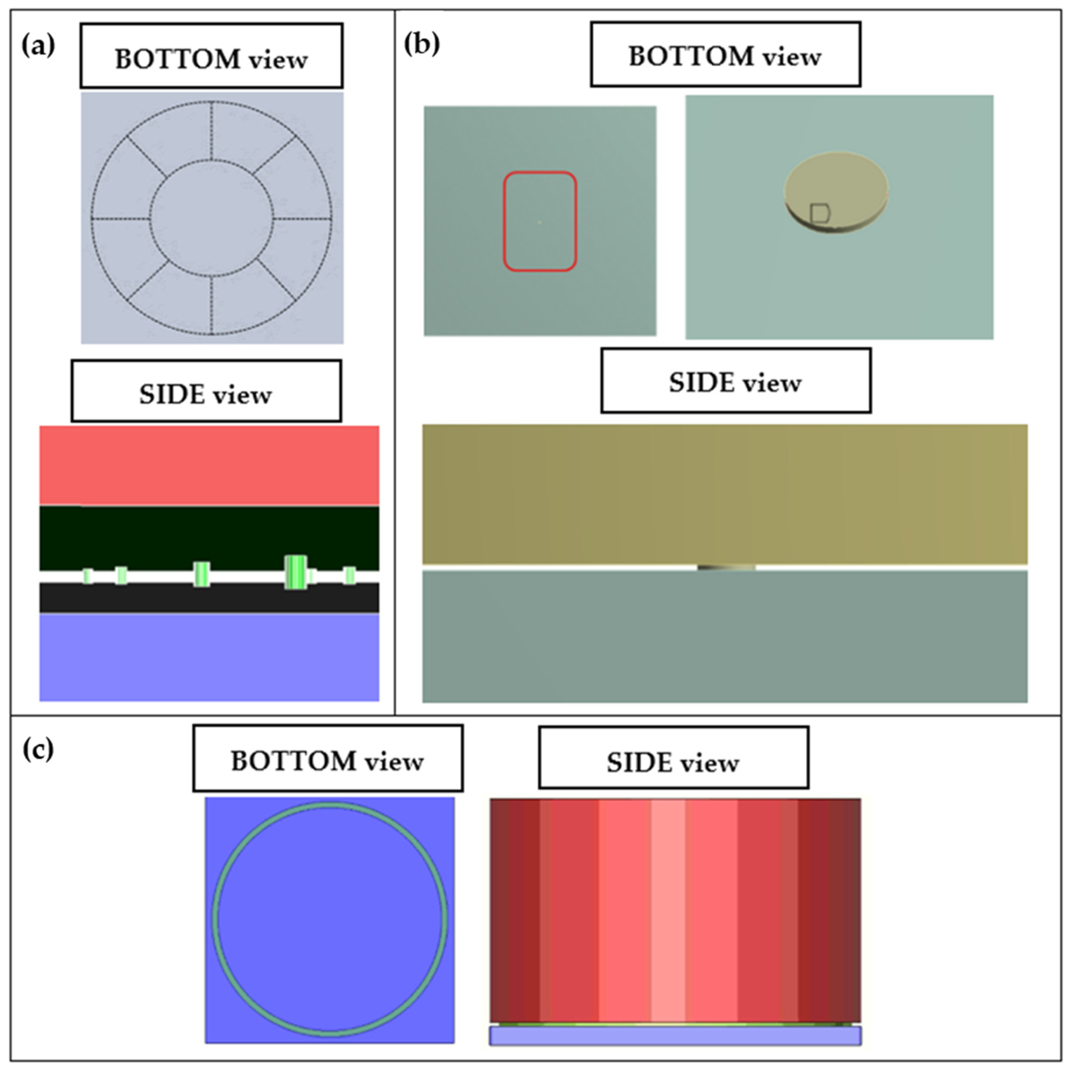
2.3. Geometry and Mesh Layout

The original 3D CAD design of the TIPV converter, including the copper plate heat spreader and the DMS, along with its active cooling system containing water as a coolant with a mean temperature of Tc = 5 °C and a mass flow rate of mc = 0.05 kg/s, is depicted in Figure 3a. In order to save computational costs, since the construction of the domain near the microspacers requires a high amount of cells, a simplified geometry is studied comprising only the cathode, the microspacers and the PV anode, as seen in Figure 3b. At the rear side of the anode close to the cooling system, an appropriate boundary condition is considered to take into account the heat collection by means of the cooling system. Such a simplification of the geometry is mainly implemented because the purpose of this analysis is to test the effect of the different DMS patterns on the total anode temperature, whereas simulation of the cooling system and optimization of its design were already completed in [8].
The different solid components of the system were designed in the CFD model as different solid cell zones with their own thermal properties. Such an approximation was followed as well in [8]. The main properties of the different solid parts (b: thickness, k: thermal conductivity and ε: emissivity) are presented in Table 2.
A 3D conformal grid consisting of tetrahedral elements was constructed in ANSYS Meshing component v17.1 for Cases 1–4. For Cases 5–10, hexahedral elements were used. The construction of such a mesh is challenging due to the presence of elements of different volumes, varying from large-scale (anode, cathode) to micro-scale (DMS). Special attention was paid near the area of the microspacers (a conformal mesh was used to ensure the accuracy and efficiency of the calculations). Because the number of microspacers was variable for the different patterns tested, the number of grid elements varied slightly accordingly, as seen in Table 3. This variable number of cells also affects the computational time per case to reach convergence. However, since steady-state calculations are performed, the needed computational time to reach convergence for each case (by using six parallel cores) does not exceed one hour of real time.
The 3D domain for both the ring shaped DMS patterns and the cumulative area pattern are depicted in Figure 4 (a: Cases 1–4, b: Cases 5–9, c: Case 10).

2.4. Boundary and Initial Conditions

The set of boundary conditions for the solution of the CFD model are presented in Table 4.
The heat flowing from the cathode to the anode Qout is considered equal to the heat reaching the anode. Additionally, at the anode rear side, a steady temperature is assumed considering the presence of the cooling system.

3. Results and Discussion

3.1. Model A (Conduction)

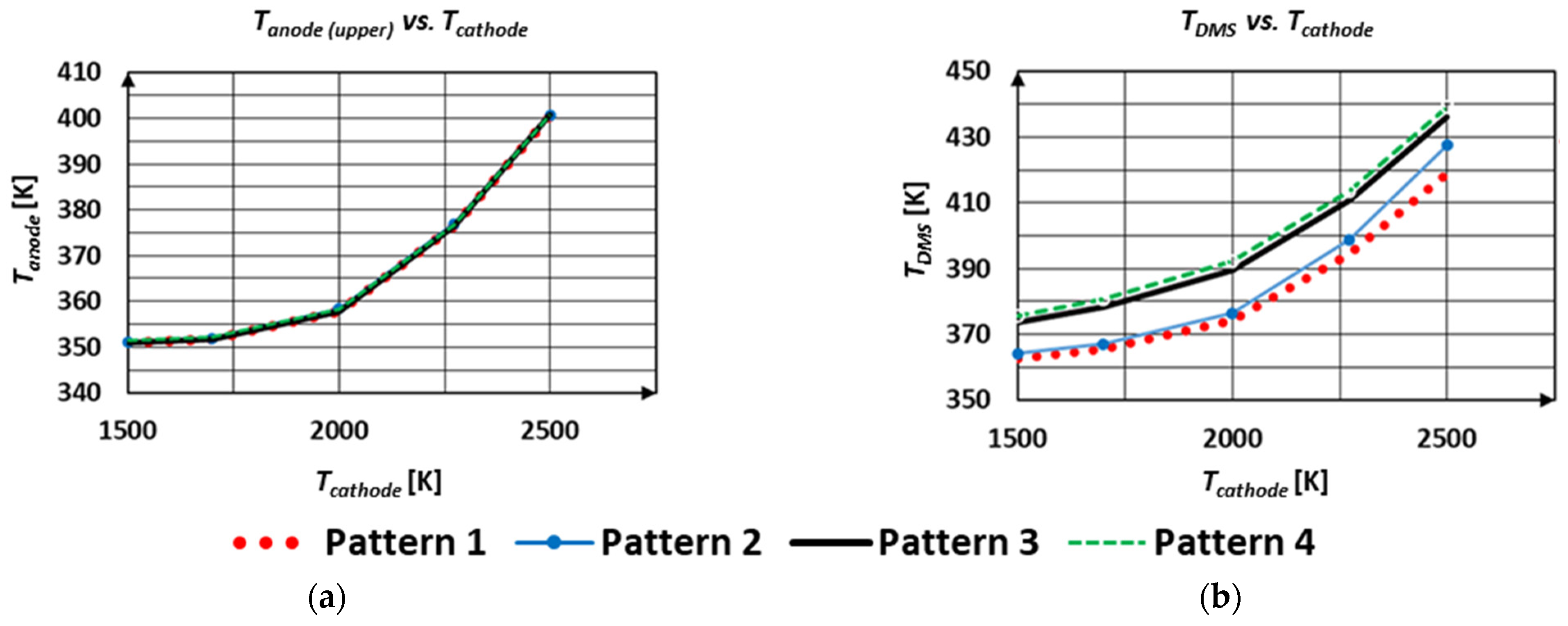
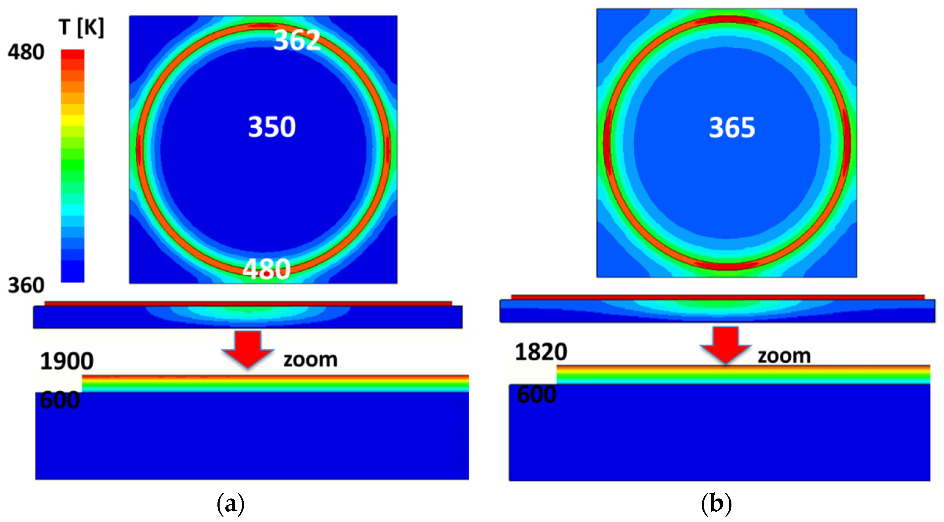
3.1.1. Initial Set of Cases (Patterns 1–4)

Figure 5 presents results of the area-weighted average temperature under different cathode temperatures for patterns 1–4. The areas used to extract results are the anode upper part and the DMS lower part (DMS/anode interface). It can be seen that the anode temperature increases by increasing the cathode temperature for all patterns tested. The worst case in terms of expected anode temperature, both near the microspacers and the anode upper part, is Pattern 4. However, such a temperature increase is not so important, only 1 degree higher than the rest of the patterns tested, as seen in Figure 5a. On the other hand, by increasing the cathode temperature, the DMS temperature increases considerably, especially near the anode section, which can reach a value higher than 380 K for cathode temperatures above 2000 K, as seen in Figure 5b. Nonetheless, even if the microspacers lower temperature increases, the DMS effect on the average anode temperature is not so important since they cover a small fraction (less than 1%) of the total anode surface. Such an observation enhances the results of the 2D model presented in [5].
Figure 6 depicts the spatial distribution of temperature near the microspacers area for a cathode temperature equal to 2273 K for Patterns 1–4. It can be seen that high temperature gradients are induced along the microspacers’ height, a fact that might cause their mechanical failure. Another aspect that needs attention is the presence of thermal hot spots at the anode upper part due to the presence of microspacers. This in turn might lead to small cracking and progressive degradation of the PV cell. Overall, in terms of the thermal point of view, the current microspacers with the specific design and thermal properties act as insulators, and they will not considerably affect the average anode temperature. The only doubts arise in terms of their mechanical stability, especially in a long-term operation of the TIPV converter.

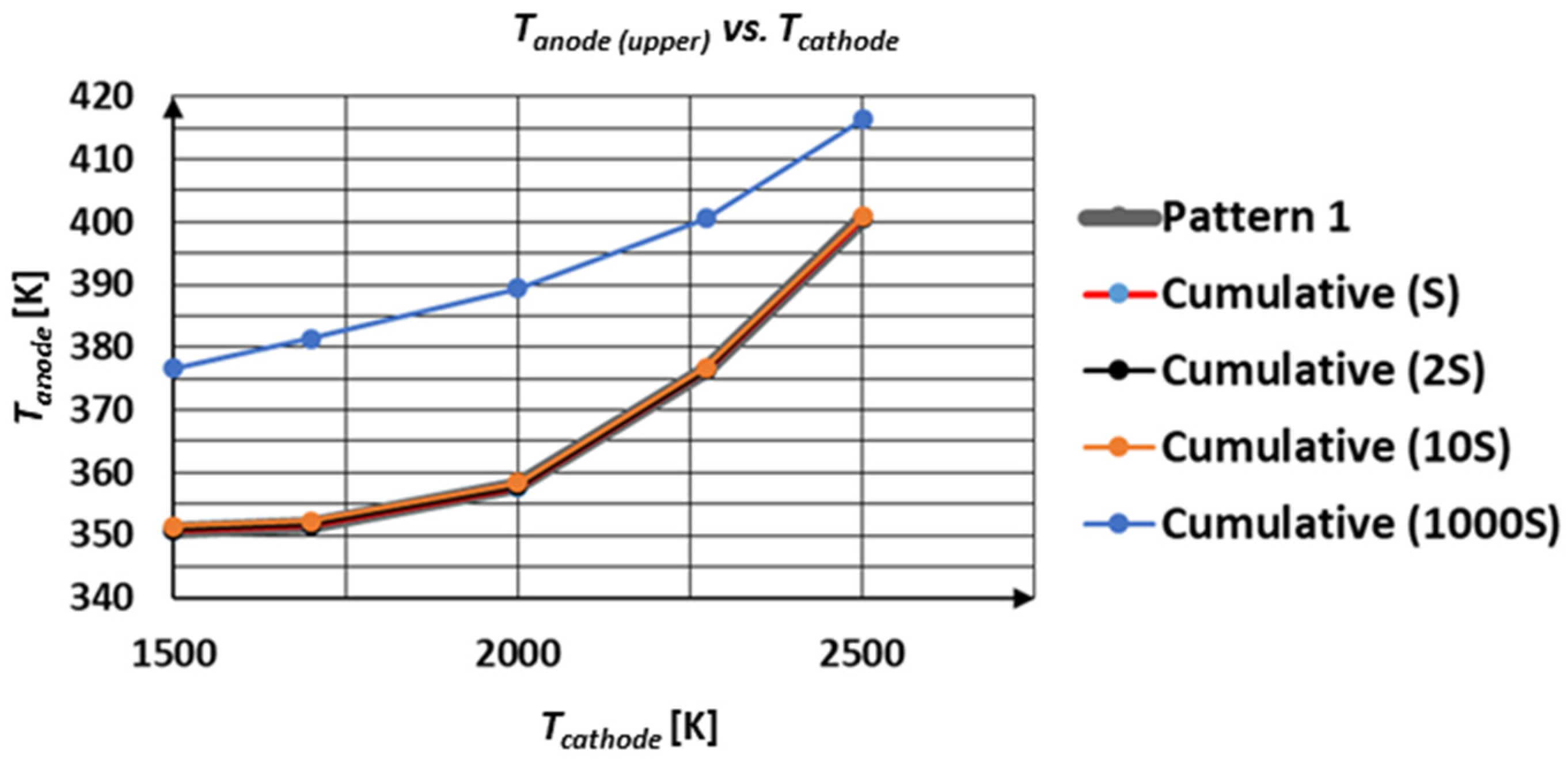
3.1.2. Parametric Study on Different Designs (Cumulative vs. Ring Shape Pattern)

Figure 7 gives a comparison of the area weighted average temperature of the anode upper part between the ring shape and cumulative surface area arrangements. Practically, Pattern 1 and the cumulative arrangement with the same surface coverage have virtually the same results with regard to the average anode temperature. The highest effect in the anode temperature occurs when the anode surface coverage from the microspacers is equal or higher than 5% (Pattern 9—Cumulative S’ = 1000 S).

3.1.3. Sensitivity Analysis on Material Properties

Based on the sensitivity analysis on the microspacer height and thermal conductivity effect on the anode temperature, it was observed that for a microspacer height equal to 1 µm and a thermal conductivity higher than 20 W/(m·K), the anode temperature can increase by almost 10 degrees compared to the reference case (HDMS = 8 µm, kDMS = 1.7 W/(m·K)), as seen in Figure 8. However, even in this case, the total temperature increase is less than 5% of the temperature set near the cooled lower boundary of the anode. This analysis proves once more that even in extreme cases where the microspacers have high thermal conductivity and low height the overall anode temperature is not influenced due to the low surface coverage of the patterns proposed (Patterns 1–4). However, the effect on the local temperature values should be considered in the long-term operation of the TIPV converter.

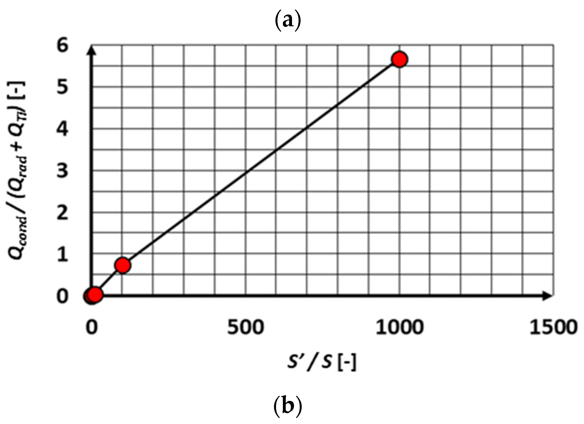
3.2. Model B (Inclusion of Radiation/Thermionic Emission)

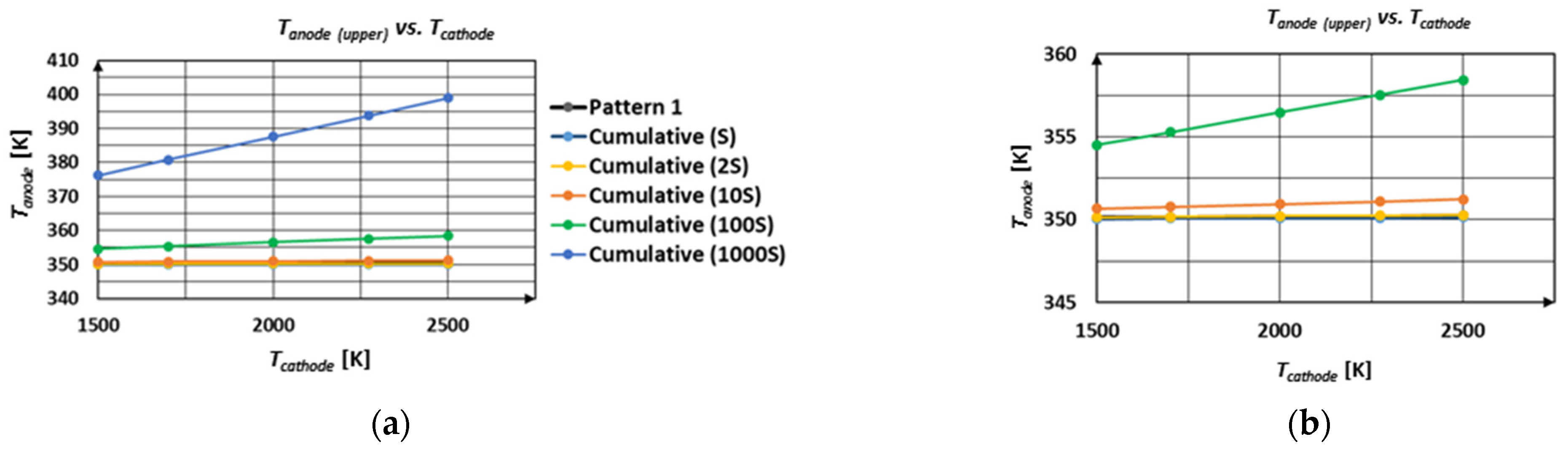
3.2.1. Patterns 1–4 (Ring Shape)

By applying Model B, which takes into account the radiation and thermionic emission between anode/cathode, it can be seen that Patterns 1–4 exhibit a quite similar thermal behavior with regard to the anode’s upper part temperature, thus, almost converging in terms of temperature results (Figure 9a). Some small differences are traced near the DMS/anode interface, with the worst cases being Patterns 3 and 4 due to their higher DMS diameter compared to Patterns 1 and 2 (Figure 9b).
Such observations are reasonable, since in the real application, the main heat transfer, between anode/cathode occurs through radiation and thermionic emission, as seen in Figure 10, especially when the cathode temperature is above 2000 K. The microspacers could affect the anode temperature even more; however, the relevant behavior is not predicted for the proposed 1–4 patterns.

3.2.2. Cumulative Surface Coverage

Figure 11 provides a comparison of the area-weighted average temperature of the anode upper part between the ring shape and cumulative surface area arrangements. Once more, it is proven that Pattern 1 and the cumulative arrangement with the same surface coverage have virtually the same results with regard to the anode temperature. The highest effect in the anode temperature occurs when the anode surface coverage from the microspacers is equal to or higher than 5% (Pattern 9—Cumulative 1000 S). This is attributed to the fact that as the surface coverage increases, the ratio of heat conduction to radiative/thermionic flux increases, as seen in Figure 12. This ratio is more important for lower temperatures, i.e., <2000 K and is not so important when moving to ultra-high temperatures, where the radiative heat flux and the flux due to thermionic emission are considerably high.

3.2.3. Mitigation Risk

Based on the CFD analysis, the commercial ring seems to be a possible alternative to the patterns proposed in this paper in terms of thermal behavior. Such a DMS shape induces a slightly higher anode temperature than patterns 1–4, a fact that is observed both with Model A and B, as seen in Figure 13a. Such a difference is more evident at lower temperatures (<2000 K), since for such operating temperatures, the heat flux due to conduction in the microspacers is more important than the one coming from the cathode to anode, due to thermionic emission and thermal radiation, as seen in Figure 13b.
Some hot spots are also traced near the anode boundaries, as seen in Figure 14, due to the presence of the ring, which might lead to small cracks in the PV anode. An alternative ring with a smaller diameter (higher distance from the anode boundaries) could be a solution for a greater dissipation of the heat flux coming from the cathode due to conduction.

4. Conclusions

A detailed three-dimensional (3D) computational fluid dynamics (CFD) model describing the heat transfer process occurring within a novel cathode-DMS-PV anode-cooling system for hybrid TIPV converters was utilized. A basic system—comprising only the Cathode-DMS-PV anode—was simulated under different operating conditions and various DMS patterns. Both a simplified and a more advanced model were implemented. The first one simulated only the heat transfer through conduction between the different materials, while the second one also took into account the net photon and electron flux between the anode and the cathode. Numerical results indicate that Patterns 1–4—Ring shape arrangement do not significantly influence the mean anode temperature due to the low anode surface (<5%) that they cover. By increasing the anode surface coverage by the DMS, the anode temperature increases accordingly. In any case, in terms of the thermal behavior, the system is not influenced significantly by the DMS Patterns 1–4, even for thermal conductivities up to 80 W/(m·K). In terms of mechanical behavior, a mechanical failure of the microspacers for such patterns is possible due to high temperature gradients between their upper and lower surface, especially for Tcathode > 2000 K. A commercial ring option of capillary shape and height an order of magnitude higher than the proposed patterns seems to be a possible alternative, with lower temperature gradients between its upper and lower part. However, such an option induces a slightly higher anode temperature than patterns 1–4, as well, it could decrease the conversion efficiency due to the large gap. Some hot spots are also traced near the anode boundaries due to the presence of the ring, which might lead to cracks in the PV anode.

Author Contributions

M.Z.: conceptualization, methodology, investigation, writing—original draft preparation, A.B.: conceptualization, investigation, writing—review and editing, G.S.: conceptualization, investigation, writing—review and editing, M.F.: data curation, writing—original draft preparation, V.A.: data curation, writing—original draft preparation, P.S.: data curation, writing—original draft preparation, D.M.T.: supervision, writing—review and editing, funding acquisition, A.N.: supervision, writing—review and editing, D.R.: supervision, writing—review and editing, funding acquisition. All authors have read and agreed to the published version of the manuscript.

Funding

This research has received funding from the European Union’s Horizon 2020 research and innovation programme, AMADEUS (Next GenerAtion MateriAls and Solid State DevicEs for Ultra High Temperature Energy Storage and Conversion), under grant agreement No 737054, https://cordis.europa.eu/project/id/737054.

Institutional Review Board Statement

Not applicable.

Informed Consent Statement

Not applicable.

Data Availability Statement

Not applicable.

Conflicts of Interest

The authors declare no conflict of interest.

Nomenclature

Variables and Parameters
bThicknessSDMSSurface of the DMS
JCThermionic current densityTTemperature
kThermal conductivityεMaterial emissivity
QcondHeat transfer through conductionηTIPVOverall TIPV anode efficiency
Qin-anodeThermal flux heating the anodeΦCMaterial work function
QradNet photon flux emitted from the cathode to the anodeConstants
QradNet photon flux emitted from the anode back to the cathodeAR*Richardson constant value
QTINet electron flux emitted from the cathode to the anodeeElectric charge
QTINet electron flux emitted from the anode back to the cathodekBBoltzmann constant
SanodeSurface of the anodeσStefan–Boltzmann constant

References

  1. Schwede, J.W.; Bargatin, I.; Riley, D.C.; Hardin, B.E.; Rosenthal, S.J.; Sun, Y.; Schmitt, F.; Pianetta, P.; Howe, R.T.; Shen, Z.-X.; et al. Photon-Enhanced Thermionic Emission for Solar Concentrator Systems. Nat. Mater. 2010, 9, 762–767. [Google Scholar] [CrossRef] [PubMed]
  2. Nikolaev, A.L.; Kazmina, M.A.; Lyanguzov, N.V.; Abdulvakhidov, K.G.; Kaidashev, E.M. Synthesis of ZnO Nanorods for Piezoelectric Resonators and Sensors. J. Adv. Dielect. 2022, 12, 2160020. [Google Scholar] [CrossRef]
  3. Manan, A.; Rehman, M.U.; Ullah, A.; Ahmad, A.S.; Iqbal, Y.; Qazi, I.; Khan, M.A.; Shah, H.U.; Wazir, A.H. High Energy Storage Density with Ultra-High Efficiency and Fast Charging–Discharging Capability of Sodium Bismuth Niobate Lead-Free Ceramics. J. Adv. Dielect. 2021, 11, 2150018. [Google Scholar] [CrossRef]
  4. Molokov, A.; Sysoeva, A.; Naberezhnov, A.; Kumar, R.; Koroleva, E.; Vakhrushev, S. Effect of Interface Carbonization on Dielectric Properties of Potassium Nitrate Nanocomposite Based on Porous Glasses. J. Adv. Dielect. 2022, 12, 2250013. [Google Scholar] [CrossRef]
  5. Bellucci, A.; Sabbatella, G.; Girolami, M.; Mastellone, M.; Serpente, V.; Mezzi, A.; Kaciulis, S.; Paci, B.; Generosi, A.; Polini, R.; et al. Dielectric Micro- and Sub-Micrometric Spacers for High-Temperature Energy Converters. Energy Technol. 2021, 9, 2000788. [Google Scholar] [CrossRef]
  6. Dielectric MicroSpacer Technology. Available online: https://cordis.europa.eu/project/id/754568 (accessed on 22 December 2022).
  7. Stamatopoulos, P.; Zeneli, M.; Nikolopoulos, A.; Bellucci, A.; Trucchi, D.M.; Nikolopoulos, N. Introducing a 1D Numerical Model for the Simulation of PN Junctions of Varying Spectral Material Properties and Operating Conditions. Energy Convers. Manag. 2021, 230, 113819. [Google Scholar] [CrossRef]
  8. Zeneli, M.; Bellucci, A.; Sabbatella, G.; Trucchi, D.M.; Nikolopoulos, A.; Nikolopoulos, N.; Karellas, S.; Kakaras, E. Performance Evaluation and Optimization of the Cooling System of a Hybrid Thermionic-Photovoltaic Converter. Energy Convers. Manag. 2020, 210, 112717. [Google Scholar] [CrossRef]
  9. Bellucci, A.; Linares, P.G.; Villa, J.; Martí, A.; Datas, A.; Trucchi, D.M. Hybrid Thermionic-Photovoltaic Converter with an In0.53Ga0.47As Anode. Sol. Energy Mater. Sol. Cells 2022, 238, 111588. [Google Scholar] [CrossRef]
  10. Bellucci, A.; García-Linares, P.; Martí, A.; Trucchi, D.M.; Datas, A. A Three-Terminal Hybrid Thermionic-Photovoltaic Energy Converter. Adv. Energy Mater. 2022, 12, 2200357. [Google Scholar] [CrossRef]
  11. Qiu, H.; Lin, S.; Xu, H.; Hao, G.; Xiao, G. Hybrid Thermionic-Photovoltaic Converter with Graphene-on-Semiconductor Heterojunction Anode for Efficient Electricity Generation. Iscience 2022, 25, 105051. [Google Scholar] [CrossRef] [PubMed]
  12. Campbell, M.F.; Celenza, T.J.; Schmitt, F.; Schwede, J.W.; Bargatin, I. Progress Toward High Power Output in Thermionic Energy Converters. Adv. Sci. 2021, 8, 2003812. [Google Scholar] [CrossRef] [PubMed]
  13. Campbell, M.F.; Azadi, M.; Lu, Z.; Eskenazi, A.G.; Jain, A.; Bang, J.W.; Sieg, P.G.; Popov, G.A.; Nicaise, S.M.; Van Houten, K.C.; et al. Nanostructured Spacers for Thermionic and Thermophotovoltaic Energy Converters. J. Microelectromech. Syst. 2020, 29, 637–644. [Google Scholar] [CrossRef]
  14. Wang, H.; Loveless, A.M.; Darr, A.M.; Garner, A.L. Experimental Studies of Gas Breakdown and Electron Emission for Nanoscale Vacuum Gaps. In Proceedings of the 2022 IEEE International Conference on Plasma Science (ICOPS), Seattle, WA, USA, 22–26 May 2022; pp. 1–2. [Google Scholar] [CrossRef]
  15. Nicaise, S.M.; Lin, C.; Azadi, M.; Bozorg-Grayeli, T.; Adebayo-Ige, P.; Lilley, D.E.; Pfitzer, Y.; Cha, W.; Van Houten, K.; Melosh, N.A.; et al. Micron-Gap Spacers with Ultrahigh Thermal Resistance and Mechanical Robustness for Direct Energy Conversion. Microsyst. Nanoeng. 2019, 5, 31. [Google Scholar] [CrossRef] [PubMed] [Green Version]
  16. Lee, J.-H.; Bargatin, I.; Melosh, N.A.; Howe, R.T. Optimal Emitter-Collector Gap for Thermionic Energy Converters. Appl. Phys. Lett. 2012, 100, 173904. [Google Scholar] [CrossRef] [Green Version]
  17. Rahman, E.; Nojeh, A. Interplay between Near-Field Radiative Coupling and Space-Charge Effects in a Microgap Thermionic Energy Converter under Fixed Heat Input. Phys. Rev. Appl. 2020, 14, 024082. [Google Scholar] [CrossRef]
  18. Jensen, D.; Taufiq Elahi, A.N.M.; Ghashami, M.; Park, K. Submicrometer-Gap Thermionic Power Generation Based on Comprehensive Modeling of Charge and Thermal Transport. Phys. Rev. Appl. 2021, 15, 024062. [Google Scholar] [CrossRef]
  19. Go, D.B.; Haase, J.R.; George, J.; Mannhart, J.; Wanke, R.; Nojeh, A.; Nemanich, R. Thermionic Energy Conversion in the Twenty-First Century: Advances and Opportunities for Space and Terrestrial Applications. Front. Mech. Eng. 2017, 3, 13. [Google Scholar] [CrossRef] [Green Version]
  20. CORDIS, European Commission Production Method Of Electrical Energy by Enhanced Thermal Electron Emission by the Use of Superior Semiconductors. Available online: https://cordis.europa.eu/project/id/308975/reporting (accessed on 12 December 2022).
  21. Ahmad, T.; Plee, S.L.; Myers, J.P. ANSYS Fluent Theory Guide 2013. Available online: http://www.pmt.usp.br/academic/martoran/notasmodelosgrad/ANSYS%20Fluent%20Theory%20Guide%2015.pdf (accessed on 12 December 2022).
  22. Datas, A. Hybrid Thermionic-Photovoltaic Converter. Appl. Phys. Lett. 2016, 108, 143503. [Google Scholar] [CrossRef] [Green Version]
  23. Datas, A.; Vaillon, R. Thermionic-Enhanced near-Field Thermophotovoltaics. Nano Energy 2019, 61, 10–17. [Google Scholar] [CrossRef]
  24. Li, W.; Peng, W.; Yang, Z.; Su, G.; Su, S.; Chen, J. Performance Improvements and Parametric Design Strategies of an Updated Thermionic-Photovoltaic Converter. Phys. Scr. 2020, 95, 035208. [Google Scholar] [CrossRef]
Figure 1. (a) DMS mask proposed in the shape of rings (b) cumulative area coverage of the DMS, (c) commercial ring (capillary shape).
Sustainability 15 01786 g001
Figure 2. Solution of photon/electron flux interexchange between anode/cathode.
Sustainability 15 01786 g002
Figure 3. TIPV converter/Cooling system (a) initial (detailed) and (b) simplified one.
Sustainability 15 01786 g003aSustainability 15 01786 g003b
Figure 4. 3D discretized domain of the studied system for (a) DMS mask proposed in the shape of ring (b) Cumulative area coverage of the DMS and (c) commercial ring.
Sustainability 15 01786 g004
Figure 5. Area weighted average temperature results under various cathode temperatures for the (a) anode (b) DMS/anode interface (Model A: Patterns 1–4).
Sustainability 15 01786 g005
Figure 6. Contours of the anode upper part temperature for Tcathode = 2273 K, (a) Pattern 1, (b) Pattern 2, (c) Pattern 3, and, (d) Pattern 4.
Sustainability 15 01786 g006aSustainability 15 01786 g006b
Figure 7. Comparison of the anode temperature results for the ring shape (Pattern 1) and cumulative shape arrangement under various cathode temperatures (a) Pattern 1 vs. Cumulative S-1000S (b) Pattern 1 vs. Cumulative S-100S.
Sustainability 15 01786 g007
Figure 8. (a) Area weighted average temperature results under various DMS thermal conductivities and heights for the anode upper part and (b) TDMS,upper − TDMS,bottom/TDMS,upper ratio (Tcathode = 2273 K).
Sustainability 15 01786 g008
Figure 9. Area weighted average temperature results under various cathode temperatures for the (a) anode (b) DMS/anode interface (Model B: Patterns 1–4).
Sustainability 15 01786 g009
Figure 10. Ratio of heat transfer through conduction (Qcond) to the sum of the heat transfer through radiation and thermionic emission (Qrad + QTI) under various cathode temperatures.
Sustainability 15 01786 g010
Figure 11. Area-weighted average temperature results under various cathode temperatures of the anode upper part.
Sustainability 15 01786 g011
Figure 12. Ratio of heat transfer through conduction (Qcond) to the sum of the heat transfer through radiation and thermionic emission (Qrad + QTI) (a) under various cathode temperatures (b) vs. DMS surface coverage (S’: DMS surface, S: Surface coverage of reference case—Pattern 1).
Sustainability 15 01786 g012aSustainability 15 01786 g012b
Figure 13. (a) Area-weighted average temperature results of the anode upper part and (b) ratio of heat transfer through conduction (Qcond) to the sum of the heat transfer through radiation and thermionic emission (Qrad + QTI) under various cathode temperatures.
Sustainability 15 01786 g013
Figure 14. Temperature contours of the anode upper part for (a) Model A and (b) Model B.
Sustainability 15 01786 g014
Table 1. DMS patterns tested.
Pattern NumberShapeDMS Height (μm)DMS Diameter (μm)Number of DMSSDMS (mm2)SDMS/Sanode (mm2/mm2)
1Ring852615.12 × 10−35.12 × 10⁻⁵
2Ring856631.25 × 10−21.25 × 10⁻⁴
3Ring8101269.89 × 10−39.89 × 10⁻⁵
4Ring8103232.45 × 10−22.45 × 10⁻⁴
5Cumulative880.715.12 × 10−35.12 × 10⁻⁵
6Cumulative811411.02 x 10−21.02 x 10⁻⁴
7Cumulative825515.12 × 10−25.12 × 10⁻⁴
8Cumulative880715.12 × 10−15.12 × 10⁻³
9Cumulative8255315.125.12 × 10−2 (5.12%)
10Commercial1009500 (Out)/
9000 (In)
17.2657.3 × 10−2 (7.26%)
Table 2. PV anode, DMS and cathode thermal properties.
Componentb (mm)k (W/(m·K))ε (-)
Cathode (W)61000.28
DMS (ZrO2)8 × 10−3 *1.7 **-
Anode (GaAs)0.5460.6
* In most of the cases, it is equal to 8 μm, but a parametric study was also conducted on the DMS height. ** In most of the cases, it is equal to 1.7 W/(m·K), but a parametric study was also conducted.
Table 3. Number of elements used for the different studied patterns.
Pattern Number12345–910
Number of elements [millions]3.34.73.734.060.5–0.60.132
Table 4. Boundary conditions set at the TIPV converter system.
ComponentBC TypeParametersUnitsValues
Cathode lowerWallQoutW/m2*
Cathode upperWallTK1500–2500
Anode lowerWallTK350
Anode upperWallQin-anodeW/m2*
External WallsAdiabatic walls
* either zero in Model A or Qrad + QTI for Model B.
Disclaimer/Publisher’s Note: The statements, opinions and data contained in all publications are solely those of the individual author(s) and contributor(s) and not of MDPI and/or the editor(s). MDPI and/or the editor(s) disclaim responsibility for any injury to people or property resulting from any ideas, methods, instructions or products referred to in the content.

