Article

Modeling of Non-Characteristic Third Harmonics Produced by Voltage Source Converter under Unbalanced Condition

State Grid Shanxi Electric Power Research Institute, Taiyuan 030024, China
*
Author to whom correspondence should be addressed.
Sustainability 2022, 14(11), 6449; https://doi.org/10.3390/su14116449
Submission received: 25 April 2022 / Revised: 17 May 2022 / Accepted: 17 May 2022 / Published: 25 May 2022
(This article belongs to the Topic Zero Carbon Vehicles and Power Generation)

Abstract

:
A three-phase three-wire voltage source converter (VSC) can produce third harmonics when it is operated under an unbalanced condition. It is essential to understand the mechanism of the production of this third harmonic and to assess its impact on power systems. Therefore, this paper presents an analytical model of the VSC under the unbalanced condition through mathematical derivations, and the final model is a coupled Thevenin circuit. The proposed model allows for direct computation of the non-characteristic third harmonics through harmonic power flow studies. The results show that VSC under unbalanced conditions emits both positive-sequence and negative-sequence third harmonics, and that the positive-sequence third harmonic is much larger than the negative-sequence third harmonic. It also shows that the unbalanced level and the size of the dc-link capacitor are critical to the level of non-characteristic third harmonics. The correctness of the proposed model and its application on noncharacteristic third harmonic evaluations have been verified using EMT simulations.

1. Introduction

In this context, this paper presents an analytical model of the VSC under unbalanced conditions for the direct computation of the non-characteristic third harmonics through rigorous mathematical derivations. The new model reveals the mechanism of the generation of third harmonics and the characteristics of third harmonics. The new model shows that a Thevenin circuit can represent the VSC for both the positive-sequence and negative-sequence third harmonics. In addition, there are coupling effects between the positive-sequence and negative-sequence third harmonics. The model also shows that the positive-sequence third harmonic is much larger than the negative-sequence third harmonic. The computation of the source and the impedance of the developed Thevenin model requires positive-sequence and negative-sequence fundamental frequency voltage and current on the ac side of the VSC, which can be obtained through load flow studies.
Power electronic devices have experienced a dramatic increase in modern power systems due to the initiative of renewable energies such as wind power generation and photovoltaic (PV) [1], and other applications such as flexible AC transmission system (FACTS) and high voltage DC (HVDC) transmission [2,3]. In recent years, the voltage source converter (VSC) has become the most popular basis of power electronic devices due to its advantages of bidirectional power flow and independent control of active and reactive power [4]. With the massive integration of these VSC devices, there is a concern about their harmonic impact on power systems [5,6,7]. Under the normal condition, VSC devices only produce very-high-frequency harmonics, which is produced by the PWM switching, but such harmonics can generally be impeded by a passive filter in front of the VSC [8,9]. However, VSC devices can generate low-order non-characteristic third harmonics under the unbalanced condition, which is a power quality concern of power systems. Such a phenomenon occurs because the unbalanced fundamental frequency voltage and current on the ac side of the VSC can induce second harmonic ripples in the dc-link voltage of the VSC through the switching process [9]. These second harmonic ripples in the dc-link voltage, in turn, will lead to a third harmonic voltage on the ac side of the VSC, again through the switching process. As a result, under the unbalanced condition, the VSC becomes a voltage source at the third harmonic. Therefore, it is essential to understand the mechanism of the production of the third harmonic voltage, especially in the distribution system, which can be unbalanced since single-phase loads are dominant [10]. A computation method of the third harmonics under the unbalanced conditions is also needed to assess their impacts.
To date, there are numerous papers presenting the studies of the VSC under unbalanced conditions, but most of these works focus on the control strategies that can suppress the unbalanced condition-induced third harmonics [11,12,13,14]. These papers have shown that the unbalanced fundamental frequency voltage and current will lead to double-frequency power oscillation on the ac side of the VSC. As a result, the dc side experiences second harmonic voltage, which can lead to third harmonics on the ac side of the VSC. Based on this finding, the control schemes that can be used to suppress the second harmonic on the dc-link are designed in [12,13]. However, these papers do not provide an analytical algorithm to compute the second harmonic on the dc side or the third harmonic on the ac side. A few other works are proposed specifically for assessing VSC’s third harmonic emission under unbalanced conditions [15,16,17]. In [15], the switching function of the VSC and the harmonic interaction between the ac side and dc side of the VSC are analyzed to obtain the model that can be used to compute the third harmonic distortion. Nevertheless, the impact of the third harmonic on the switching function is not included in this method. Thus, the result could be inaccurate. In [16], the oscillation between the dc side and ac side of the VSC is analyzed based on the ac/dc power interaction, which reveals the mechanism of the production of the third harmonic, but the final analytical method of the uncharacteristic third harmonics is not presented. The reference [17] further provides a method for assessing the third harmonic distortions using the power interaction between the ac side and dc side of the VSC. However, the proposed model omits the effect of the control loop so that the model is not accurate. Moreover, this method is not able to fully show the differences between the positive-sequence and negative-sequence third harmonics and the coupling effect between these two kinds of third harmonics. References [18,19] propose a method that can be used to reveal the harmonic characteristics of the VSC by analyzing the control and AC/DC interaction, but the non-characteristic third harmonics are not analyzed. In summary, a full model that reveals the characteristics of third harmonics produced by VSC is still desired.
This paper presents an analytical model of the VSC under unbalanced conditions for the direct computation of the non-characteristic third harmonics through rigorous mathematical derivations. The development of the new model reveals the mechanism of the generation of third harmonics and their characteristics. The new model shows that a Thevenin circuit can represent the VSC at both the positive-sequence and negative-sequence third harmonics. In addition, there are coupling effects between the positive-sequence and negative-sequence third harmonics. The model also shows that the positive-sequence third harmonic is much larger than the negative-sequence third harmonic. The computation of the source and the impedance of the developed Thevenin model requires a positive-sequence and negative-sequence fundamental frequency voltage and current on the ac side of the VSC, which can be obtained through load flow studies.
The rest of this paper is organized as follows. Section 2 explains the mechanism of generating the non-characteristic third harmonics by the VSC under unbalanced conditions. Section 3 presents the development of the model of VSC under unbalanced conditions for a non-characteristic third harmonic. The proposed model is validated via time-domain simulations in Section 4. Section 5 shows some discussions on the proposed model.

2. Mechanism of the Production of Noncharacteristic Third Harmonics

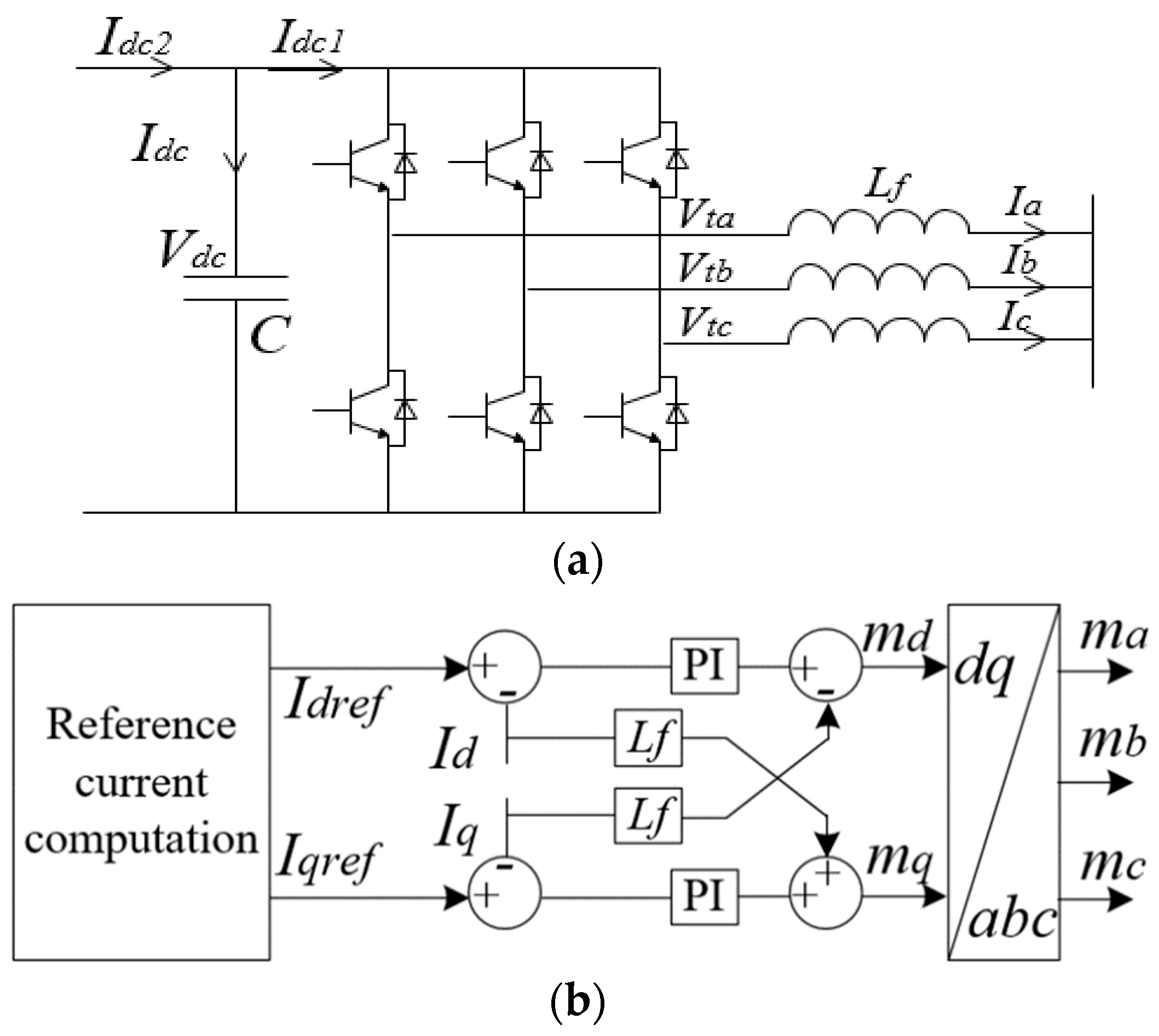
A typical VSC system is illustrated in Figure 1a, and the control strategy of this VSC is presented in Figure 1b. As one can see, a two-loop control scheme is used, and the outer control loop is used to generate the reference current for the inner current control. The current is controlled using a PI regulator. A capacitor contains the dc-link voltage of the VSC. An inductor Lf is connected at the front end of the VSC to filter out the switching harmonics.
Under the unbalanced operational condition, there are positive-sequence and negative-sequence fundamental frequency voltage and current on the AC side of the VSC, and the three-phase current can be expressed as
I a ( t ) = I 1 + cos ( ω 1 t + δ 1 + ) + I 1 cos ( ω 1 t + δ 1 ) I b ( t ) = I 1 + cos ( ω 1 t + δ 1 + 120 ° ) + I 1 cos ( ω 1 t + δ 1 + 120 ° ) I c ( t ) = I 1 + cos ( ω 1 t + δ 1 + + 120 ° ) + I 1 cos ( ω 1 t + δ 1 120 ° )
It is noted that the modulation signal is a result of the inner current control, so the modulation signal contains the same types of components as those in the current. Thus, the three-phase modulation signals can be expressed as
m a ( t ) = m 1 + cos ( ω 1 t + θ 1 + ) + m 1 cos ( ω 1 t + θ 1 ) m b ( t ) = m 1 + cos ( ω 1 t + θ 1 + 120 ° ) + m 1 cos ( ω 1 t + θ 1 + 120 ° ) m c ( t ) = m 1 + cos ( ω 1 t + θ 1 + + 120 ° ) + m 1 cos ( ω 1 t + θ 1 120 ° )
Since we focus on the study of the third harmonic, the high-frequency harmonics in the switching function can be omitted. Consequently, the modulation signal can be used to represent the switching function of the VSC. As a result, based on (1) and (2), the current on the DC side can be computed as
I d c ( t ) = m a ( t ) I a ( t ) + m b ( t ) I b ( t ) + m c ( t ) I c ( t ) = 3 2 m 1 + I 1 + cos ( θ 1 + δ 1 + ) + 3 2 m 1 I 1 cos ( θ 1 δ 1 ) + 3 2 m 1 + I 1 cos ( 2 ω 1 t + θ 1 + + δ 1 ) + 3 2 m 1 I 1 + cos ( 2 ω 1 t + θ 1 + δ 1 + )
According to the above DC side current, the voltage on the DC-link capacitor can be written as
V d c ( t ) = 1 C 0 t i d c ( t ) d t + V d c ( 0 ) = V d c 0 + 3 4 C ω 1 m 1 + I 1 cos ( 2 ω 1 t + θ 1 + + δ 1 π 2 ) + 3 4 C ω 1 m 1 I 1 + cos ( 2 ω 1 t + θ 1 + δ 1 + π 2 )
where Vdc0 is the steady-state dc-link voltage. It can be seen that, due to the unbalanced condition, there are second harmonic ripples in the dc-link voltage. It is noteworthy that the expression in (4) is obtained on the basis that all dc-side harmonic currents pass through the dc-link capacitor. In practice, there will be a load (or source) on the other side of the dc-link that has an equivalent impedance Zload, and the harmonic components in Idc will be distributed between the load and dc-link capacitor (Idc1 and Idc2 in Figure 1a), that is, all of the harmonic components in (4) will be multiplied by Zload/(Zload + ZC). For simplification but not losing generality, Zload is assumed to be very large so it can be ignored. The DC-link voltage in (4) is converted to AC voltage through the switching process, obtaining the expressions of the three-phase voltages, which are expressed in (5)~(7).
As one can see from (5)~(7), there are third harmonic components in the three-phase voltage of the VSC. In addition, it is found that the third harmonic voltages contain both positive-sequence or negative-sequence components, which are different from the conventional zero-sequence third harmonic. It can also be noted that the third harmonic is in the form of a voltage that is only affected by the positive-sequence and negative-sequence fundamental frequency components.
V t a ( t ) = m a ( t ) V d c ( t ) = { m 1 + cos ( ω 1 t + θ 1 + ) + m 1 cos ( ω 1 t + θ 1 ) } V d c 0 + 3 8 ω 1 C m 1 + 2 I 1 cos ( ω 1 t + δ 1 π 2 ) + 3 8 ω 1 C m 1 + m 1 I 1 cos ( ω 1 t + θ 1 + θ 1 + δ 1 π 2 ) + 3 8 ω 1 C m 1 m 1 + I 1 + cos ( ω 1 t + θ 1 θ 1 + + δ 1 + π 2 ) + 3 8 ω 1 C m 1 2 I 1 + cos ( ω 1 t + δ 1 + π 2 ) + 3 8 ω 1 C m 1 + 2 I 1 cos ( 3 ω 1 t + 2 θ 1 + + δ 1 π 2 ) + 3 8 ω 1 C m 1 + m 1 I 1 cos ( 3 ω 1 t + θ 1 + + θ 1 + δ 1 π 2 ) + 3 8 ω 1 C m 1 m 1 + I 1 + cos ( 3 ω 1 t + θ 1 + θ 1 + + δ 1 + π 2 ) + 3 8 ω 1 C m 1 2 I 1 + cos ( 3 ω 1 t + 2 θ 1 + δ 1 + π 2 )
V t b ( t ) = m b ( t ) V d c ( t ) = { m 1 + cos ( ω 1 t + θ 1 + 120 ° ) + m 1 cos ( ω 1 t + θ 1 + 120 ° ) } V d c 0 + 3 8 ω 1 C m 1 + 2 I 1 cos ( 3 ω 1 t + 2 θ 1 + + δ 1 π 2 120 ° ) + 3 8 ω 1 C m 1 + 2 I 1 cos ( ω 1 t + δ 1 π 2 + 120 ° ) + 3 8 ω 1 C m 1 + m 1 I 1 cos ( 3 ω 1 t + θ 1 + + θ 1 + δ 1 π 2 + 120 ° ) + 3 m 8 ω 1 C m 1 + m 1 I 1 cos ( ω 1 t + θ 1 + θ 1 + δ 1 π 2 120 ° ) + 3 8 ω 1 C m 1 m 1 + I 1 + cos ( 3 ω 1 t + θ 1 + θ 1 + + δ 1 + π 2 120 ° ) + 3 8 ω 1 C m 1 m 1 + I 1 + cos ( ω 1 t + θ 1 θ 1 + + δ 1 + π 2 + 120 ° ) + 3 8 ω 1 C m 1 2 I 1 + cos ( 3 ω 1 t + 2 θ 1 + δ 1 + π 2 + 120 ° ) + 3 8 ω 1 C m 1 2 I 1 + cos ( ω 1 t + δ 1 + π 2 120 ° )
V t c ( t ) = m c ( t ) V d c ( t ) = { m 1 + cos ( ω 1 t + θ 1 + 120 ° ) + m 1 cos ( ω 1 t + θ 1 + 120 ° ) } V d c 0 + 3 8 ω 1 C m 1 + 2 I 1 cos ( 3 ω 1 t + 2 θ 1 + + δ 1 π 2 + 120 ° ) + 3 8 ω 1 C m 1 + 2 I 1 cos ( ω 1 t + δ 1 π 2 120 ° ) + 3 8 ω 1 C m 1 + m 1 I 1 cos ( 3 ω 1 t + θ 1 + + θ 1 + δ 1 π 2 120 ° ) + 3 8 ω 1 C m 1 + m 1 I 1 cos ( ω 1 t + θ 1 + θ 1 + δ 1 π 2 + 120 ° ) + 3 8 ω 1 C m 1 m 1 + I 1 + cos ( 3 ω 1 t + θ 1 + θ 1 + + δ 1 + π 2 + 120 ° ) + 3 8 ω 1 C m 1 m 1 + I 1 + cos ( ω 1 t + θ 1 θ 1 + + δ 1 + π 2 120 ° ) + 3 8 ω 1 C m 1 2 I 1 + cos ( 3 ω 1 t + 2 θ 1 + δ 1 + π 2 120 ° ) + 3 8 ω 1 C m 1 2 I 1 + cos ( ω 1 t + δ 1 + π 2 + 120 ° )

3. Modeling VSC under Unbalanced Condition

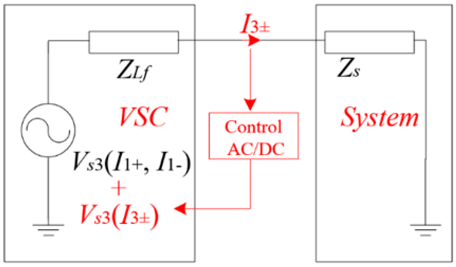
The above analysis has shown that an unbalanced condition can introduce a third harmonic voltage for the VSC. Such a third harmonic voltage will further introduce a third harmonic current in the interconnected grid. As a result of the current feedback control strategy, the third harmonic current would lead to an additional third harmonic voltage on the ac side of the VSC via the control section. As a result, the third harmonic voltage of the VSC shall be computed as shown in Figure 2. As can be seen, there are two parts to be included. The first is the third harmonic voltage caused by the fundamental frequency voltage and current, and the second is the distribution of this third harmonic voltage. To compute the final voltage, it is necessary to include the third harmonic on the ac side of the VSC, and, as a result, the steady-state current and modulation signal can be expressed as (8) and (9).
Figure 2. Illustration of modeling of the third harmonic.
Sustainability 14 06449 g002
I a ( t ) = I 1 + cos ( ω 1 t + δ 1 + ) + I 1 cos ( ω 1 t + δ 1 ) + I 3 + cos ( 3 ω 1 t + δ 3 + ) + I 3 cos ( 3 ω 1 t + δ 3 ) I b ( t ) = I 1 + cos ( ω 1 t + δ 1 + 120 ° ) + I 1 cos ( ω 1 t + δ 1 + 120 ° ) + I 3 + cos ( 3 ω 1 t + δ 3 + 120 ° ) + I 3 cos ( 3 ω 1 t + δ 3 + 120 ° ) I c ( t ) = I 1 + cos ( ω 1 t + δ 1 + + 120 ° ) + I 1 cos ( ω 1 t + δ 1 120 ° ) + I 3 + cos ( 3 ω 1 t + δ 3 + + 120 ° ) + I 3 cos ( 3 ω 1 t + δ 3 120 ° )
m a = m 1 + cos ( ω 1 t + θ 1 + ) + m 1 cos ( ω 1 t + θ 1 )   + m 3 + cos ( 3 ω 1 t + θ 3 + ) + m 3 cos ( 3 ω 1 t + θ 3 ) m b = m 1 + cos ( ω 1 t + θ 1 + 120 ° ) + m 1 cos ( ω 1 t + θ 1 + 120 ° )   + m 3 + cos ( 3 ω 1 t + θ 3 + 120 ° ) + m 3 cos ( 3 ω 1 t + θ 3 + 120 ° ) m c = m 1 cos ( ω 1 t + θ 1 + + 120 ° ) + m 1 cos ( ω 1 t + θ 1 120 ° )   + m 3 + cos ( 3 ω 1 t + θ 3 + + 120 ° ) + m 3 cos ( 3 ω 1 t + θ 3 120 ° )
The equations in (8) and (9) can be used to obtain the current on the DC side, which is given as (10):
I d c ( t ) = m a ( t ) I a ( t ) + m b ( t ) I b ( t ) + m c ( t ) I c ( t ) = 3 2 { m 1 + I 1 + cos ( θ 1 + δ 1 + ) + m 1 + I 1 cos ( 2 ω 1 t + θ 1 + + δ 1 ) + m 1 + I 3 + cos ( 2 ω 1 t + δ 3 + θ 1 + ) + m 1 + I 3 cos ( 4 ω 1 t + δ 3 + θ 1 + ) + m 1 I 1 + cos ( 2 ω 1 t + θ 1 + δ 1 + ) + m 1 I 1 cos ( θ 1 δ 1 ) + m 1 I 3 + cos ( 4 ω 1 t + δ 3 + + θ 1 ) + m 1 I 3 cos ( 2 ω 1 t + δ 3 θ 1 ) + m 3 + I 1 + cos ( 2 ω 1 t + θ 3 + δ 1 + ) + m 3 + I 1 cos ( 4 ω 1 t + θ 3 + + δ 1 ) + m 3 + I 3 + cos ( θ 3 + δ 3 + ) + m 3 + I 3 cos ( 6 ω 1 t + θ 3 + + δ 3 ) + m 3 I 1 + cos ( 4 ω 1 t + θ 3 + δ 1 + ) + m 3 I 1 cos ( 2 ω 1 t + θ 3 δ 1 ) + m 3 I 3 + cos ( 6 ω 1 t + δ 3 + + θ 3 ) + m 3 I 3 2 cos ( θ 3 δ 3 ) }
Accordingly, the DC-link voltage can be computed as
V d c ( t ) = 1 C 0 t i d c d t + V d c 0 = V d c 0 + { 3 4 C ω 1 m 1 + I 1 cos ( 2 ω 1 t + θ 1 + + δ 1 π 2 ) + 3 4 C ω 1 m 1 + I 3 + cos ( 2 ω 1 t + δ 3 + θ 1 + π 2 ) + 3 8 C ω 1 m 1 + I 3 cos ( 4 ω 1 t + δ 3 + θ 1 + π 2 ) + 3 4 C ω 1 m 1 I 1 + cos ( 2 ω 1 t + θ 1 + δ 1 + π 2 ) + 3 8 C ω 1 m 1 I 3 + cos ( 4 ω 1 t + δ 3 + + θ 1 π 2 ) + 3 4 C ω 1 m 1 I 3 cos ( 2 ω 1 t + δ 3 θ 1 π 2 ) + 3 4 C ω 1 m 3 + I 1 + cos ( 2 ω 1 t + θ 3 + δ 1 + π 2 ) + 3 8 C ω 1 m 3 + I 1 cos ( 4 ω 1 t + θ 3 + + δ 1 ) + 3 12 C ω 1 m 3 + I 3 cos ( 6 ω 1 t + θ 3 + + δ 3 ) + 3 8 C ω 1 m 3 I 1 + cos ( 4 ω 1 t + θ 3 + δ 1 + ) + 3 4 C ω 1 m 3 I 1 cos ( 2 ω 1 t + θ 3 δ 1 ) + 3 12 C ω 1 m 3 I 3 + cos ( 6 ω 1 t + δ 3 + + θ 3 ) }
The above dc-link voltage is converted to the ac-side voltage by the switching function, and the phase-A voltage is given as
V a ( t ) = m a ( t ) · V d c ( t ) = 1 2 { ( m 1 + cos ( ω 1 t + θ 1 + ) + m 1 cos ( ω 1 t + θ 1 ) + H 1 ( j 2 ω 1 ) I 3 + cos ( 3 ω 1 t + δ 3 + ) + H 1 ( j 4 ω 1 ) I 3 cos ( 3 ω 1 t + δ 3 ) ) } · { V d c 0 + 3 m 1 + I 1 4 C ω 1 cos ( 2 ω 1 t + θ 1 + + δ 1 π 2 ) + 3 m 1 + I 3 + 4 C ω 1 cos ( 2 ω 1 t + δ 3 + θ 1 + π 2 ) + 3 8 C ω 1 m 1 + I 3 cos ( 4 ω 1 t + δ 3 + θ 1 + π 2 ) + 3 4 C ω 1 m 1 I 1 + cos ( 2 ω 1 t + θ 1 + δ 1 + π 2 ) + 3 8 C ω 1 m 1 I 3 + cos ( 4 ω 1 t + δ 3 + + θ 1 π 2 ) + 3 4 C ω 1 m 1 I 3 cos ( 2 ω 1 t + δ 3 θ 1 π 2 ) + 3 4 C ω 1 m 3 + I 1 + cos ( 2 ω 1 t + θ 3 + δ 1 + π 2 ) + 3 8 C ω 1 m 3 + I 1 cos ( 4 ω 1 t + θ 3 + + δ 1 ) + 3 12 C ω 1 m 3 + I 3 cos ( 6 ω 1 t + θ 3 + + δ 3 ) + 3 8 C ω 1 m 3 I 1 + cos ( 4 ω 1 t + θ 3 + δ 1 + ) + 3 4 C ω 1 m 3 I 1 cos ( 2 ω 1 t + θ 3 δ 1 ) + 3 12 C ω 1 m 3 I 3 + cos ( 6 ω 1 t + δ 3 + + θ 3 ) }
and the phase-B and phase-C voltages can be computed similarly. As one can see, there will be numerous types of components in the ac voltage. Since we are only interested in the third harmonic components, the third harmonic components in (12) are extracted as in (13).
V t a 3 ( t ) = 1 2 { m 3 + cos ( 3 ω 1 t + θ 3 + ) + m 3 cos ( 3 ω 1 t + θ 3 ) } V d c 0 + 3 m 1 + 2 I 1 16 C ω 1 cos ( 3 ω 1 t + 2 θ 1 + + δ 1 π 2 ) + 3 m 1 + I 1 16 C ω 1 cos ( 3 ω 1 t + θ 1 + + θ 1 + δ 1 π 2 ) + 3 m 1 + 2 I 3 + 16 C ω 1 cos ( 3 ω 1 t + δ 3 + π 2 ) + 3 m 1 + m 1 I 3 + 16 C ω 1 cos ( 3 ω 1 t + δ 3 + θ 1 + + θ 1 π 2 ) + 3 m 1 + 2 I 3 32 C ω 1 cos ( 3 ω 1 t + δ 3 π 2 ) + 3 m 1 m 1 + I 3 32 C ω 1 cos ( 3 ω 1 t + δ 3 + θ 1 + θ 1 π 2 ) 3 m 1 + m 1 I 1 + 16 C ω 1 cos ( 3 ω 1 t + θ 1 + θ 1 + + δ 1 + π 2 ) + 3 m 1 2 I 1 + 16 C ω 1 cos ( 3 ω 1 t + 2 θ 1 + δ 1 + π 2 ) + 3 m 1 + m 1 I 3 + 32 C ω 1 cos ( 3 ω 1 t + δ 3 + + θ 1 θ 1 + π 2 ) + 3 m 1 2 I 3 + 32 C ω 1 cos ( 3 ω 1 t + δ 3 + π 2 ) + 3 m 1 + m 1 I 3 16 C ω 1 cos ( 3 ω 1 t + δ 3 θ 1 + θ 1 + π 2 ) + 3 m 1 2 I 3 16 C ω 1 cos ( 3 ω 1 t + δ 3 π 2 ) + 3 m 1 + m 3 + I 1 + 16 C ω 1 cos ( 3 ω 1 t + θ 3 + + θ 1 + δ 1 + π 2 ) + 3 m 1 m 3 + I 1 + 16 C ω 1 cos ( 3 ω 1 t + θ 3 + + θ 1 δ 1 + π 2 ) + 3 m 1 + m 3 + I 1 32 C ω 1 cos ( 3 ω 1 t + θ 3 + + δ 1 θ 1 + ) + 3 m 1 m 3 + I 1 32 C ω 1 cos ( 3 ω 1 t + θ 3 + + δ 1 θ 1 ) + 3 m 1 + m 3 I 1 + 32 C ω 1 cos ( 3 ω 1 t + θ 3 + δ 1 + θ 1 + ) + 3 m 1 m 3 I 1 + 32 C ω 1 cos ( 3 ω 1 t + θ 3 + δ 1 + θ 1 ) + 3 m 1 + m 3 I 1 16 C ω 1 cos ( 3 ω 1 t + θ 3 δ 1 + θ 1 + ) + 3 m 1 m 3 I 1 16 C ω 1 cos ( 3 ω 1 t + θ 3 δ 1 + θ 1 )
The expression in (13) shows that the AC-side voltage of the converter contains third harmonic components, which means that the converter acts as a source at the third harmonic. Specifically, we can see that the terms of the third harmonic voltage in (13) can be categorized into two types. The first type is the terms that are determined by fundamental frequency components (m±1 and I±1). The second type is the terms that are affected by external third harmonic components (m±3 and I±3). The first type of third harmonic voltage is an independent voltage source and the second type of third harmonic voltage exhibits an impedance nature. Therefore, (13) indicates that the VSC can be represented as a Thevenin circuit at the third harmonic. In the following, the detailed Thevenin circuit will be presented.
In (13), it is noted that the third harmonic components in the modulation signal can be related to the third harmonic current on the ac side of the VSC by (14):
m 3 ± = H ( s j ω 1 ) ( I r e f 3 I 3 ± )
It is noted that the outer control loop of the VSC generally has a very limited bandwidth (e.g., 100 Hz), so the reference current that is generated by the outer control loop can be considered as harmonic-free (i.e., Iref = 0). Substituting (14) into (13) leads to an equation that contains the third harmonic voltage and current, which gives the following model
V t 3 + V t 3 = V s t 3 + V s t 3 + Z 3 + Z 3 + , 3 Z 3 , 3 + Z 3 I 3 + I 3
where
V s t 3 + ( t ) = 3 16 C ω 1 k 2 m 1 + 2 I 1 cos ( 3 ω 1 t + 2 θ 1 + + δ 1 π 2 ) + 3 16 C ω 1 k 2 m 1 + m 1 I 1 + cos ( 3 ω 1 t + θ 1 + θ 1 + + δ 1 + π 2 )
V s t 3 ( t ) = 3 16 C ω 1 k 2 m 1 m 1 + I 1 cos ( 3 ω 1 t + θ 1 + + θ 1 + δ 1 π 2 ) + 3 16 C ω 1 k 2 m 1 2 I 1 + cos ( 3 ω 1 t + θ 1 + θ 1 + δ 1 + π 2 )
Z 3 + = 1 2 H 1 ( j 2 ω 1 ) V d c 0 + j 3 16 C ω 1 k 2 m 1 + 2 + j 3 32 C ω 1 k 4 m 1 2 + j 3 16 C ω 1 k 2 H ( j 2 ω 1 ) I 1 + m 1 + e j ( θ 1 + δ 1 + ) + j 3 32 C ω 1 k 4 H ( j 2 ω 1 ) m 1 I 1 e j ( δ 1 θ 1 )
Z 3 = 1 2 H 1 ( j 4 ω 1 ) V d c 0 + j 3 32 C ω 1 k 4 m 1 + 2 + j 3 16 C ω 1 k 2 m 1 2 + j 3 32 C ω 1 k 4 H ( j 4 ω 1 ) I 1 + m 1 + e j ( θ 1 + + δ 1 + ) + j 3 16 C ω 1 k 2 H ( j 4 ω 1 ) m 1 I 1 e j ( δ 1 + θ 1 )
Z 3 , 3 + = j 3 16 C ω 1 k 2 m 1 + m 1 I 3 + e j ( θ 1 θ 1 + ) + j 3 32 C ω 1 k 4 m 1 + m 1 e j ( θ 1 θ 1 + ) + j 3 16 C ω 1 k 2 H ( j 2 ω 1 ) I 1 + m 1 e j ( θ 1 δ 1 + ) + j 3 32 C ω 1 k 4 H ( j 2 ω 1 ) m 1 + I 1 e j ( δ 1 θ 1 + )
Z 3 + , 3 = j 3 32 C ω 1 k 4 m 1 + m 1 e j ( θ 1 + θ 1 + ) + j 3 16 C ω 1 k 2 m 1 m 1 + e j ( θ 1 + θ 1 + ) + 3 32 C ω 1 k 4 H ( j 4 ω 1 ) m 1 I 1 + e j ( δ 1 + θ 1 + ) + j 3 16 C ω 1 k 2 H ( j 4 ω 1 ) m 1 + I 1 e j ( δ 1 + θ 1 + )
The above final model gives the following key findings:
  • A Thevenin circuit can represent the VSC at both the positive-sequence and negative-sequence third harmonics, and the analytical expression of the Thevenin circuit can be established.
  • There is a coupling effect between the positive-sequence third harmonic and negative-sequence third harmonic. The coupling effect mainly originates from the interaction between positive-sequence fundamental frequency components and negative-sequence third harmonic components and vice versa.
  • The source of the Thevenin circuit is determined only by the positive-sequence and negative-sequence fundamental frequency components, whereas the impedances are determined by both the inner PI regulator and the fundamental frequency voltage and current.
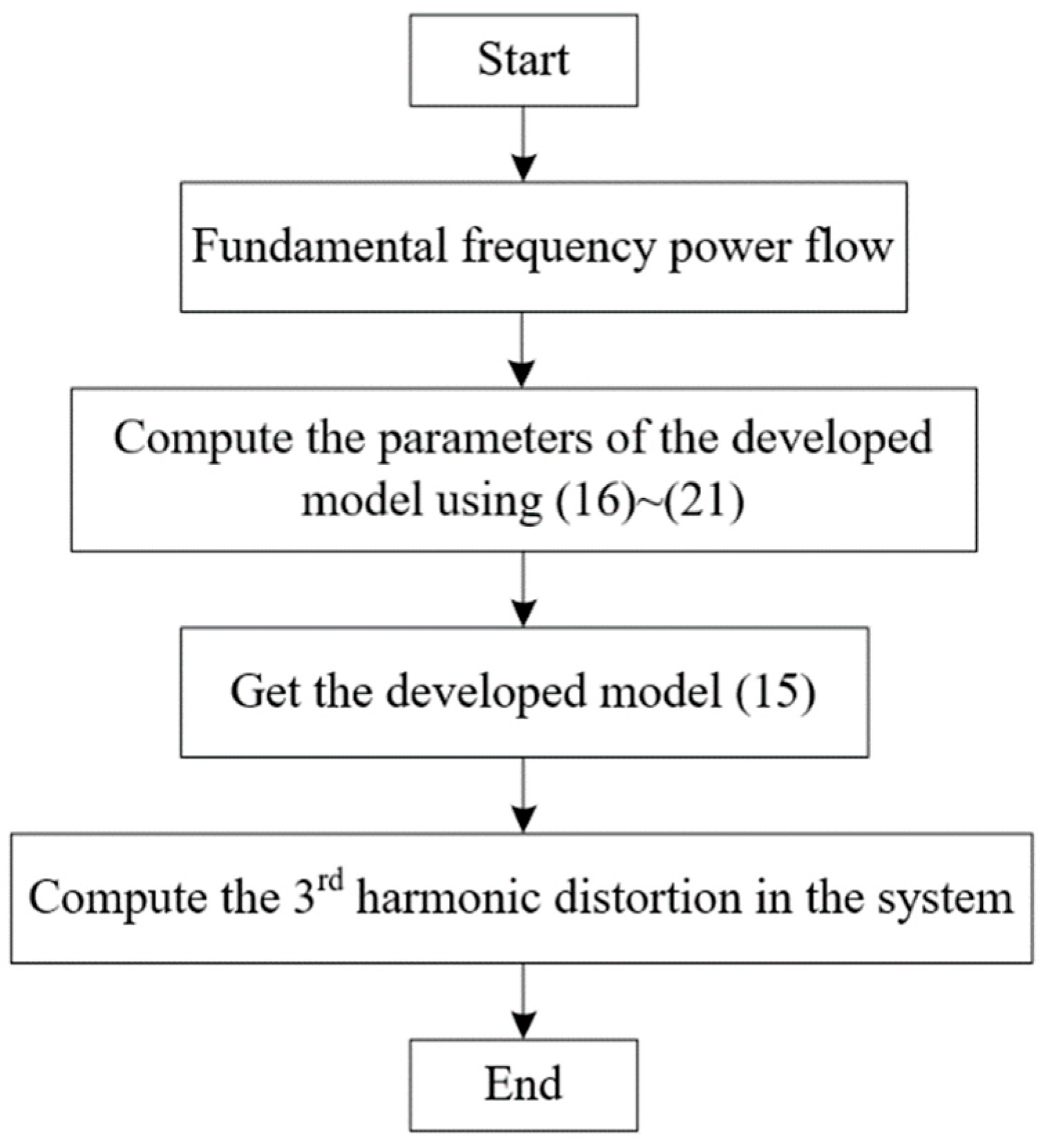
According to the above results, the fundamental frequency components are needed to complete the developed model. For this purpose, the load flow methods regarding the unbalanced power systems with VSC devices are needed. At present, numerous works have been conducted on this aspect [20,21,22,23]. These methods can be used to compute the positive-sequence and negative-sequence fundamental frequency voltage and current. The procedure to obtain the final model of the VSC can be summarized as the flow chart in Figure 3.
Compared with other existing models, the proposed model for third harmonic computation has the following advantages:
  • The mechanism of the production of the non-characteristic third harmonics are fully revealed so that the contributions of the different components to the non-characteristic third harmonics emission can be easily analyzed. Accordingly, the control scheme that can suppress the third harmonic emission can be designed.
  • The computation of the proposed model is very easy as the analytical expression of the proposed model is given. Compared with other methods, it is more straightforward for users.
  • The proposed model can be integrated into the existing harmonic power flow tools. As a result, the non-characteristic third harmonic can be computed along with other harmonic components, which can be easily adopted by the users.

4. Verification of the Proposed Model by Time-Domain Simulations

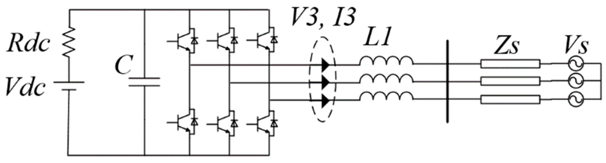
In this section, the developed model of VSC under unbalanced conditions is verified via time-domain simulations in the VSC system of Figure 4 in MATLAB/Simulink. The VSC has the same control strategy as that in Figure 1. The system parameters are listed in Table 1 [24,25]. The unbalanced condition is created by adding a negative-sequence fundamental frequency voltage in the AC source (Vs in Figure 4). Therefore, the ac voltage source can be expressed as
V s a ( t ) = V s + cos ( ω 1 t + ϕ s + ) + V s cos ( ω 1 t + ϕ s )
For illustration, the unbalanced level of the system is defined as
l = V s V s + × 100 %
The basic strategy to verify the proposed model is summarized as follows:
  • Implement the simulation system in MATLAB/Simulink, then set different unbalanced levels to run the simulations. The simulation results give the third harmonic distortion levels.
  • Based on the parameters of the simulation system and the unbalanced levels, the Thevenin circuit can be computed.
  • Once the Thevenin circuit is obtained, the third harmonic distortion levels in the system can be computed for different unbalanced levels.
  • The calculated third harmonic distortion levels are compared with the results obtained from the time-domain simulations in step (1). If these two types of results match well, then it verifies the correctness of the proposed model at third harmonics.
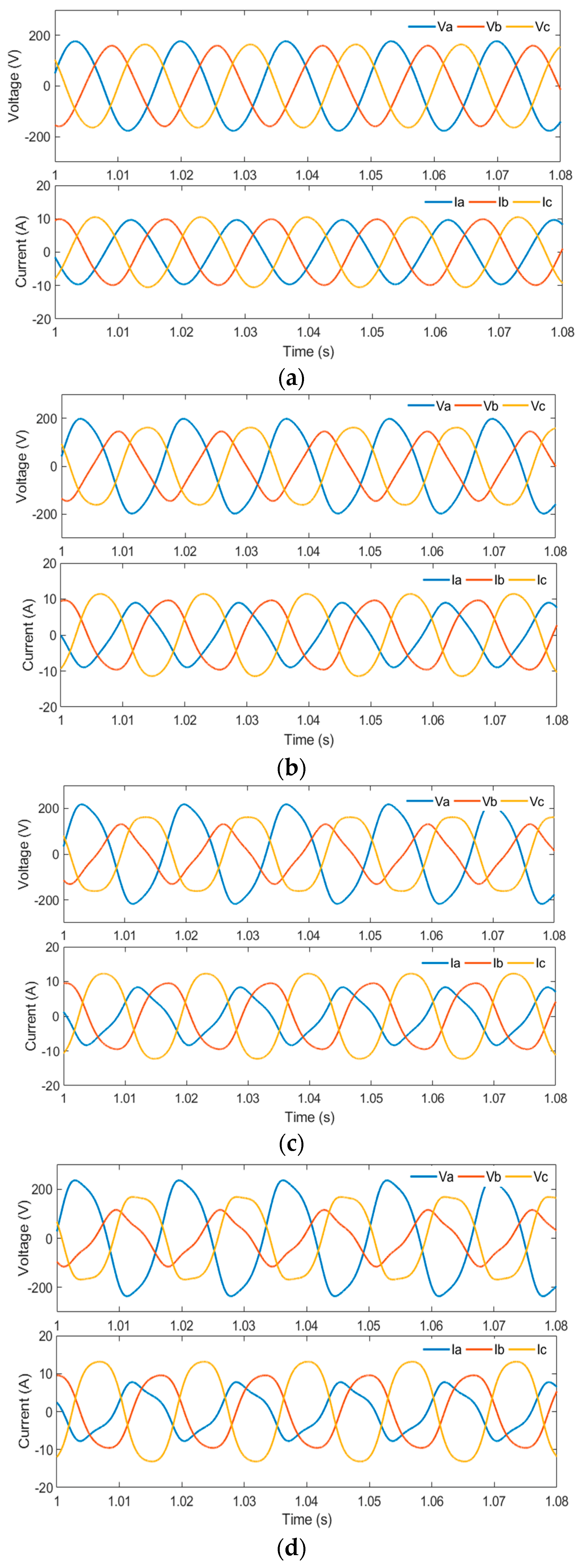
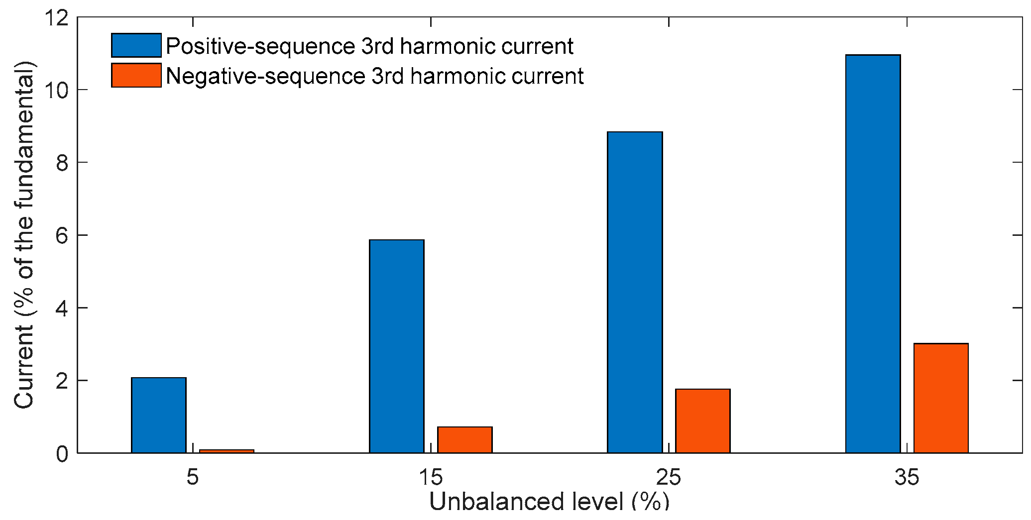
The developed third harmonic model is tested under an unbalanced level of 5%, 15%, 25%, and 35%. The simulated waveforms of the AC-side voltage and current of the VSC are presented in Figure 5. The waveforms of the VSC’s voltage and current can be used to compute the third harmonic voltage and current using FFT, and the IHDs of the third harmonics for different unbalanced levels are shown in Figure 6. It can be seen that a larger unbalanced level leads to larger third harmonics. When the unbalanced level is only 5%, the IHD of the positive-sequence third harmonic current is around 2%, while it increases to 11% when the unbalanced level rises to 35%. Additionally, one can also see that the positive-sequence third harmonic is much higher than the negative-sequence third harmonic. The reason is that, according to Equations (16)~(21), the positive-sequence third harmonic is more relevant with the positive-sequence fundamental frequency components, whereas the negative-sequence third harmonic is more relevant with the negative-sequence fundamental frequency components. As a result of the large positive-sequence third harmonic current, the coupling between the negative-sequence third harmonic and positive-sequence third harmonic current cannot be ignored.
It has been mentioned previously that, to obtain the developed model, the positive-sequence and negative-sequence fundamental frequency voltage and current are needed. In the following, the calculated positive-sequence and negative-sequence voltage and current are compared with the simulation results first, and then these values are used to compute the developed model.

4.1. Computation of the Fundamental Frequency Components

The positive-sequence and negative-sequence fundamental frequency voltage and current can be obtained through load flow studies. However, it is noted from the derived model that both the positive-sequence and negative-sequence fundamental frequency components in the modulation signal are needed to compute the developed model. Due to the control and switching process features, the positive-sequence and negative-sequence fundamental-frequency components in the modulation signal can be computed using Equations (24) and (25), respectively.
m 1 + = V 1 + / V d c 0
m 1 = H ( 2 j ω 1 ) I 1
For the studied four cases, the calculated ac-side positive-sequence fundamental frequency voltage and negative-sequence fundamental frequency current and modulation signals regarding various unbalanced levels are compared in Table 2 and Table 3. It can be seen that the calculated fundamental frequency components under various unbalanced conditions match well with the simulated results. Based on the obtained positive-sequence voltage and the negative-sequence current, the corresponding modulation signal can be computed using (24) and (25).

4.2. Verification of the Proposed Model

According to the obtained fundamental frequency components above, the parameters of the developed model in (15) can be computed, and the parameters of this model for different unbalanced levels are listed in Table 4. It can be seen that, since the positive-sequence third harmonic current is much larger than the negative-sequence third harmonic current, the coupling between the negative-sequence third harmonic voltage and the positive-sequence third harmonic current is more important. According to the calculated parameters, the third harmonic current can be computed using the following equation:
V s 3 + V s 3 = Z 3 + Z 3 + , 3 Z 3 , 3 + Z 3 I 3 + I 3 + Z L 1 + Z L s 0 0 Z L 1 + Z L s I 3 + I 3
and the third harmonic voltage on the ac side of the VSC can be computed as
V t 3 + V t 3 = V s t 3 + V s t 3 + Z 3 + Z 3 + , 3 Z 3 , 3 + Z 3 I 3 + I 3
The comparison results between the calculated harmonic voltage and current on the ac side of the VSC for the four studied cases are listed in Table 5 and Table 6. One can see that both the calculated positive-sequence and negative-sequence third harmonic voltages match well with the simulated results, which verifies the correctness of the proposed model. In the calculations, the coupling between the positive-sequence and negative sequence third harmonics is included. This is very important for the computation for the negative-sequence third harmonics due to the large positive-sequence third harmonic current.

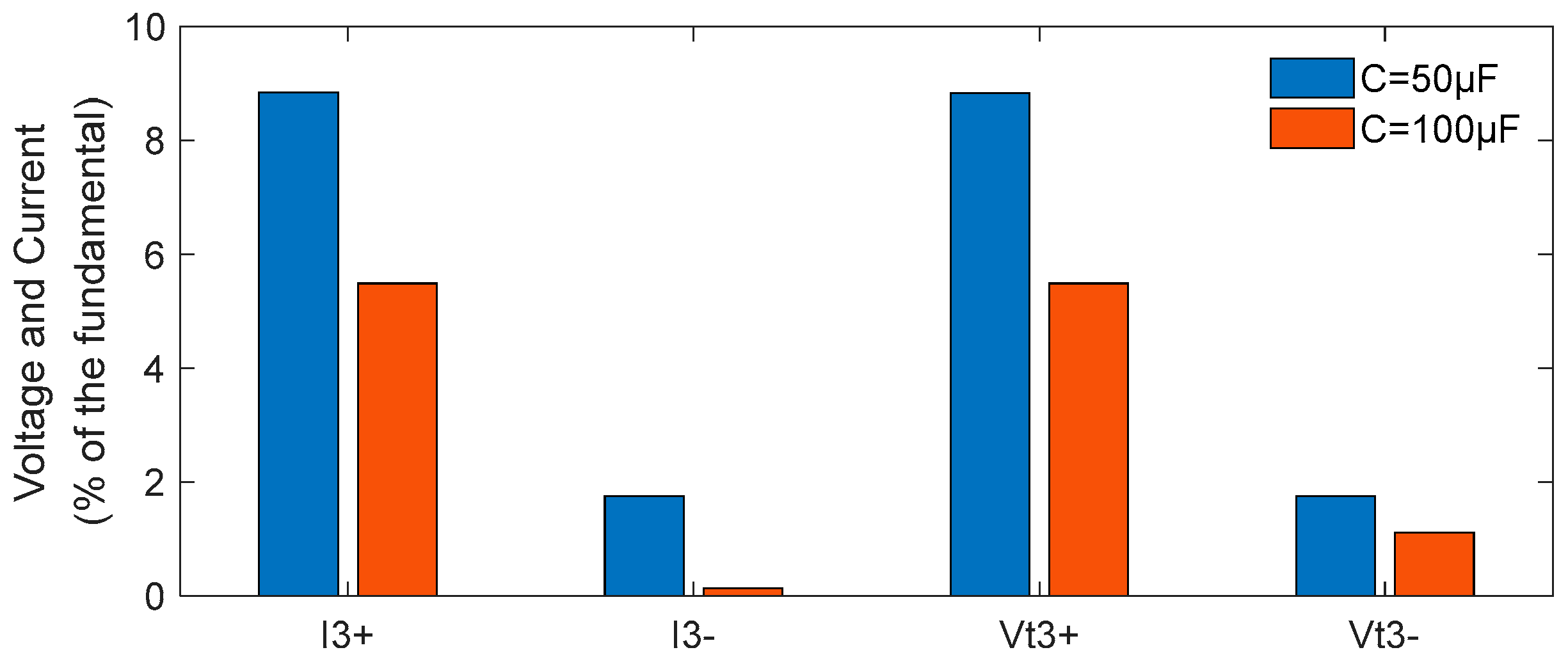
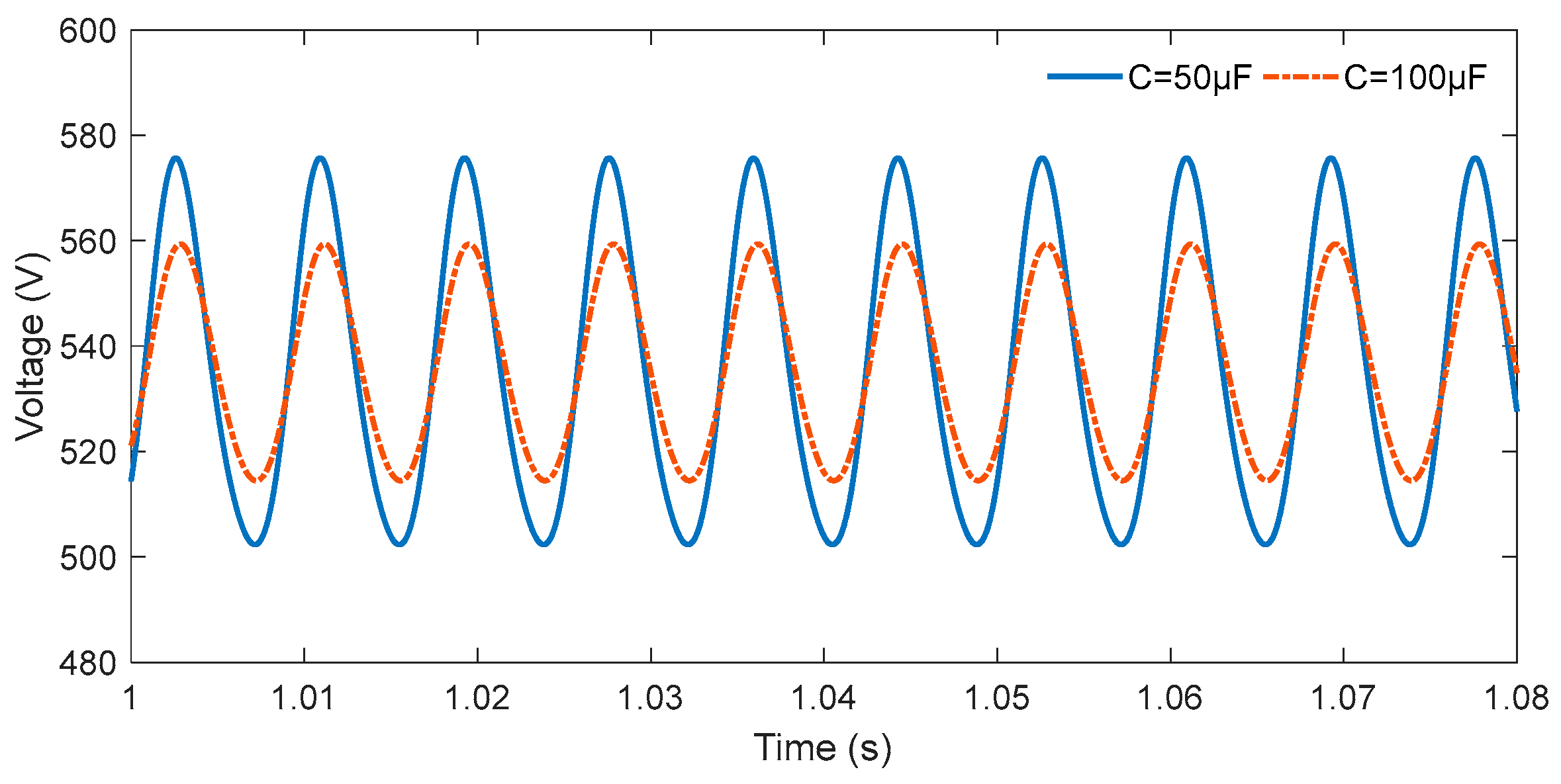
4.3. Impact of the Dc-Link Capacitor

According to the derivations in Section 2 and Section 3, the value of the DC-side capacitor plays an important role in the developed model. For the same unbalanced level, the larger the DC-side capacitor, the smaller the third harmonic. This can be verified by the simulation results in Figure 7, which are based on an unbalanced level of 25%. As one can see, when the DC-side capacitor is increased to 100 μF, the third harmonic voltage and current are significantly decreased. The results can also be supported by the harmonic voltage of the dc side, which is shown in Figure 8. It is found that the harmonic ripples (mainly second harmonics) in the dc-link voltage for a dc-link capacitor of 100 μF are much smaller than those for a dc-link capacitor of 50 μF. In summary, increasing the DC-link capacitor’s value can resist the generation of the uncharacteristic third harmonic.

5. Discussion

The above results have shown the correctness of the developed model, but it has to be pointed out that the new model can only be developed with the accurate information of the positive-sequence and negative-sequence fundamental frequency voltage and current. If these parameters cannot be provided, then the model cannot be accurately developed. It is noteworthy that the positive-sequence third harmonic distortion is much larger than the negative-sequence third harmonic. Therefore, for the evaluation of the harmonic impact, the level of the positive-sequence third harmonic is sufficient. Moreover, since the negative-sequence harmonic is quite small, its coupling effect to the positive-sequence voltage can be ignored as well. As a result, for the evaluation of the non-characteristic third harmonics, the model can be practically simplified as a Thevenin circuit, and the computation can be simplified accordingly.
The proposed model is able to show the effect of different components on the Thevenin circuit, and, thus, an optimal parameter design can be achieved to reduce the third harmonic distortion. Additionally, the proposed model can help to implement the control schemes for suppressing the third harmonic distortion caused by the VSC under unbalanced conditions.

6. Conclusions

An analytical model of VSC for calculating the non-characteristic third harmonics generated by the VSC operated under unbalanced conditions has been developed. The model is a coupled Thevenin circuit, which can be used to compute the noncharacteristic third harmonics. The correctness and effectiveness of the proposed model for computing noncharacteristic third harmonics have been verified by EMT simulations. Based on the proposed model, the findings regarding the noncharacteristic third harmonic caused by the VSC can be summarized as follows:
  • The VSC generates both positive-sequence and negative-sequence third harmonics under unbalanced conditions. The VSC can be modeled as a coupled Thevenin circuit at third harmonics. The source of the Thevenin circuit is determined by the fundamental frequency voltage and current. The impedances are determined by the control parameters and the fundamental frequency components.
  • The positive-sequence third harmonic distortion is much larger than the negative-sequence third distortion. As a result, only computing the positive-sequence third harmonic is sufficient to evaluate the impact of the VSC’s third harmonic emission under unbalanced condition.
  • The larger unbalanced levels and smaller size of the dc-link capacitor introduce a larger third harmonic current.

Author Contributions

Methodology, M.Z. and H.Z.; validation, M.Z. and H.Z.; writing, M.Z. and H.Z.; funding acquisition, H.Z. and R.F.; resources, M.Z. and S.Z.; data curation, M.Z., R.L. and J.W. All authors have read and agreed to the published version of the manuscript.

Funding

This work is supported by State Grid Shanxi Electric Power Company Science and Technology Project Research: Research and application of fusion perception and data mining technology of distribution network power quality based on smart IOT (52053020000X).

Institutional Review Board Statement

Not applicable.

Informed Consent Statement

Not applicable.

Data Availability Statement

The data are available upon request from the corresponding author.

Conflicts of Interest

The authors declare no conflict of interest.

Nomenclature

V(.)Voltage
I(.)Current
m(.)Modulation signal
ωAngular frequency
(.)aQuantities for phase A
(.)bQuantities for phase B
(.)cQuantities for phase C
(.)1+Quantities at positive-sequence fundamental frequency
(.)1−Quantities at negative-sequence fundamental frequency
(.)3+Quantities at positive-sequence third harmonic
(.)3−Quantities at negative-sequence fundamental frequency
δAngle of current
θAngle of modulation signal
(.)dcQuantities on the dc side
CDC-link capacitor
LfFront-end passive filter
H1(s)Transfer function of VSC’s inner control loop
iThe imaginary part of the plural

References

  1. Carrasco, J.M.; Franquelo, L.G.; Bialasiewicz, J.T.; Galvan, E.; Portillo, R.; Prats, M.M.; Leon, J.I.; Moreno-Alfonso, N. Power-electronic systems for the grid integration of renewable energy sources: A survey. IEEE Trans. Ind. Electron. 2006, 53, 1002–1016. [Google Scholar] [CrossRef]
  2. Segundo-Ramirez, J.; Medina, A. Modeling of FACTS Devices Based on SPWM VSCs. IEEE Trans. Power Del. 2009, 24, 1815–1823. [Google Scholar] [CrossRef]
  3. Pan, E.; Yue, B.; Li, X.; Zhao, Z.; Zhu, Q. Integration technology and practice for long-distance offshore wind power in China. Energy Convers. Econ. 2020, 1, 4–19. [Google Scholar] [CrossRef]
  4. Arazi, M.; Payman, A.; Camara, M.B.; Dakyo, B. Bidirectional Interface Resonant Converter for Wide Voltage Range Storage Applications. Sustainability 2022, 14, 377. [Google Scholar] [CrossRef]
  5. Sirjani, R. Optimal Capacitor Placement in Wind Farms by Considering Harmonics Using Discrete Lightning Search Algorithm. Sustainability 2017, 9, 1669. [Google Scholar] [CrossRef] [Green Version]
  6. Rao, S.N.V.B.; Kumar, Y.V.P.; Pradeep, D.J.; Reddy, C.P.; Flah, A.; Kraiem, H.; Al-Asad, J.F. Power Quality Improvement in Renewable-Energy-Based Microgrid Clusters Using Fuzzy Space Vector PWM Controlled Inverter. Sustainability 2022, 14, 4663. [Google Scholar] [CrossRef]
  7. Iqbal, M.N.; Kütt, L.; Daniel, K.; Asad, B.; Ghahfarokhi, P.S. Estimation of Harmonic Emission of Electric Vehicles and Their Impact on Low Voltage Residential Network. Sustainability 2021, 13, 8551. [Google Scholar] [CrossRef]
  8. Blasko, V.; Kaura, V. A new mathematical model and control of a three-phase AC-DC voltage source converter. IEEE Trans. Power Electron. 1997, 12, 116–123. [Google Scholar] [CrossRef]
  9. Torquato, R.; Hax, G.R.T.; Freitas, W.; Nassif, A. Impact Assessment of High-Frequency Distortions Produced by PV Inverters. IEEE Trans. Power Del. 2021, 36, 2978–2987. [Google Scholar] [CrossRef]
  10. Yazdani, A.; Iravani, R. A unified dynamic model and control for the voltage-sourced converter under unbalanced grid conditions. IEEE Trans. Power Del. 2006, 21, 1620–1629. [Google Scholar] [CrossRef]
  11. Kamh, M.Z.; Iravani, R. Unbalanced Model and Power-Flow Analysis of Microgrids and Active Distribution Systems. IEEE Trans. Power Del. 2010, 25, 2851–2858. [Google Scholar] [CrossRef]
  12. Karimi, H.; Karimi-Ghartemani, M.; Sheshyekani, K. Robust Control of Three-Phase Voltage Source Converters under Unbalanced Grid Conditions. IEEE Trans. Power Electron. 2019, 34, 11278–11289. [Google Scholar] [CrossRef]
  13. Merritt, N.R.; Chakraborty, C.; Bajpai, P. New Voltage Control Strategies for VSC-Based DG Units in an Unbalanced Microgrid. IEEE Trans. Sustain. Energy 2017, 8, 1127–1139. [Google Scholar] [CrossRef]
  14. Hwang, J.G.; Lehn, P.W.; Winkelnkemper, M. Control of grid connected AC-DC converters with minimized DC link capacitance under unbalanced grid voltage condition. In Proceedings of the 2007 European Conference on Power Electronics and Applications, Aalborg, Denmark, 2–5 September 2007; pp. 1–10. [Google Scholar]
  15. Lo, Y.H.; Chen, Y.C.; Lian, K.L.; Karimi, H.; Wang, C.Z. An Iterative Control Method for Voltage Source Converters to Eliminate Uncharacteristic Harmonics Under Unbalanced Grid Voltages for High-Power Applications. IEEE Trans. Sustain. Energy 2019, 10, 1419–1429. [Google Scholar] [CrossRef]
  16. Zhong, Q.; Lin, L.X.; Wang, G.; Zhang, Y.; Wu, Z.G. Harmonic analysis model for voltage source converter under unbalanced conditions. IET Gener. Transm. Distrib. 2015, 9, 12–21. [Google Scholar] [CrossRef]
  17. Nascimento, C.F.; Watanabe, E.H.; Dietrich, A.B.; Dias, R.F.S.; Diene, O. Non-Characteristic Harmonics and DC Side Capacitor Calculation in VSC Connected to a Distribution System with Unbalanced Voltage. In Proceedings of the 2015 IEEE 24th International Symposium on Industrial Electronics (ISIE), Buzios, Brazil, 3–5 June 2015; pp. 349–354. [Google Scholar]
  18. Nascimento, C.F.; Watanabe, E.H.; Diene, O.; Dietrich, A.B.; Goedtel, A.; Gyselinck, J.J.C.; Dias, R.F.S. Analysis of Noncharacteristic Harmonics Generated by Voltage-Source Converters Operating under Unbalanced Voltage. IEEE Trans. Power Del. 2017, 32, 951–961. [Google Scholar] [CrossRef]
  19. Gao, B.; Wang, Y.; Xu, W. Modeling Voltage Source Converters for Harmonic Power Flow Studies. IEEE Trans. Power Del. 2021, 36, 3426–3437. [Google Scholar] [CrossRef]
  20. Gao, B.; Wang, Y.; Xu, W. An Improved Model of Voltage Source Converters for Power System Harmonic Studies. IEEE Trans. Power Del. 2021. early access. [Google Scholar] [CrossRef]
  21. Khushalani, S.; Solanki, J.M.; Schulz, N.N. Development of three-phase unbalanced power flow using PV and PQ models for distributed generation and study of the impact of DG models. IEEE Trans. Power Syst. 2007, 22, 1019–1025. [Google Scholar] [CrossRef]
  22. AlHajri, M.F.; El-Hawary, M.E. Exploiting the Radial Distribution Structure in Developing a Fast and Flexible Radial Power Flow for Unbalanced Three-Phase Networks. IEEE Trans. Power Del. 2010, 25, 378–389. [Google Scholar] [CrossRef]
  23. Wang, Y.; Zhang, N.; Li, H.; Yang, J.W.; Kang, C.Q. Linear Three-Phase Power Flow for Unbalanced Active Distribution Networks with PV Nodes. CSEE J. Power Energy Syst. 2017, 3, 321–324. [Google Scholar] [CrossRef]
  24. Yazdani, A.; Iravani, R. Voltage-Sourced Converter in Power Systems: Modelling, Control, and Application; Wiley: New York, NY, USA, 2010. [Google Scholar]
  25. Liserre, M.; Blaabjerg, F.; Dell’Aquila, A. Step-by-step design procedure for a grid-connected three-phase PWM voltage source converter. Int. J. Electron. 2004, 91, 445–460. [Google Scholar] [CrossRef]
Figure 1. The VSC for unbalanced condition illustration. (a) VSC. (b) Control of the VSC.
Sustainability 14 06449 g001
Figure 3. Procedure to compute the noncharacteristic third harmonics under the unbalanced condition.
Sustainability 14 06449 g003
Figure 4. The VSC for unbalanced condition illustration.
Sustainability 14 06449 g004
Figure 5. Voltage and current waveforms on the ac side of the VSC under different unbalanced levels. (a) l = 5%. (b) l = 15%. (c) l = 25%. (d) l = 5%.
Sustainability 14 06449 g005
Figure 6. IHDs of the third harmonic on the ac side of the VSC.
Sustainability 14 06449 g006
Figure 7. Impact of the size of the dc-link capacitor.
Sustainability 14 06449 g007
Figure 8. Waveforms of the dc-link voltage for different dc-link capacitors.
Sustainability 14 06449 g008
Table 1. System parameters.
ParameterValueParameterValue
fswitch3 kHzVs200 V
L15 mLLs10 mL
Kp0.023Ki43.15
C50 μFVdc600 V
Rdc60 ΩNominal P1 kW
Table 2. Results of the positive-sequence fundamental frequency voltage.
Unbalanced Level (l)Simulated Vt1+Calculated Vt1+
5%0.9815 −70.9336°0.982 −70.9159°
15%0.982 −70.8655°0.982 −70.9159°
25%0.9829 −70.7298°0.982 −70.9159°
35%0.9842 −70.5274°0.982 −70.9159°
Table 3. Results of the positive-sequence fundamental frequency current.
Unbalanced Level (l)Simulated I1−Calculated I1−
5%−0.0137 − 0.0419i−0.0137 − 0.0420i
15%−0.0387 − 0.1233i−0.0410 − 0.1259i
25%−0.0586 − 0.1989i−0.0540 − 0.1998i
35%−0.0739 − 0.2677i−0.0756 − 0.2797i
Table 4. Computed impedance and source.
lZ3+Z3−Z3+,3−Z3−,3+V3t+V3t
5%7.73 − 14.86i6.44 − 7.87i0.13 − 0.12i0.03 − 0.22i−1.58 + 0.50i−0.06 + 0.09i
15%7.84 − 15.26i6.56 − 8.1i0.37 − 0.35i0.11 − 0.64i−4.48 + 1.3i−0.57 + 0.75i
25%8.13 − 16.1i6.84 − 8.55i0.55 − 0.55i0.21 − 0.98i−6.82 + 1.76i−1.53 + 1.79i
35%8.07 − 16.3i6.78 − 8.62i0.69 − 0.71i0.33 − 1.25i−8.6 + 1.93i−2.86 + 2.97i
Table 5. Test results of the developed model for voltage.
Unbalanced Level (l)Positive-Sequence Third Harmonic Voltage Using Time-Domain SimulationsPositive-Sequence Third Harmonic Voltage Using Proposed Model
5%0.1742 − 0.113i0.1745 − 0.1106i
15%0.5131 − 0.284i0.5141 − 0.2761i
25%0.8169 − 0.3377i0.8187 − 0.3189i
35%1.058 − 0.2822i1.0573 − 0.2508i
Unbalanced Level (l)Negative-Sequence Third Harmonic Voltage Using Time-Domain SimulationsNegative-Sequence Third Harmonic Voltage Using Proposed Model
5%0.0008 − 0.0086i0.0008 − 0.0086i
15%0.0088 − 0.071i0.0088 − 0.071i
25%0.0278 − 0.1733i0.0286 − 0.1736i
35%0.0574 − 0.2959i0.0589 − 0.2956i
Table 6. Test results of the developed model for current.
Unbalanced Level (l)Positive-Sequence Third Harmonic Voltage Using Time-Domain SimulationsPositive-Sequence Third Harmonic Voltage Using Proposed Model
5%−1.9172 − 2.9548i−1.9124 − 2.9669i
15%−4.8182 − 8.7052i−4.7920 − 8.7518i
25%−5.7287 − 13.8587i−5.6458 − 14.1981i
35%−4.7867 − 17.9513i−4.6459 − 17.5674i
Unbalanced Level (l)Negative-Sequence Third Harmonic Voltage Using Time-Domain SimulationsNegative-Sequence Third Harmonic Voltage Using Proposed Model
5%−0.1456 − 0.0139i−0.1466 − 0.0136i
15%−1.2053 − 0.1488i−1.2154 − 0.1488i
25%−2.9408 − 0.4724i−2.9901 − 0.5058i
35%−5.0207 − 0.9740i−5.0250 − 0.9508i
Publisher’s Note: MDPI stays neutral with regard to jurisdictional claims in published maps and institutional affiliations.

