Article

Enhancing the Performance of an Sb2Se3-Based Solar Cell by Dual Buffer Layer

1
Academy of Scientific and Innovative Research (AcSIR), Ghaziabad 201002, India
2
Indian Reference Materials (BND) Division, CSIR-National Physical Laboratory, K. S. Krishnan Marg, New Delhi 110012, India
*
Authors to whom correspondence should be addressed.
Sustainability 2021, 13(21), 12320; https://doi.org/10.3390/su132112320
Submission received: 22 September 2021 / Revised: 26 October 2021 / Accepted: 3 November 2021 / Published: 8 November 2021
(This article belongs to the Special Issue Green Energy Technologies for Sustainability)

Abstract

:
In an Sb2Se3-based solar cell, the buffer layer is sandwiched between the absorber and the window layer, playing an essential role in interfacial electricity. Generally, CdS is used as a buffer layer, but its toxic nature and low bandgap can cause current loss because of parasitic absorption. In this work, we optimized the buffer layer by using ZnS as an alternative to the CdS buffer layer in order to decrease the use of CdS. The effect of different buffer layers on the solar device was explored by numerical simulation with the help of SCAPS 1D software. The basic parameters, such as open-circuit voltage (Voc), current density (Jsc), fill factor (FF), and efficiency (η) were analyzed and compared for both the buffer layers (CdS/ZnS). The results demonstrate that changing buffer materials and thicknesses has a significant impact on cell performance. The efficiency for the ZnS buffer layer was lower compared to that of the CdS-based solar cells because of insufficient energy band alignment. In order to enhance the efficiency of Sb2Se3-based solar cells, we used CdS/ZnS dual buffer layers and studied the device performance. The work function of the back contact also affects the device performance, and for work functions below 4.8 eV, the device’s efficiency was very low. The effect of varying the thicknesses and temperatures of the buffer layers on the I-V/C-V characteristics, quantum efficiency, and energy band structure are also reported. This study shall guide the researcher in reducing CdS and improving the device’s performance.

1. Introduction

Energy is a critical component of social and economic development. The objective of energy transformation is to increase access to energy in order to improve productivity. Solar cells have been identified as a feasible alternative for solving the energy shortage and reducing the environmental problems arising from fossil fuels. The antimony selenide (Sb2Se3)-based solar cell is a recent addition to the family of thin-film photovoltaics, as it is a promising material, having an optimal bandgap (1.2 eV) [1], a high absorption coefficient (>105 cm−1) [2], and a low cost. Both Sb and Se are abundant on the earth, cheap, and nontoxic. As a result, Sb2Se3 will be a viable photovoltaic material in the future. For the first time, in 2009, Messina et al., prepared the Sb2Se3 as an absorber layer for a solar cell by chemical bath deposition (CBD) and achieved 0.66% efficiency [3]. In 2014, Zhou et al., and Luo et al., fabricated the Sb2Se3-based device by spin coating and the thermal evaporation method, and reported efficiencies of 2.26% and 1.9%, respectively [2,4]. In 2018, Wen et al., deposited the Sb2Se3 thin film by the vapor deposition method (VTD) and achieved an efficiency of 7.6% [5]. The next year, Li et al., used the closed-space sublimation [CSS] method to grow the Sb2Se3 nanorod and achieved an efficiency of 9.2% [6]. A few parameters must be examined in order to enhance the device’s performance, which puts a massive load on experimental research. Theoretical calculations provide a rapid and efficient approach for investigating these key parameters, leading to valuable practical suggestions.
The buffer/absorber interface has been the subject of several articles and is used to enhance the heterojunction and interface qualities [7,8]. Sb2Se3 is an effective photovoltaic absorber that has an improved power conversion efficiency (PCE) [9]. The solar cell absorber layer must fulfill three critical criteria: (i) a significant absorption coefficient within the spectrum region, allowing photons to be efficiently absorbed and electron–hole pairs to be generated; (ii) excellent charge-carrier transport characteristics for harvesting photogenerated carriers before recombination; (iii) a strong and consistent internal electric field within the junction in order to ensure electron–hole pair separation [10].
In a solar cell, because of the formation of a built-in electric field at the p-nheterojunction between the Sb2Se3/CdS interface, photogenerated electrons flow from p-type Sb2Se3 to n-type CdS, and then into the transparent electrode (TE) layer. The p-type hole-transport layer, on the other hand, attracts holes, which the back contact collects. Various parameters, such as open-circuit voltage (Voc), the current density (Jsc), the fill factor (FF), and the efficiency (η) show the device’s performance. The highest voltage developed in a solar cell at zero current is called “open-circuit” voltage, and it is affected by the temperature, as revealed by Equation (1):
V o c = n k T q l n I L I 0 + 1
Here, IL and I0 are light-generated and dark saturation currents, respectively; q is the charge; and T is the temperature. The Voc decreases by increasing the temperature.
A fill factor, FF, determines the maximum power generated from a solar cell by measuring the squareness of the current density–voltage curve. The FF can be defined by Equation (2):
F F = P M P V O C X I S C
Here, PMP is the maximum power, and ISC is the short-circuit current.
In this work, for the simulation of the ZnO/ZnS or CdS/Sb2Se3/Au solar devices, we used the SCAPS 1D software [11]. By varying the buffer layer thickness and back contact metal work function, various parameters, such as the Voc, the Jsc, the FF, and the η changed. The effects on the IV and CV characteristics and the quantum efficiency (QE), and the energy band structure results have been systematically studied. The Voc, Jsc, FF, and η are also affected by varying the device temperature (280–380 K). We have used the ZnS buffer layer as an alternative to the CdS layer because ZnS is a more efficient layer than other buffer layers, such as ZnO [12], ZnSe [13], SnO2 [14], TiO2 [15], etc., as ZnS has a wide direct bandgap of 3.5–3.8 eV. The wide bandgap provides a high optical transparency of >94% in the visible and infrared regions of the solar spectrum, and a high absorption coefficient in the ultraviolet region [16]. It is also nontoxic. The higher bandgap energy of ZnS, compared to CdS, can enhance the blue response of the photovoltaic cells by reducing the photon absorption loss.

2. Device Model and Simulation Parameters

2.1. Device Model

The present work is a simulation of a ZnO/ZnS CdS/Sb2Se3/Au solar device under AM 1.5 G and 100 mW/cm2 illumination, where ZnO is used as a window layer, ZnS/CdS as the buffer layers, Sb2Se3 as an absorber layer, and Au as a back contact metal, as shown in Figure 1.
SCAPS 1D software uses the Poisson Equation (3), continuity equations ((4) and (5)), and carrier transport equations ((6) and (7)) for electrons and holes in order to obtain the current density-voltage (JV) characteristics:
Δ ·   ε Δ ϕ = q   ( p n + N D + N A )
Δ ·   J n = q   ( R G ) + q n t
Δ ·   J p = q   ( R G ) + q p t
J n = D n d n d x + µ n n d ϕ d x
J p = D p d p d x + µ p p d ϕ d x
Here, ε is the dielectric constant; ϕ is the electrostatic potential; ND and NA are the donor and acceptor densities, respectively; p and n are the free holes and free electrons, respectively; and Jn and Jp are the current densities for the electrons and the holes, respectively. R and G are the recombination and generation rates, respectively. SCAPS divides a solar cell structure into slabs and main grid points, and the above differential equations are discretized into the algebraic equation set.
Appropriate boundary conditions at the interfaces and contacts produces a system of coupled differential equations. The meshing algorithm of this software provides coarse meshing in the middle of the layer, and finer meshing near the interface and contacts. The mesh can be optimized during the calculations. It is easy to optimize the mesh at each iteration step during simulations with the effects of the gradings, multivalent defects, and impurities on the photovoltaic properties.

2.2. Simulation Parameters

The simulated parameters are presented in Table 1 and are taken from the literature and experimental results [17,18]. The buffer layer (ZnS/CdS) thickness was varied from 20 to 80 nm, and the back contact work function was varied from 4.4 to 5.2 eV. The temperature was also changed from 280 K to 380 K to check the performance of the solar cell.

3. Results and Discussion

3.1. Solar Cell Current-Voltage Characteristic

The JV characterization method can be used to obtain insight into the performance of a solar cell device. Figure 2 shows the JV characteristics of Sb2Se3-based solar cells for three different types of buffer layers (CdS, ZnS, and CdS/ZnS). The main parameters for a solar cell (Voc, Jsc, FF, and η) were extracted. Figure 2 shows a comparison between the performance of three different buffer layers. Table 2 presents the effect of various buffer layers (CdS, ZnS, and CdS/ZnS) on the main parameters of the device.
Case 1: When CdS = 80 nm and ZnS = 0
Case 2: When ZnS = 80 nm and CdS = 0
Case 3: When CdS = 20 nm and ZnS = 60 nm

3.1.1. CdS as a Buffer Layer

The buffer layers enhance the device’s performance by charge extraction and collection in a solar cell. The highly efficient solar cells consist of CdS as a buffer layer. This layer prevents the corrosion of the absorber layer caused during window layer deposition. CdS is a material with a suitable bandgap, a high-absorption coefficient, and low resistivity, that makes excellent Ohmic contact with the solar cell absorber materials. The effect of the buffer layer thickness on the performance of a solar cell was studied. The parameters of a solar cell change by varying the buffer layer thickness. By increasing the buffer layer thickness, the open-circuit voltage (Voc) decreased from 0.849 to 0.845 eV. The current density (Jsc) was also reduced because of the parasitic absorption produced by the increased thickness of the CdS buffer layer. The fill factor (FF) increased, and the efficiency (η) was reduced for a 40 nm thick buffer layer because of the decrease in the Voc and the Jsc (as shown in Figure 3).

3.1.2. ZnS as a Buffer Layer

Zinc sulfide (ZnS), which is nontoxic and has a large bandgap, is a promising material as a buffer layer in solar cell devices. By changing the thickness of the ZnS layer, all of the parameters (Voc, Jsc, FF, and η) are also changed, as shown in Figure 4. The thickness was varied up to 80 nm, and the Voc was almost the same for all thicknesses. The Jsc first increased up to a 20 nm thickness, and then the change was tiny because the bandgap of ZnS was higher and the carrier concentration was very low. When the thickness of the ZnS buffer layer was set to be zero, the fill factor and the efficiency of the device was 84.27% and 21.56%, respectively, and later, when the thickness increased to 20 nm, the fill factor (78.07%) and the efficiency (20.83%) decreased. For 20 nm and higher thicknesses, both the fill factor and the efficiency changed only by a small amount, with change in the thickness of the ZnS buffer layer, as the increased thickness of ZnS has only a minor impact on the depletion region.

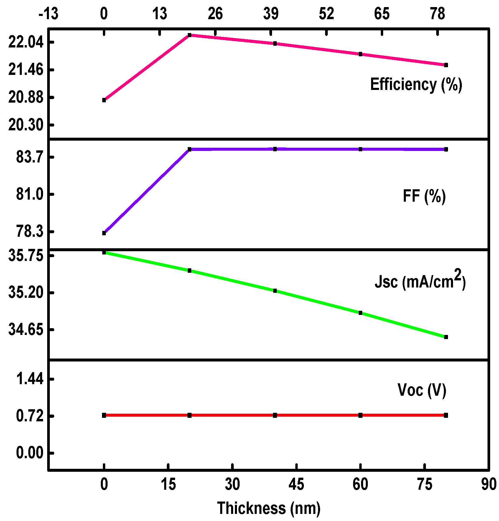
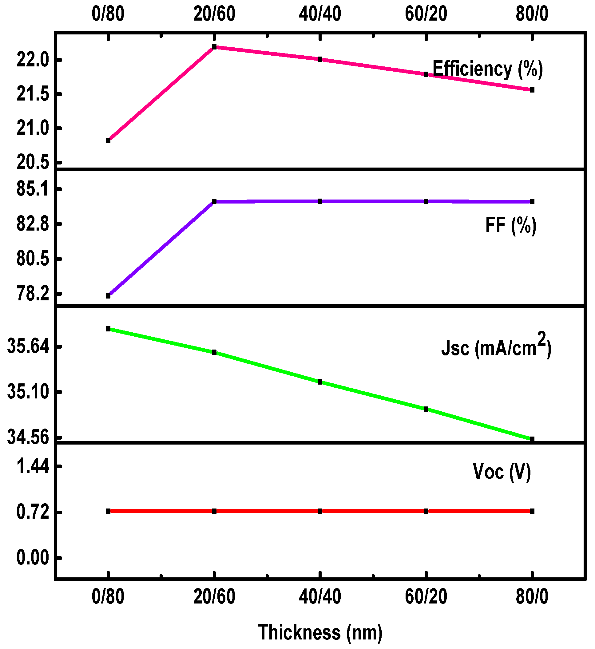
3.1.3. CdS/Zns as a Buffer Layer

A second buffer layer was added to the first buffer layer to form a dual-buffer-layered Sb2Se3 solar cell, and by changing the thickness ratio, the parameters changed, as shown in Figure 5. Here, CdS and ZnS make a dual buffer layer. The optimum thickness of CdS and ZnS are taken to be 20 nm and 60 nm, respectively, and it was observed that the FF and η values were better than those in the single-buffer-layer cases. We checked the performance of Sb2Se3-based solar cells for three different types of buffer layers. First, we used only the CdS layer with an 80 nm thickness, and the efficiency was 21.56%. In the second case, we used only the ZnS layer with an 80 nm thickness, and an efficiency of 20.82% was achieved. We used both buffer layers (CdS = 20 nm, and ZnS = 60 nm), and a maximum efficiency of 22.22% was achieved. This shows that the double buffer layer enhances the device’s performance. Although the change is nearly 1%, considering the volume of solar installation needed, it compounds to a large amount.

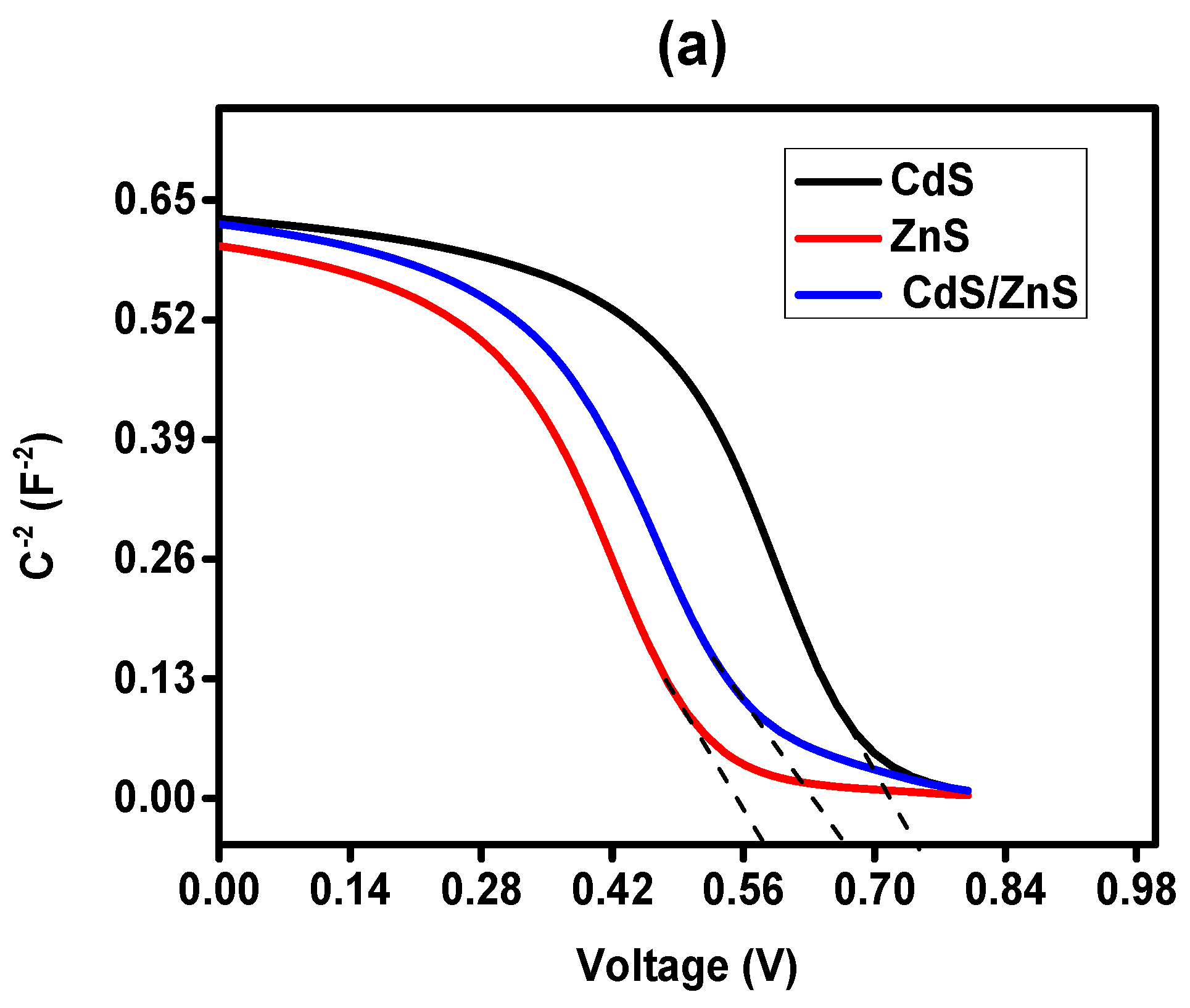
3.2. Capacitance-Voltage (CV) Characteristics

The CV characteristic [19] helps a solar device to reveal the more fundamental properties. The CV plots for three different buffer layers (CdS, ZnS, and CdS/ZnS) are studied here. The relation between the capacitance and the depletion region, NA, is given by Equation (8):
1 C 2 = 2 ( V b i V d c ) q ε A 2 N A
Here, ε is permittivity, Vbi is built-in voltage, and Vdc is the dc voltage.
A Mott–Schottky plot, obtained from the CV characteristics, is shown in Figure 6a. The measured CV curves for all three buffer layers are shown in Figure 6b. The inset of Figure 6b shows an enlarged plot. When the voltage was in the range of 0 to 0.45 eV, the capacitance value was constant for all three types of buffer layers, and, after that, the capacitance changed drastically.

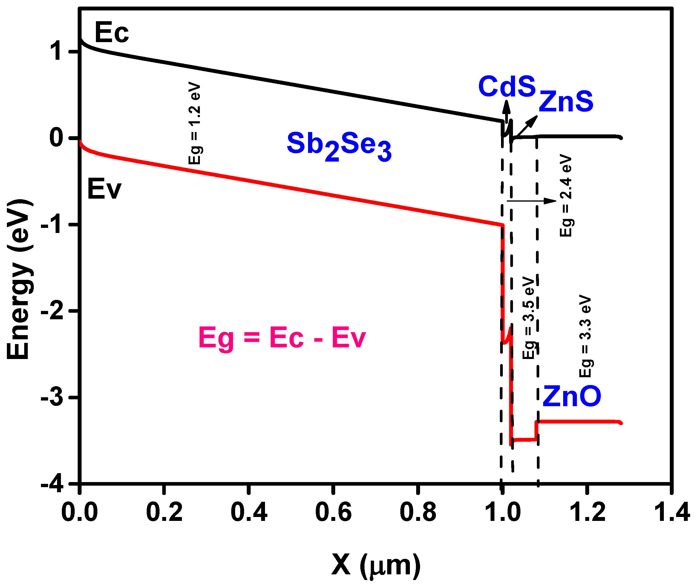
3.3. Energy Band Diagram

The energy band diagram for ZnO/CdS and ZnS/Sb2Se3/Au is shown in Figure 7. The plot is for Sb2Se3 as an absorber layer, with a thickness of 1 µm; CdS and ZnS as the buffer layers, with thicknesses of 20 nm and 60 nm, respectively; and ZnO, with a thickness of 200 nm, as a window layer. The n-type and p-type regions, and their related valence bands and conduction band edges, and the bandgap values are shown in Figure 7. When photogenerated carriers get separated at the interface between the absorber and buffer layers, the strong electric field accelerates them, causing them to be dragged away from the junction fast. The electrons move into the buffer layer, and the holes move through the absorber layer and are collected by the back contact. The band offsets are well-suited for the charge carriers, which reach the metal contact, avoiding recombination.

3.4. QE Curve

The thickness of the buffer layers (CdS, ZnS, and CdS/ZnS) affects the photon absorption and the quantum efficiency (QE), as shown in Figure 8a–c. By increasing the thickness of the CdS buffer layer, the intensity of the shortwave band decreases. This means that the thin buffer layer showed a significant band response.

3.5. Back Contact Metal Work Function

The back contacts for Sb2Se3 solar devices are metals, such as Au, Ag, Mo, Pt, etc. Molybdenum (Mo) and gold (Au) are the most often-used materials for solar cell back contacts [20]. Back contacts have the following characteristics: (i) they provide an ohmic contact [21] for connections; (ii) they are corrosion-resistant; and (iii) they have a low recombination rate for minority carriers. In this work, we have studied the effect of the work function on the various parameters (Voc, Jsc, FF, and η) at optimized conditions, as shown in Figure 9. The work function values were varied, from 4.4 to 5.2 eV, and the results show that the work function should be more significant than 4.8 eV for better efficiency. By increasing the work function, all of the parameters also increased. At 5.2 eV (for Au), the efficiency was highest (22.22%) when the buffer layer thickness was within a ratio of 20 nm:60 nm for CdS and ZnS, respectively.

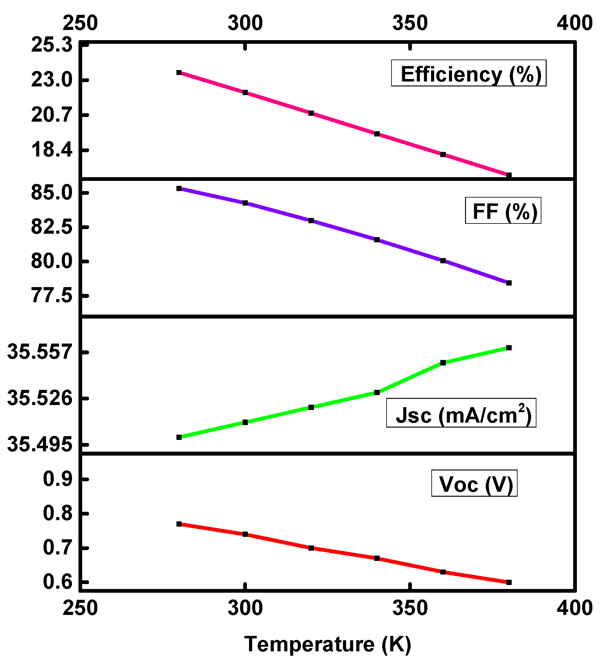
3.6. Effect of Temperature on Sb2Se3-Based Solar Device

Temperature plays a vital role in the performance of a solar cell, as the efficiency and power depend on the operating temperature. The parameters, FF, Voc, and η, decrease with increasing temperature. The parameters are presented in Table 3.
The performance decreased with an increase in the temperature from 280 to 380 K, as shown in Figure 10. The optimized parameters for the device are presented in Table 4.

4. Conclusions

The numerical simulation showed better performance for a dual buffer layer (CdS/ZnS) in a Sb2Se3-based solar device. The buffer layer thickness, temperature, and back contact metal affect various parameters, such as the Voc, the Jsc, the FF, and the efficiency. First, the device performance was checked by taking the single buffer layers of the ZnS and CdS materials. After that, the CdS/ZnS buffer layer was used to minimize the use of CdS toxic material. It was noticed that the thickness combination of 20:60 nm of the CdS/ZnS buffer layer was best-suited to achieving the highest efficiency (22.22%). ZnS is a more efficient layer than other buffer layers because of its wider bandgap. It is also nontoxic. The back contact metal work function also plays a vital role in enhancing efficiency, and the results show that the work function value should be more than 4.8 eV for better performance. At 280 K, the highest efficiency of 23.49% was achieved for Sb2Se3-based solar cells. Our simulation results can help to develop high-performance Sb2Se3 solar cells.

Author Contributions

Conceptualization, M.; methodology, M.; validation, M.; formal analysis, M.; investigation, M.; data curation, M.; writing—original draft preparation, M.; writing—review and editing, K.K.M. and V.N.S.; supervision, K.K.M. and V.N.S. All authors have read and agreed to the published version of the manuscript.

Funding

This research received no external funding.

Institutional Review Board Statement

Not applicable.

Informed Consent Statement

Not applicable.

Data Availability Statement

The data presented in this study are available on request from the corresponding author.

Acknowledgments

Mamta highly acknowledges the Council for Scientific and Industrial Research (CSIR), India, for the Senior Research Fellowship (SRF) grant. The authors would like to thank their institute for its support. The authors would like to thank Marc Burgelman of the Gent University, Belgium, for providing the SCAPS program.

Conflicts of Interest

The authors declare no conflict of interest.

References

  1. Vadapoo, R.; Krishnan, S.; Yilmaz, H.; Marin, C. Electronic structure of antimony selenide (Sb2Se3) from GW calculations. Phys. Status Solidi (b) 2011, 248, 700–705. [Google Scholar] [CrossRef]
  2. Zhou, Y.; Leng, M.; Xia, Z.; Zhong, J.; Song, H.; Liu, X.; Yang, B.; Zhang, J.; Chen, J.; Zhou, K. Solution-Processed Antimony Selenide Heterojunction Solar Cells. Adv. Energy Mater. 2014, 4, 1301846. [Google Scholar] [CrossRef]
  3. Messina, S.; Nair, M.T.S.; Nair, P.K. Antimony Selenide Absorber Thin Films in All-Chemically Deposited Solar Cells. J. Electrochem. Soc. 2009, 156, H327–H332. [Google Scholar] [CrossRef]
  4. Luo, M.; Leng, M.; Liu, X.; Chen, J.; Chen, C.; Qin, S.; Tang, J. Thermal evaporation and characterization of superstrate CdS/Sb2Se3 solar cells. Appl. Phys. Lett. 2014, 104, 173904. [Google Scholar] [CrossRef]
  5. Wen, X.; Chen, C.; Lu, S.; Li, K.; Kondrotas, R.; Zhao, Y.; Chen, W.; Gao, L.; Wang, C.; Zhang, J.; et al. Vapor transport deposition of antimony selenide thin film solar cells with 7.6% efficiency. Nat. Commun. 2018, 9, 1–10. [Google Scholar] [CrossRef] [PubMed]
  6. Li, Z.; Liang, X.; Li, G.; Liu, H.; Zhang, H.; Guo, J.; Chen, J.; Shen, K.; San, X.; Yu, W.; et al. 9.2%-efficient core-shell structured antimony selenide nanorod array solar cells. Nat. Commun. 2019, 10, 1–9. [Google Scholar] [CrossRef] [PubMed] [Green Version]
  7. Chen, C.; Zhao, Y.; Lu, S.; Li, K.; Li, Y.; Yang, B.; Chen, W.; Wang, L.; Li, D.; Deng, H.; et al. Accelerated Optimization of TiO2/Sb2Se3 Thin Film Solar Cells by High-Throughput Combinatorial Approach. Adv. Energy Mater. 2017, 7, 1700866. [Google Scholar] [CrossRef]
  8. Wang, L.; Li, D.-B.; Li, K.; Chen, C.; Deng, H.-X.; Gao, L.; Zhao, Y.; Jiang, F.; Li, L.; Huang, F.; et al. STable 6%-efficient Sb2Se3 solar cells with a ZnO buffer layer. Nat. Energy 2017, 2, 17046. [Google Scholar] [CrossRef]
  9. Mamta; Singh, Y.; Maurya, K.K.; Singh, V. A review on properties, applications, and deposition techniques of antimony selenide. Solar Energy Mater. Solar Cells 2021, 230, 111223. [Google Scholar] [CrossRef]
  10. Mavlonov, A.; Razykov, T.; Raziq, F.; Gan, J.; Chantana, J.; Kawano, Y.; Nishimura, T.; Wei, H.; Zakutayev, A.; Minemoto, T.; et al. A review of Sb2Se3 photovoltaic absorber materials and thin-film solar cells. Sol. Energy 2020, 201, 227–246. [Google Scholar] [CrossRef]
  11. Burgelman, M.; Verschraegen, J.; Degrave, S.; Nollet, P. Modeling thin-film PV devices. Prog. Photovolt. Res. Appl. 2004, 12, 143–153. [Google Scholar] [CrossRef]
  12. Mukhopadhyay, K.; Inbaraj, P.F.H.; Prince, J.J. Thickness optimization of CdS/ZnO hybrid buffer layer in CZTSe thin film solar cells using SCAPS simulation program. Mater. Res. Innov. 2019, 23, 319–329. [Google Scholar] [CrossRef]
  13. Srivastava, A.; Dua, P.; Lenka, T.; Tripathy, S. Numerical simulations on CZTS/CZTSe based solar cell with ZnSe as an alternative buffer layer using SCAPS-1D. Mater. Today Proc. 2021, 43, 3735–3739. [Google Scholar] [CrossRef]
  14. Tennakone, K.; Bandara, J.; Bandaranayake, P.K.M.; Kumara, G.R.A.; Konno, A. Enhanced Efficiency of a Dye-Sensitized Solar Cell Made from MgO-Coated Nanocrystalline SnO2. Jpn. J. Appl. Phys. 2001, 40, L732–L734. [Google Scholar] [CrossRef]
  15. Akila, Y.; Muthukumarasamy, N.; Velauthapillai, D. TiO2-based dye-sensitized solar cells. In Nanomaterials for Solar Cell Applications; Elsevier: Amsterdam, The Netherlands, 2019; pp. 127–144. [Google Scholar] [CrossRef]
  16. Tchangnwa, F.N.; Kenfack, D. Thin-Film solar cells performances optimization: Case of Cu (In, Ga) Se2-ZnS. In Solar Cells—Theory, Materials and Recent Advances; IntechOpen: London, UK, 2021. [Google Scholar] [CrossRef]
  17. Li, Z.-Q.; Ni, M.; Feng, X.-D. Simulation of the Sb2Se3 solar cell with a hole transport layer. Mater. Res. Express 2019, 7, 016416. [Google Scholar] [CrossRef]
  18. Benami, A. Effect of CZTS Parameters on Photovoltaic Solar Cell from Numerical Simulation. J. Energy Power Eng. 2019, 13, 32–36. [Google Scholar] [CrossRef]
  19. Jeevandoss, C.R.; Kumaravel, M.; Kumar, V.J. A novel method for the measurement of the C-V characteristic of a solar photovoltaic cell. IEEE Instrum. Meas. Technol. Conf. Proc. 2010, 2010, 371–374. [Google Scholar] [CrossRef]
  20. Mamta; Maurya, K.K.; Singh, V.N. Sb2Se3 versus Sb2S3 solar cell: A numerical simulation. Sol. Energy 2021, 228, 540–549. [Google Scholar] [CrossRef]
  21. Schroder, D.; Meier, D. Solar cell contact resistance—A review. IEEE Trans. Electron Devices 1984, 31, 637–647. [Google Scholar] [CrossRef]
Figure 1. Structure of Sb2Se3-based solar cell with dual buffer layers.
Sustainability 13 12320 g001
Figure 2. J-V curves for CdS, ZnS, and CdS/ZnS buffer layers.
Sustainability 13 12320 g002
Figure 3. Effect of CdS buffer layer thicknesses on various parameters (Voc, Jsc, FF, and η).
Sustainability 13 12320 g003
Figure 4. Effect of ZnS buffer layer thicknesses on various parameters (Voc, Jsc, FF, and η).
Sustainability 13 12320 g004
Figure 5. Effect of dual buffer layer on various parameters (Voc, Jsc, FF, and η) of the solar device.
Sustainability 13 12320 g005
Figure 6. (a) Mott-Schottky; (b) capacitance-voltage curves for three different buffer layers: CdS, ZnS, and CdS/ZnS.
Sustainability 13 12320 g006aSustainability 13 12320 g006b
Figure 7. Energy band diagram for ZnO/CdS + ZnS/Sb2Se3based solar cell.
Sustainability 13 12320 g007
Figure 8. The QE curve for (a) CdS; (b) ZnS; and (c) CdS/ZnS buffer layers with various thicknesses.
Sustainability 13 12320 g008
Figure 9. Effect of different back contact metal work functions on various parameters (Voc, Jsc, FF, and η).
Sustainability 13 12320 g009
Figure 10. Effect of temperature on various device parameters (Voc, Jsc, FF, and η).
Sustainability 13 12320 g010
Table 1. Various input parameters of Sb2Se3-based device with dual buffer (CdS/ZnS) layer and ZnO as the window layer.
Material ParametersZnSCdSZnOSb2Se3
Thickness (nm)VariableVariable2001000
Band gap (eV)3.52.43.31.2
Electron affinity (eV)4.54.24.44.04
Dielectric permittivity1010918
CB effective density of states (1/cm3)1.5 × 10182.2 × 10182.2 × 10182.2 × 1018
VB effective density of states (1/cm3)1.8 × 10181.8 × 10191.8 × 10191.8 × 1019
Electron thermal velocity (cm/s)1.0 × 1071.0 × 1071.0 × 1071.0 × 107
Hole thermal velocity (cm/s)1.0 × 1071.0 × 1071.0 × 1071.0 × 107
Electron mobility (cm2/Vs)5010010015
Hole mobility (cm2/Vs)2025255.1
Shallow uniform donor density ND (1/cm3)1.0 × 10181.0 × 10171.0 × 10180
Shallow uniform acceptor density NA (1/cm3)0001.0 × 1013
Table 2. Effect of various buffer layers on the device parameters.
CdSZnSCdS/ZnS
Voc (V)0.7390.7420.740
Jsc (mA/cm2)34.5435.8535.57
FF (%)84.2778.0784.27
η (%)21.5620.8222.22
Table 3. Effect of temperature on various parameters (Voc, Jsc, FF, and η).
Temperature (K)Parameters
Voc (V)Jsc (mA/cm2)FF (%)η (%)
2800.7735.5085.3223.49
3000.7435.5184.2722.22
3200.7035.5282.9820.83
3400.6735.5381.5819.47
3600.6335.5580.0618.12
3800.6035.5678.4416.77
Table 4. Optimized device parameters and their values for Sb2Se3-based solar cells.
Optimized ParametersValues
Absorber layer thickness1000 nm
CdS buffer layer thickness20 nm
ZnS buffer layer thickness60 nm
Window layer thickness200 nm
Back contact work function5.2 eV
Publisher’s Note: MDPI stays neutral with regard to jurisdictional claims in published maps and institutional affiliations.

