Article

A Battery Cell Equalisation System Based on a Supercapacitors Tank and DC–DC Converters for Automotive Applications

by
Borislav Dimitrov
* and
Sylvia Konaklieva
School of Engineering, Warwick University, Coventry CV2 2DX, UK
*
Author to whom correspondence should be addressed.
World Electr. Veh. J. 2023, 14(7), 185; https://doi.org/10.3390/wevj14070185
Submission received: 13 June 2023 / Revised: 7 July 2023 / Accepted: 10 July 2023 / Published: 13 July 2023

Abstract

:
A battery cell equalisation system for automotive applications based on a supercapacitors energy storage SCES tank is proposed. The main advantages of the developed system are the utilisation of the regenerative brake energy for battery cell equalisation, reduction in the number of DC–DC converters, the flexible operation expressed by the possibility to address each battery cell with bi-directional switches, and acceptable efficiency in all modes of operation. The energy transfer between the SCES and battery cells is precisely analysed with modelling and simulations in steady-state and transient conditions. Power loss is estimated per sub-system, systemising the loss reduction techniques and achieving the maximum efficiency. The required DC–DC converters are described and designed according to the specific modes of operation in the developed application. Finally, the experimental verification is provided using a small physical model.

1. Introduction

The battery pack is an electric vehicle’s (EV) most expensive and sensitive part. Usually, it consists of hundreds or thousands of battery cells connected as a pack in series in parallel. As the cells are complex electrochemical elements, they have differences in their parameters which progress further due to temperature, charge–discharge cycles, environmental differences, etc. This leads to different cell capacitances, voltage, and self-discharge rates, eventually leading to battery pack performance and lifetime expectancy degradation. Because of this, the proposed Battery Cell Equalisation System (BCES) is a vital part of battery storage (BS).
The battery cell equalisation techniques have been an object of research in numerous studies in recent years [1,2,3,4,5,6]. The review of the primary equalisation circuits in [1] presents and compares capacitive and inductive energy storage, single and multi-tube flyback, and different DC–DC converter topologies. As the study concludes, further improvements to the battery cell equalisation system must be focused on circuit design, giving a reliable system; flexibility improvement, leading to easy expansion on a large scale; and overall efficiency increase. A widely used circuit for equalisation is inductor-based, presented in better detail in [2,3], which usually requires a significant number of inductors and completes the energy transfer between adjacent cells only. A review and comparison study [2] of the inductor-based topologies suggests universal control equalisation algorithms. Some studies present the operation of an inductor equalisation circuit developed further to a dual interleaved inductor equalisation circuit [3]. As a primary benefit, the study reports an equalisation efficiency improvement of 4.89% and a time reduction of 37.4% based on an adaptive fuzzy neural network equalisation algorithm. Further efficiency and equalisation time improvements are found using zero voltage switching quasi-resonant converters [4], giving an efficiency improvement of 6%.
Other types of battery cell equalisation systems [5,6,7,8,9] are based on the primary type switching capacitors circuits—switched capacitor and single-switched capacitor [5,6,7], modularised switched capacitor [8], and double-tiered switched capacitor [9]. These topologies require bi-directional switches. The capacitors could be high-capacitance electrolytic types. As shown in [5], a capacitor with 22   m F , E S R = 65   m Ω is successfully used to equalise two cells with initial SoC of 35% and 11.3%, or with a SoC difference of 23.7% for 545   m A h cells. Results based on simulations with a single-switched SC are given in [6], where the capacitor capacitance is raised to 16   F and E S R = 200   m Ω . Similarly, the suggested system in [7] is based on 350   F SCs with E S R = 20   m Ω . The energy storage in the SCs enough for one equalisation cycle is E = 3291.8   J , reaching an efficiency of 98.4%. As the bi-directional switches are a vital part of the equalisation system, determining the overall loss and eventually the overall efficiency, the authors in [8] suggested a circuit with a reduced number of transistors. The system efficiency varies in the 98.5–99.2% range, which is confirmed in [9].
The combination of the battery pack and SCs energy storage has also been an object of significant research as it gives substantial advantages. One advantage is the battery lifetime expectancy extension, which leads to significant financial benefits [10]. The split of the energy, delivered from both types of storage, requires precise control systems [11,12,13] with algorithms to control bi-directional [10,11] and unidirectional [13] DC–DC converters. The battery–SCs energy system efficiency could be improved by 16%, as suggested in [12], and the current throughput of the battery could be reduced by 30%. The same system’s topology is used successfully in powerful renewable energy applications [14,15,16], leading to the mitigation of power fluctuation [14] and overall system cost minimisation [15]. Also, in a range of high-power applications, SCs energy tanks are used in the railway reverse recovery storage system with an installed power of 3.5   M W , accumulating an energy value of 210   M J [16]. The system is based on bi-directional buck–boost converters, using the fast charge ability of the SCs, also depicted in [17] and relatively high efficiency proven in [18,19]. Eventually, these SCs applications show that they could be used as energy storage for battery cell equalisation, as suggested in [20]. In addition to this, considering the SCs’ mature integration [10,11] and control in the EVs Battery-SCs energy storage [12,13,14], overall financial benefits [15,16], and fast charging abilities and energy fluctuation mitigation [17,18,19], it could be suggested that the SCs energy tank could be used as a part of the battery cell equalisation system [20] further developed to utilise the regenerative brake energy from the electric drivetrain.
The comprehensive review in [21] shows the current development and application of carbon nanotubes (CNT) in the supercapacitor’s structure, significantly improving their mechanical, electrical and surface area properties. As the research describes, the CNT supercapacitors based on CNTs/graphene, CNTs/metal, and CNTs/polymer electrodes are good candidates for energy storage systems, where the CNTs/metal-based supercapacitors have the potential to achieve a higher energy density of 80 Wh/kg.
The SCES requires modelling and simulation procedures to be completed as part of the design methodology, giving the energy distribution, state of the charge, power loss and thermal conditions. As suggested in [22,23], the SCs models could be based on equivalent circuits with satisfactory precision. The same models could be applied to the entire SC pack [24,25]. Further, Final Element Analysis [26] or electro-thermal analogy [27] could be used to determine the capacitor’s thermal mode of operation. The same approach could be implemented for the battery pack, estimating the Battery SoC with an error of less than 3%, as suggested in [28]. The models supported with the mathematical apparatus for the batteries and SCs estimating the SoC and the charge difference are presented in [29,30]. The main focus is given to SCs’ charge and discharge mode of operations under constant current (CC), efficiency estimation, power loss, and charge equalisation [29]. The same circuit structure and approaches for the analysis are applied to the battery energy storage, and more specifically, storage based on Li-ion battery cells, as revealed in [31,32,33].
The design procedures of the equalisation systems specialised for Li-ion battery cells have been improved in the last several years, giving an accuracy rate of 99.707% and a total precision rate of 99.995%, as reported in [34], with improved volume and weight [35]. As active balancing shows significantly better energy efficiency and overall performance [34], various dynamic balancing topologies have been studied [36,37,38,39,40,41,42] offering different advantages: accommodating a redundant battery, improving the power density [36]; using a double-layer hybrid topology with improved equalisation speed [37]; using multiport converters improving the system functionality [38,39]; combining the battery equalisation and battery charging circuits reducing the overall cost, weight and volume [40]; using a SCES as redundant energy storage [41,42], based on bi-directional DC–DC converter or low dropout regulators for fast and efficient cell equalisation system. Despite the selected topology, one of the most critical sub-systems determining the overall system’s efficiency and flexibility is the electronic converter, transferring the energy for the equalisation process. Therefore, the studied research results show that the power electronic unit topology selection and consecutively design and integration are of essential importance [13,16,20,29,30,31,36,37,38,39,40].
The control of the charging and discharging of the SCES applied with DC–DC converters must be conducted with precise control. An analysis of the control process is given in [41,42] focused on SCs aeronautical applications. As suggested, a buck–boost transformer-less converter can be successfully applied to control the energy storage charge. The main mathematical apparatus supporting the converter control system is presented, giving a stable operation for the entire voltage and energy range.
Flyback converters have a significant application for battery cell equalisation [43,44,45], giving simple and robust topology with galvanic primary-to-secondary isolation. In addition to this, the secondary side active rectification has the potential to improve efficiency [43]. The topology could be based on the primary side current control, avoiding the feedback circuit [44]. Also, the converter topology could be bi-directional [45], supporting the charge and discharge of the battery cells.
Further efficiency improvement could be found by integrating resonant converters into the battery equalisation system [46,47,48]. More specifically, they could be LLC converters due to their inherent primary side zero voltage soft-switching (ZVS) operation, reducing the switching loss. The research reports on LLC converters with modified multi-output transformers that are capable of equalising multiple cells [46]. In [47], the converter’s connection with the battery cell’s string with external unidirectional switches is shown. The converter’s dynamic shows that the converter compensates for a voltage difference of 204   m V to 3   m V in 4100   s . The opportunity for a paralleled interleaved topology to be used for battery balancing is reported in [48].
An efficient battery equalisation system requires bi-directional cell-to-cell or cell-to-ES energy transfer. As shown in the comprehensive active equalisation techniques in [49], the multiple bi-directional converters architecture, based on individual converters per each battery cell, gives independent operation with microprocessor control. The transformer-less bi-directional buck–boost converters, accommodated for battery cell equalisation, have the potential to offer a compact and budget-friendly solution, as shown in [50]. Further modifications in the converter–battery circuit connection could achieve any-cells-to-any-cells and integrate buck–boost converters and parallel-connected switched-capacitors [51], improving the system’s flexibility, balancing speed, and efficiency. Similar topologies could be applied to high-voltage grids [52], using the switching capacitors in series with additional switches.
The transformer-based topologies also apply to battery cell equalisation systems, giving galvanic isolation and benefiting from the transformer conversion ratio in a significant primary-to-secondary voltage difference. In [53], a bi-directional forward converter with a simplified topology and control circuit is successfully proposed. For the SC energy tank charging and delivering energy to the battery, a half-bridge bi-directional converter can be used, as shown in [54]. The research shows a 3   k W laboratory-tested current-controlled prototype. Higher power converters, up to 1   M W , can be achieved with modular multilevel converters, as shown in [55]. A two-switch forward converter could be utilised for the unidirectional charge of the battery or SC storage, as shown in [56,57,58]. In [56] it is demonstrated that this topology can easily be used in constant current (CC) and constant voltage (CV) close loop control. Also, the two-switch converter could operate with reduced oscillations and mitigated reverse recovery [57,58], offering the ability of digital control with digital signal processors (DSPs) [59].
Based on the conducted literature review, the following conclusions could be summarised:
  • The Battery Cell Equalisation System (BCES) is an indispensable part of battery pack energy storage for automotive applications. Most of the BCES are based on multiple DC–DC converters, in some cases equal to the number of the cells, which increases the number of passive elements, and, respectively, the overall volume and weight. A better structure could be a topology accommodating a central DC–DC converter with bi-directional switches, establishing the energy flow between the cells and the ES.
  • The researched BCES use the energy from the battery pack to equalise the cells in it. A more efficient solution could accommodate the reverse recovery brake energy, accumulating the energy in an ES. Considering the high energy accumulated for a short time, the SCs would match the requirements for a fast charge and increased charge/discharge cycles.
  • Utilising SC’s energy tank as a part of the BCES requires additional research on the charge mode, clarifying the CC and CV conditions according to the specific energy parameters of the regenerative brake and cell equalisation operations.
The summary points above suggest that achieving a flexible BCES utilising the reverse recovery break energy in a SCs tank still requires substantial research. This includes identifying the topology of the bi-directional DC–DC converter for cell equalisation and its integration with the battery pack with bi-directional switches, estimating the installed SC capacity and SC-to-cell energy transfer and proposing a unidirectional DC–DC converter for an SC storage charge. Based on these considerations, the main aim of this paper is to offer a novel, complete BCES for automotive battery packs, utilising regenerative braking energy in a redundant SC storage for cell equalisation. The system must be capable of addressing each of the battery cells, equalising their state-of-charge in both charge and discharge mode and using only one bi-directional converter for this purpose.
The rest of the paper is structured as follows: Part Two presents the suggested BCES with the necessary topology, mathematical apparatus, and modes of operation supported with models and simulations in MATLAB; Part Three presents the design procedures of the implemented bi-directional DC–DC converter for cell equalisation and the unidirectional DC–DC converter for SCs regenerative brake charging; Part Four is focused on the equalisation operation mode utilising the designed sub-systems—SCs energy tank, DC–DC converters, and battery pack with bi-directional switches; Part Five shows the experimental verification conducted with a physical model of the designed BCES.

2. Battery Cell Equalisation System Analysis

The suggested BCES is integrated into the electric drivetrain system, as shown in Figure 1. The overall system is divided into seven sub-systems to be able to present the analysis of the sub-systems 1, 5, 6, and 7 in more detail. The accepted designations are as follows:
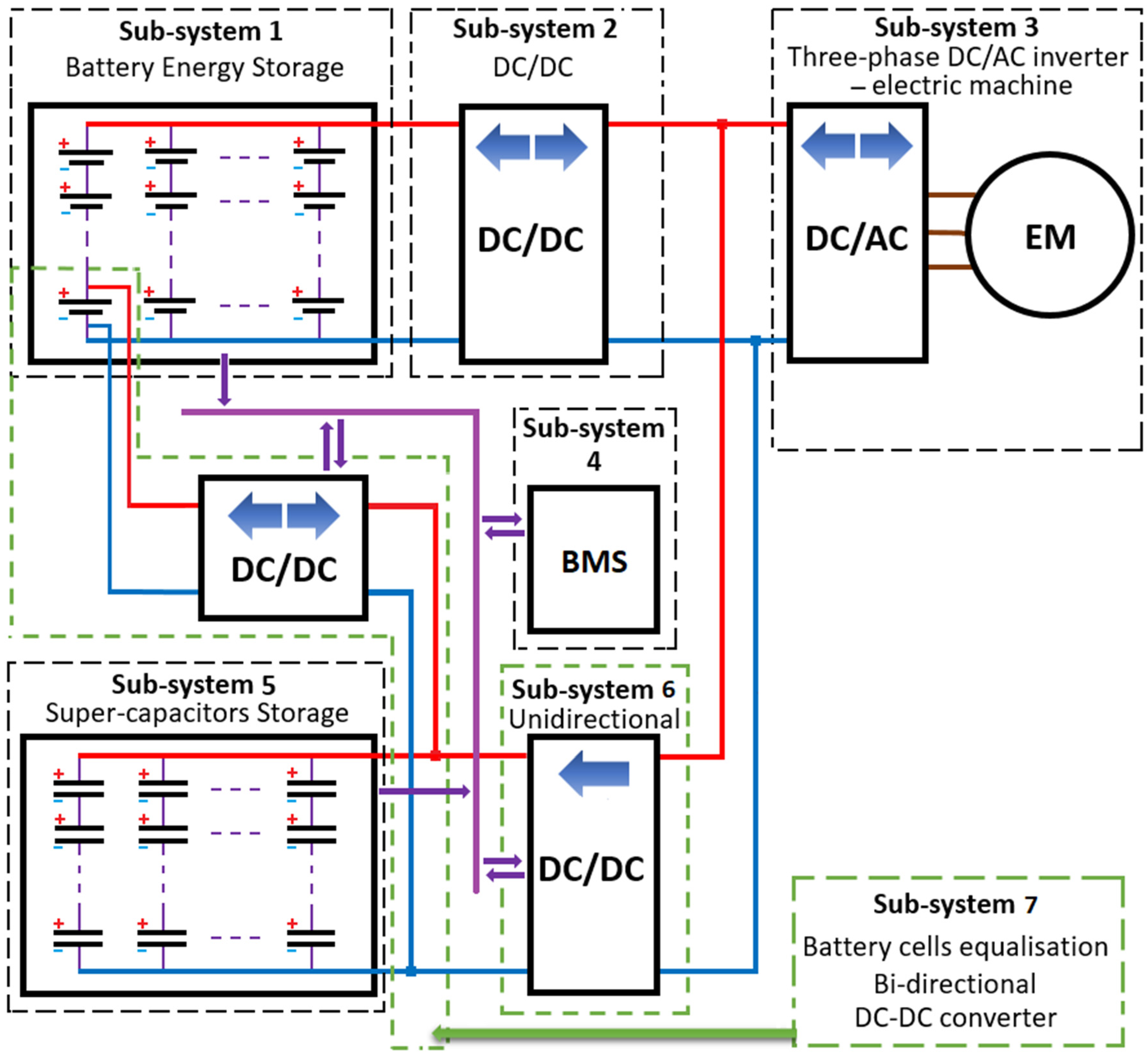
  • Sub-system 1: battery ES comprises cells connected in series strings that are then paralleled. In the models and design procedures that were further developed, only a cell is used as an element of charge equalisation.
  • Sub-system 2: bi-directional DC–DC converter transferring the energy between the battery and main inverter (out of scope).
  • Sub-system 3: traction inverter and motor (out of scope).
  • Sub-system 4: battery management system (BMS) controlling the equalisation process (out of scope).
  • Sub-system 5: SCES identical to the battery storage architecture. Based on analytical calculations, modelling, and simulations, the design procedure shows the recommended approach for the energy storage accommodation, giving the desired capacity and operational modes of charge and discharge.
  • Sub-system 6: unidirectional DC/DC converter used for SCES fast charge from regenerative break energy. The design procedure shows the applicability of the selected topology, considering the necessary high transformation ratio and power transfer.
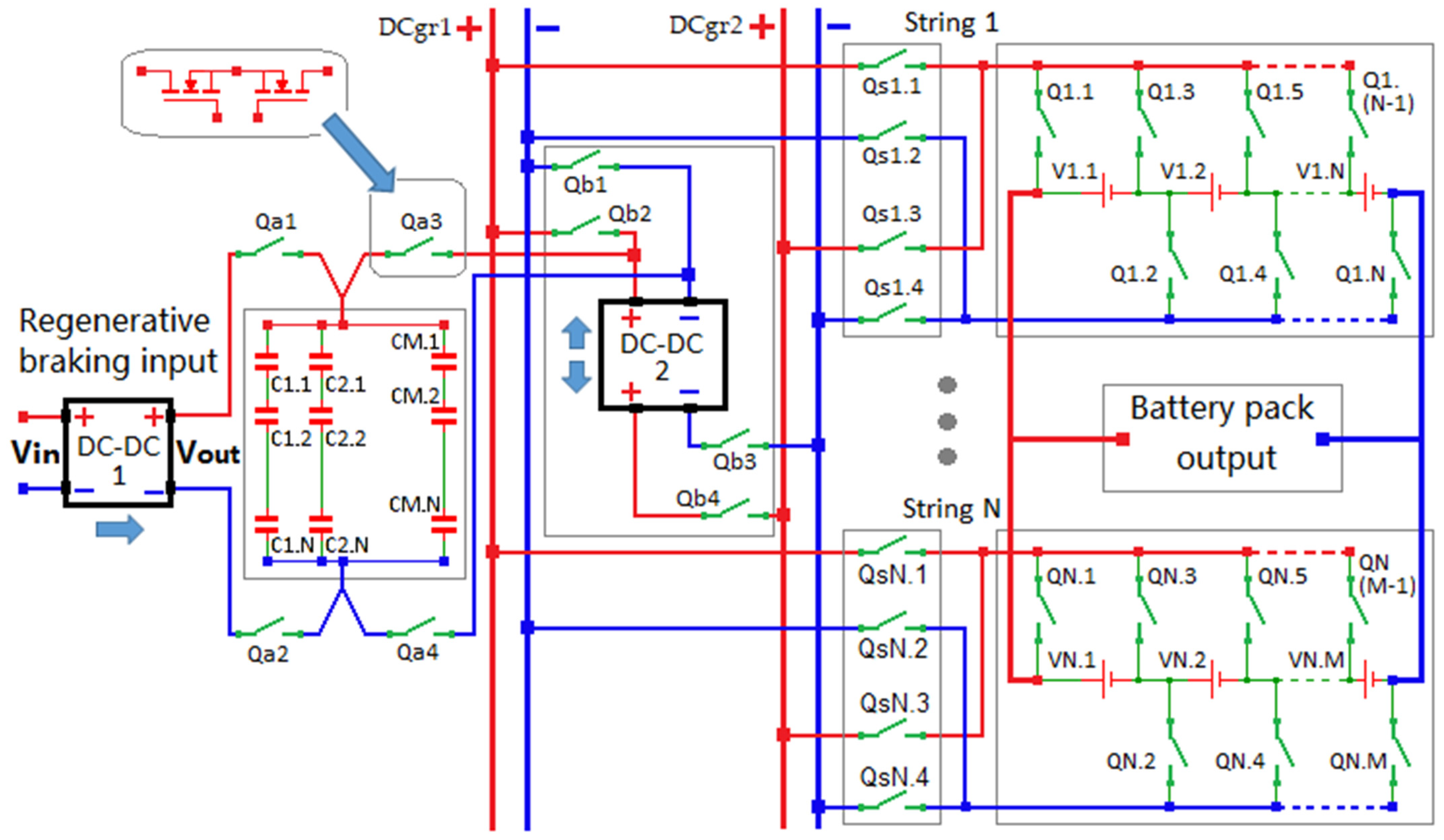
  • Sub-system 7: bi-directional DC/DC converter for battery cell equalisation. The design procedure shows the selected transformer-less topology applicability under the necessary modes of operation: battery cell charging/discharging from the SCES and battery cell equalisation by cell-to-cell energy transfer through the SCES.
The connection between the DC–DC converters, SCES tank, and the battery is shown in Figure 2. The structure is based on bi-directional MOSFET switches, the combination of each ensures a flexible system with connections between the SC tank and each battery cell through the converter DC–DC 2 (sub-system 7, Figure 1). Each battery string is connected to two DC Grids (DCgr1 and DCgr2) with two switches on the positive and negative side, which requires four input switches per each string (Qs1.1–Qs1.4, String 1). Two switches connect each battery cell to the positive and negative sides. The bi-directional energy transfer charging or discharging the battery cell is transferred respectively from or to the SCES. Energy cell-to-cell equalisation is possible between every two different strings, connecting DC–DC 2 between DCgr1 and DCgr2 with switches Qb1–Qb4. The same operation mode is unsupported between two cells in the same string. This mode must be achieved through the SCs, connecting the DC–DC 2 with the SC tank with two switches, Qa3 and Qa4. The SCs charging is given from DC–DC 1 (sub-system 6, Figure 1), taking energy from the regenerative braking (sub-system 3, Figure 1). This converter is connected to the SC tank with unidirectional switches Qa1, Qa2.
The number of switches of the string Q n . s t r is calculated from the number of cells per each string V c e l l s t r and the constant number of the input switches Q S N = 4 :
Q n . s t r = 2 × V c e l l s t r + 4
The total number of switches at the bi-directional DC–DC 2 converter ( Q b 1 Q b 4 ) is 4, as well as the total number of the SC tank ( Q a 1 Q a 4 ). The total number of switches for the entire system can be calculated from the number of the paralleled strings N s t r :
Q t o t a l = N s t r × Q n . s t r + 8
The switches’ ON/OFF operation is shown in Table 1, according to the systems’ modes of operation. To clarify the switching pattern, every operational mode is given for String 1 and String N, according to Figure 2.
The SCES design mainly focuses on estimating the stored energy necessary for the battery cell charging and the capacitors’ power loss estimation. This requires an analysis of the selected converter architecture, focused on the specific CC/CV charging modes of operation. The design procedure must define the necessary number of capacitors in series, strings in parallel (sub-system 4, Figure 1), and the total capacitance. The required energy for the battery cell charge is estimated as the constant power delivered over time, which must be delivered from the SC tank with no external source available. The energy stored in the SCES must be more than what is required for the charging process to be completed, compensating for the residual energy after each cycle. The precise amount, respectively, the integrated tank capacity and structure, is to be estimated analytically and depicted using simulation procedures. Considering the non-isolated bi-directional DC–DC converter, the maximum SCES voltage could be recommended in a range between 2 and 2.5 times the battery cells’ voltage. A value of 10 V is accepted, based on the nominal 3.7 V Li-ion battery cells voltage. The relatively small voltage difference allows a transformer-less bi-directional buck–boot DC–DC converter to be utilised, giving a simple structure and high efficiency.
The required capacitors’ energy W C is given with the integral of the power P C over the time t [3,4,6,7,12,19,20,29,30]:
W C = P C d t
The energy accumulated in a capacitor is given by the equation:
W C a p = 1 2 C V C a p 2
The transfer of the entire energy accumulated in the SCES physically requires the tank voltage to be discharged to 0 V. Such an operation would not sustain the charging process for several reasons: (a) the DC–DC converter cannot operate under its specific minimum voltage; therefore, the discharge to 0 V cannot maintain the power transfer; (b) the power discharge and energy curves follow the voltage curve proportionally, decreasing exponentially, which makes the power transfer ineffective; (c) with the voltage decrease, the discharge current must increase causing increased losses. Therefore, the SC tank discharge will cause a residual voltage V r e s . The ratio between the residual voltage and maximum tank voltage V m a x can be defined as the discharge radio D, expressed in percentages as follows [29,30]:
D = V r e s V m a x × 100
The maximum energy W m a x can be calculated for the entire pack using the maximum voltage V m a x :
W m a x = 1 2 C V m a x 2
The useable energy W u s e can be defined as a fraction of W m a x depending on the discharge coefficient ξ , specified over the discharge ratio as follows:
W u s e = W m a x × ξ
ξ = 1 D 2 100 2
The SCES charge and discharge basic equations [3,4,6,7,12,19,20,29,30] necessary for the simulation models are given in Table 2. The results of the simulations present the comparison between constant voltage (CV) and constant current (CC) illustrated, respectively, with block diagrams in Figure 3 and Figure 4. The charging DC–DC converter is a two-switch forward converter designed in the following part.
The simulations are conducted with a SCES with a structure suggested according to the above-presented considerations: SCs capacitance C s c = 100   F ; capacitors ESR R E S R = 35   m Ω ; capacitors nominal voltage V m a x   c a p s = 2.5   V ; maximum energy storage voltage V m a x = 10   V ; total energy storage capacitance C = 175   F , total storage tank ESR R E S R   t o t a l = 20   m Ω ; capacitors connected in series 5; capacitors’ strings connected in parallel 7.
Figure 5 shows the results for CV charging as follows: (A) the transient charging process continues for 17.5   s , e.g., five times the time constant T = 3.5   s with constant input voltage V i n = 10   V ; (B) the peak current at the beginning of the transient process is 499.86   A , and the average current is 100.72   A , which are considered unacceptable for the selected battery cells; (C) the peak capacitor loss is 44.64   W , and the average capacitor loss is 17.61   W ; (D) the peak power delivered to the energy storage is 1249.94   W , and the average power is 493.13 W ; (E) the peak energy is 8629.12   J , and the average accumulated energy is 6124   J .
Figure 6 shows the results for CC SC energy storage charging as follows: (A) the constant charging current is I C C h = 1   A , selected according to the maximum battery cells current and following the design of the DC–DC converter; (B) charging and tank voltages of 10.07   V , with a maximum capacitor voltage of 2.56   V reached in 21.8   s ; (C) the maximum capacitor loss at the end of the charge of 0.36   W and average capacitor loss of 0.06   W ; (D) the peak power delivered to the tank is 10.12   W , and the average power is 1.62   W , used as an input parameter for the equalisation DC–DC converter design; (E) the peak energy is 8967.48   J , and the average accumulated energy is 734.45   J .
The results from the CV and CC simulations in Figure 5 and Figure 6 show that CV SCs charge applies high energy stress over the charging power supply and the capacitors, caused by a high initial current and leading to a high capacitor loss. The CC charging mode shows superior energy parameters, giving lower capacitor loss and potentially lower stress over the charging DC–DC converter. As given in Figure 6, the energy transfer process and cell charge equalisation cannot be completed only in the CC operation. Therefore, CC/CV charging can be recommended in order to use the maximum energy storage capacity [29]. The results are depicted in Figure 7: (A) A block diagram showing the necessary current and voltage feedback, giving the CC/CV mode of operation; (B) the constant current of 1 A and the voltage reaching the constant voltage of 10 V; (C) peak and average capacitor loss, respectively, of 0.36   W and 0.04   W ; (D) the maximum power reaches 10.12   W with an average power of 1.1   W ; (E) the average accumulated energy is 5961.75   J .
The same CC/CV mode is used for SCES charging from regenerative break energy (converter DC–DC 1, Figure 2), as depicted in Figure 8: (A) CC of 100 A, estimated according to the regenerative braking parameters continues for 3 5   s ; (B) the SC tank nominal voltage reaches 10 V; (C) peak and average capacitor loss, respectively, of 29.27   W and 9.61   W ; (D) the maximum power of the converter is 819.61   W with an average power of 268.98   W ; (E) the average accumulated energy is 5661.75   J .

3. DC–DC Converters Analysis and Design

According to the above analysis, the two DC–DC converters (Figure 2) have different energy parameters, thus applying an individual set of requirements to their design. Converter DC–DC 1 converts high power, estimated at 1 kW. The high voltage input, estimated at 300–500 V to a low output voltage of 10 V, requires the topology to be transformer-based. Converter DC–DC 2 is bi-directional with power estimated at 10 W, converting the SCES voltage of 10 V to the battery cell voltage of 3.5 V and vice versa.

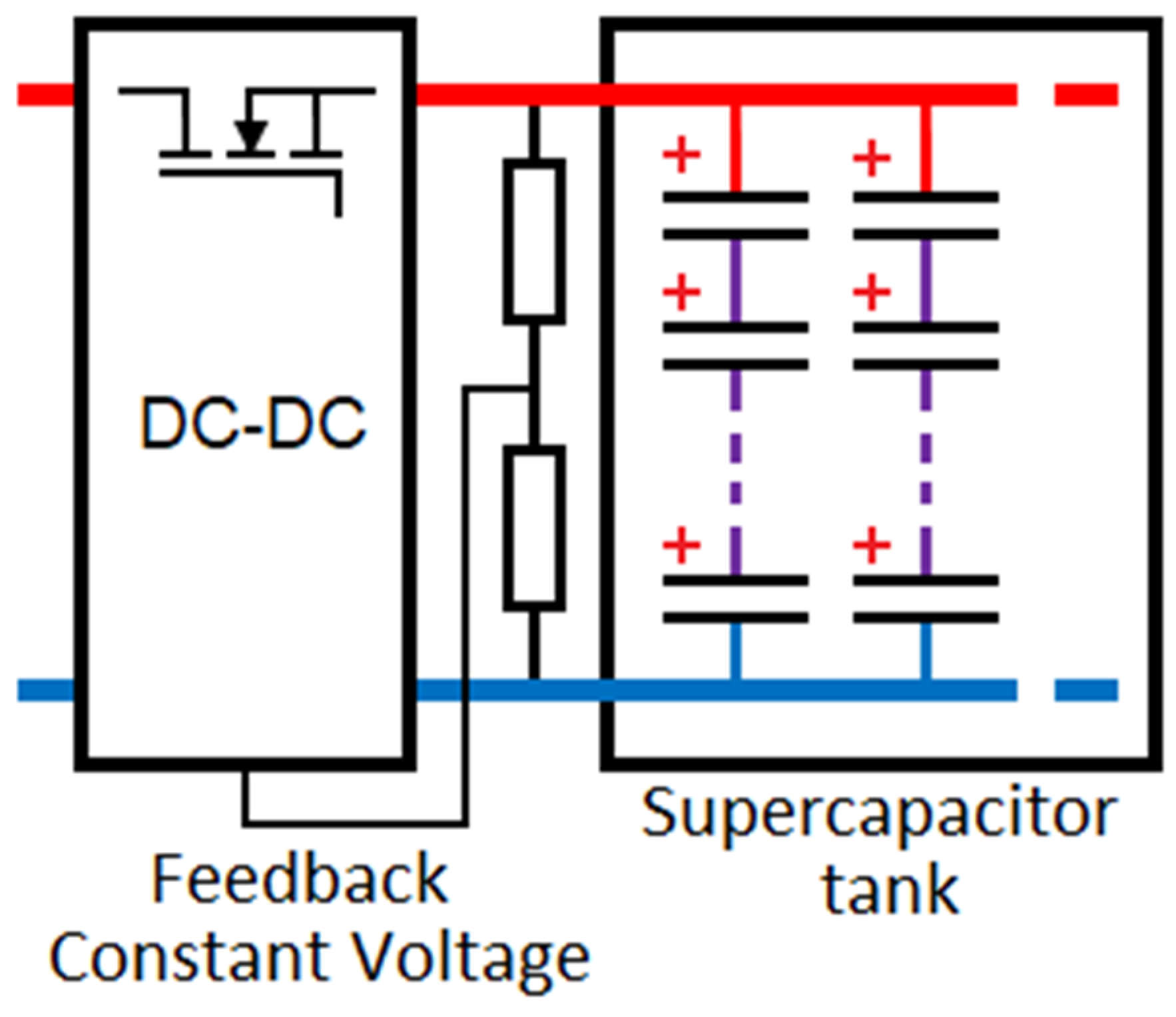
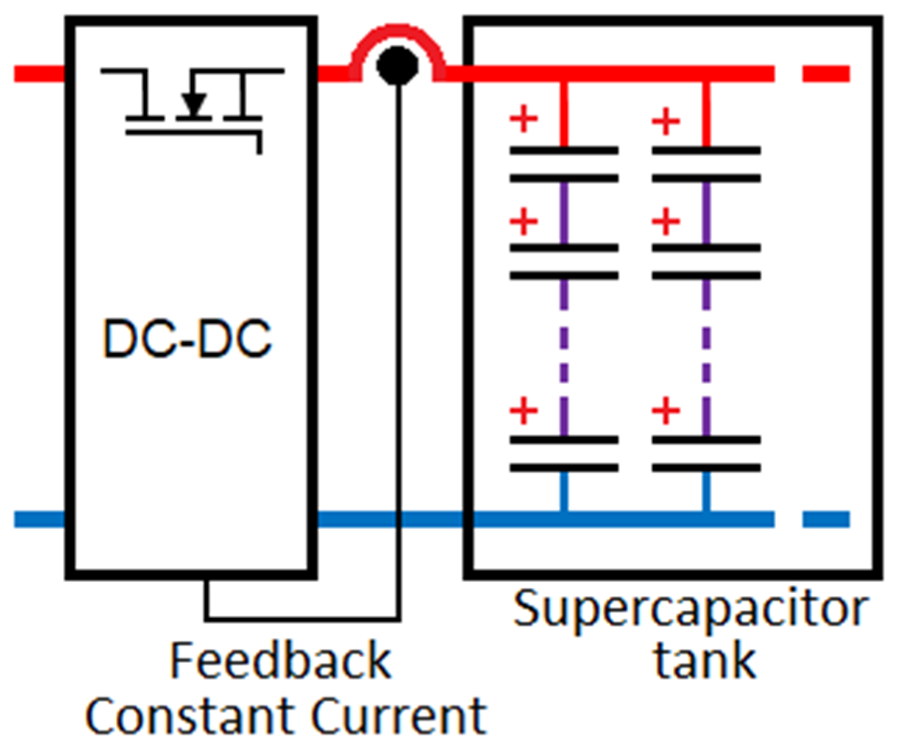
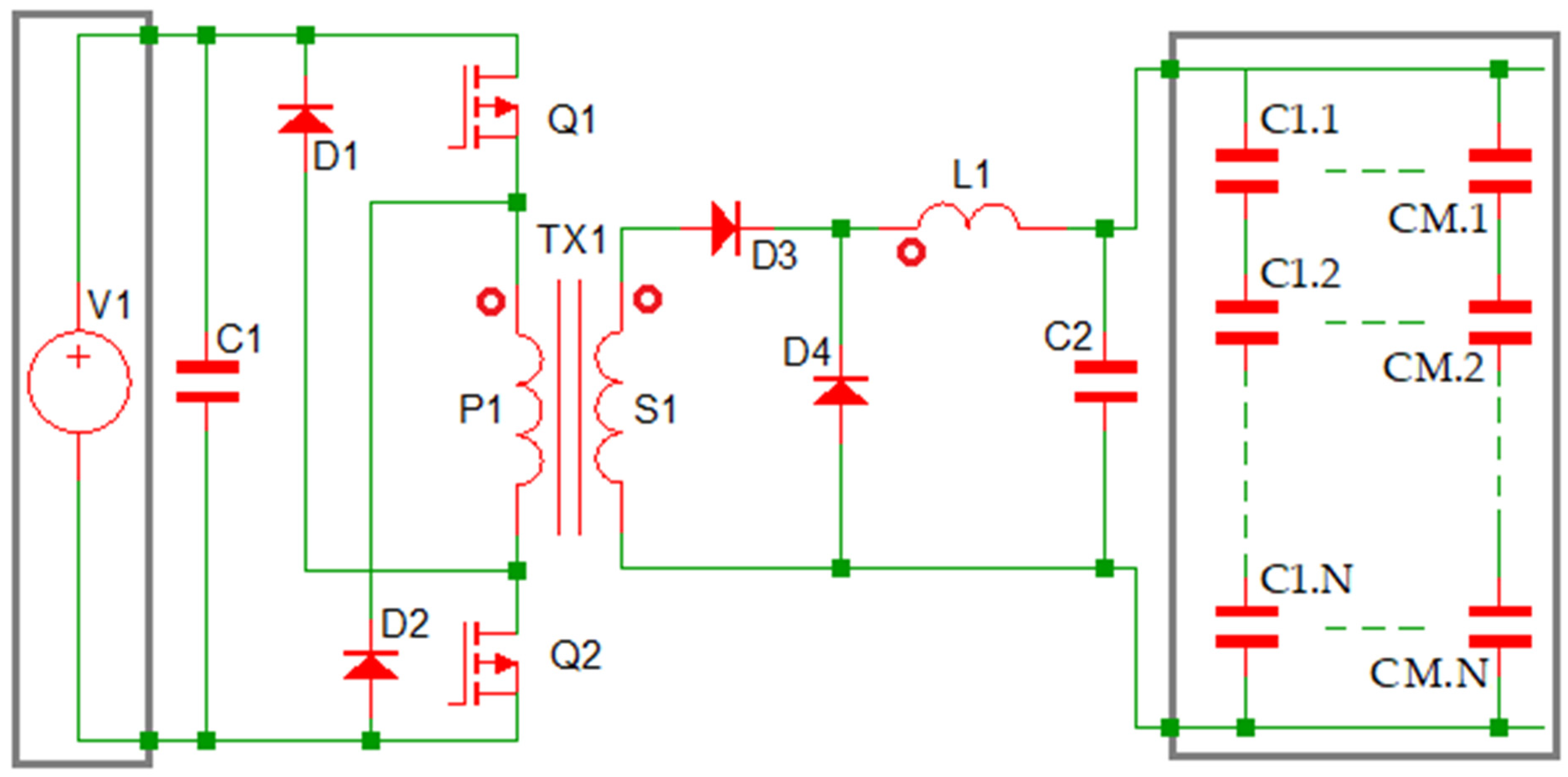
3.1. SCES DC/DC Charging Converter

The selected topology for the DC/DC charger is a two-switch forward converter which offers significant advantages in the designed battery cell charging sub-system: primary-to-secondary side transformer isolation; two switches in series on the primary side, giving additional potential for functional safety implementation in this topology; a simple structure and control system, providing a possibility for a budget-friendly solution; and relatively good, over 90%, expected efficiency for a hard-switching converter. Along with this, taking into account the specific energy requirements in the developed system, the inherent topology drawbacks can be mitigated: the secondary side inductor volume can be minimised; due to the relatively narrow secondary side voltage range and the significant primary to secondary side voltage difference, the duty cycle 50% limitation does not apply substantial design difficulties.
The converter is shown in Figure 9, where C1 is the input filter capacitor, Q1 and Q2 are primary side MOSFET switches, D1 and D2 are primary side demagnetisation diodes, TX1 is the high-frequency pulse transformer, diodes D3 and D4 form the secondary side rectifier and freewheeling diode, and the output filter is formed from the inductor L2 and capacitor C2. Following the suggested system architecture (Figure 1), the voltage source V1 represents sub-system 3, supplying the regenerative break energy, and the secondary side load is sub-system 5, e.g., the SCES under charge.
The transformer turns ratio can be calculated from the converter’s maximum output voltage [60,61]:
V o u t = η × V i n   m i n × D C m a x × N
where V o u t is the nominal output voltage; η is the estimated efficiency; V i n   m i n is the minimum operating input voltage; D C m a x is the maximum duty cycle; N is the turns ratio of the transformer.
The minimum voltage V i n   m i n must be matched with the SC minimum voltage, and, respectively, the residual pack voltage V r e s , giving the required discharge ratio, Equation (3). The converter output voltage must take into consideration the battery cell charging voltage, assumed as 4.2 V for Li-ion batteries, plus the expected voltage drops from the cell’s switches (Figure 2).
From the previous equation, the turns radio N and the duty cycle DC can be written as follows [60,61]:
N = V o u t η × V i n   m i n × D C m a x
D C m i n = V o u t η × V i n   m i n × N
The primary transformer inductance L m a g can be calculated assuming that the magnetising current is 10 % of the primary side current.
L m a g = V i n   m i n 0.1 × I p k p k D C m i x F S W
The output capacitor C o u t and the required equivalent series resistance R E S R can be calculated using the following equation:
C o u t I o u t 2 π f c × V o u t
R E S R 1 2 π f c × C o u t
where I o u t and V o u t are the output current and voltage ripples, and f c is the crossover frequency.
The estimated R E S R from the last equation must be minimised when the output capacitor is selected. The peak-to-peak output current ripple is calculated using the following equation [60,61]:
I L V r i p p l e R E S R
Having the output current ripple I L , the inductor value could be calculated using the following:
L = V o u t I L ( 1 D C m i n ) T S W
The secondary side peak current can be calculated using the equation
I sec   p k = I o u t + I L 2
The primary side current I pr   p k is calculated from the secondary side current I sec   p k , and the transformer turns ratio:
I pr   p k = I sec   p k × N r a t i o
The valley current will reach
I p _ v = I o u t I L 2 × N r a t i o
The primary side RMS current can be calculated using
I p r   r m s = D C m a x 1.1 × I p r   p k 2 1.1 × I p r   p k × I L × N + I L × N 2 3
Transistors’ conductive losses are given by the equation
P c o n d = I p r   r m s 2 × R D S ( o n )
The switching ON P s w   o n and OFF P s w   o f f losses are calculated from
P s w   o n = F S W 0 T o n I D S ( t ) × V D S ( t ) d t
P s w   o n = I p r   v a l × V i n   m a x × T 12 × F S W
P s w   o f f = I p r   p k × V i n   m a x × T 6 × F S W
where the time T is calculated from the gate drive charge Q G D and drive peak current I D R V   p k :
T = Q G D I D R   V p k
Primary side freewheeling diodes selection requires the primary side peak magnetisation current I m a g   p k and the rest time t r e s t to be calculated using
I m a g   p k = V i n   m i n L m a g × D C m a x F S W e w
t r e s t = I m a g   p k × L m a g V i n   m i n
The average current will be
I m a g   a v e r a g e = F S W I m a g   p k × t o n + t r e s t 2
The secondary side diodes ( D 3 and D 4 ) reverse voltage peak depends on the transformer turns ratio N r a t i o and maximum input voltage V i n   m a x :
V r e v   p k = N r a t i o × V i n   m a x k D
where k D is the diode derating factor. Considering the low-voltage secondary side, battery cell charge, it can be recommended that the range is k D = 0.6 0.7 .
The power dissipated from the rectifier D 3 is calculated from the forward voltage drop V f :
P D 3 = V f × I o u t × D C m a x
From the previous equation, the freewheeling diode D 4 dissipates:
P D 4 = V f × I o u t × 1 D C m a x
The converter parameters, calculated according to the presented methodology, are shown in Table 3.

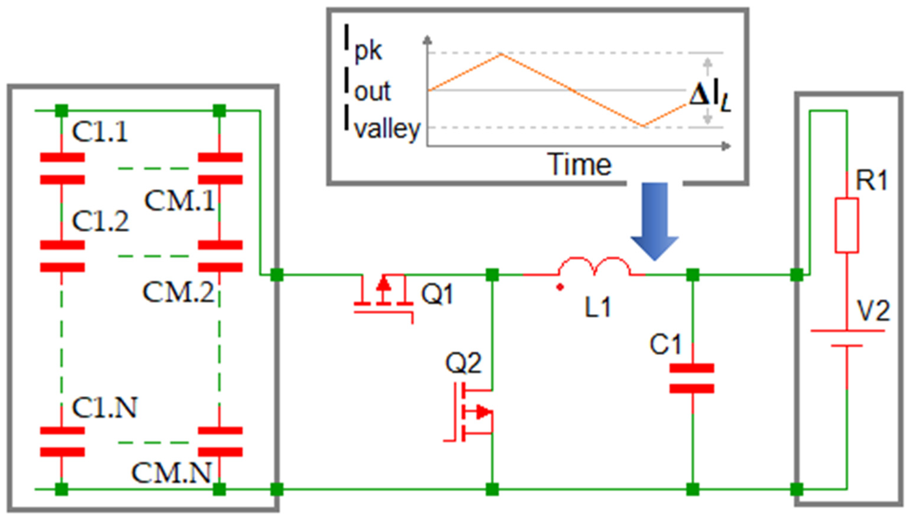
3.2. Bi-Directional Battery Cell Equalising DC/DC Converter Analysis and Design

The selected topology for the DC–DC 2 (Figure 2) is a transformer-less bi-directional buck–boost converter, shown in Figure 10. The converter comprises two MOSFET Q1 and Q2, inductor L1 and output capacitor C1. The SCES is connected on the primary side, and the battery cell (R1, V2) on the secondary side. The converter operates in buck mode charging the battery cell, or boost mode discharging the cell with overcharge.
High side Q1 and low side Q2 transistors loss (Figure 10), respectively, P o n Q 1 and P o n Q 2 are calculated using [62,63]
P o n Q 1 = I o u t 2 + I p k I v a l l e y 2 12 × R o n Q 1 × V o u t V i n
P o n Q 2 = I o u t 2 + I p k I v a l l e y 2 12 × R o n Q 2 × 1 V o u t V i n
where I p k is the peak ripple current value; I v a l l e y is the minimum valley ripple current value; I o u t is the average output current; V o u t and V i n are the output and input voltages; R o n Q 1 and R o n Q 2 are Q1 and Q2 ON resistances.
The inductor L1 value (Figure 10) can be determined from the above variables and the switching frequency F s w as follows:
L 1 = V i n V o u t F s w × I L × V o u t V i n
where the current ripple I L on the inductor is calculated using
I L = 2 × I p k I o u t = 2 × I p k I o u t
The switching losses of both transistors P S W Q 1 and P S W Q 2 can be calculated based on the transistors’ datasheet data for the rise t r i s e and fall t f a l l times and the switching frequency F S W as follows [62,63]:
P S W Q 1 = 1 2 × V i n × I o u t × t r i s e Q 1 + t f a l l Q 1 × F S W
P S W Q 2 = 1 2 × V D Q 2 × I o u t × t r i s e Q 2 + t f a l l Q 2 × F S W
where V D Q 2 is the Q2 body diode forward voltage drop.
The Q2 body diode reverse-recovery loss P D Q 2 is calculated using
P D Q 2 = 1 2 × V I N × I R R × t r r × F S W = Q r r × V I N × F S W
where I R R is the peak value of the body diode reverse recovery current; t r r is the body diode reverse recovery time; Q r r is the body diode reverse recovery charge.
The dead-time loss depends on the rise t r i s e D T and fall t f a l l D T dead-times.
P D T = V D Q 2 × I o u t × t r i s e D T + t f a l l D T × F S W
The gate loss can be calculated using the equation
P G a t e = Q g a t e Q 1 + Q g a t e Q 2 × V G S × F S W
where Q g a t e Q 1 and Q g a t e Q 2 are the gate charges of the transistors Q1 and Q2; V G S is the gate voltage.
The inductor loss P L D C R depends on the inductor resistance R D C R :
P L D C R = I o u t 2 + I p k I v a l l e y 2 12 × R D C R
The output capacitor loss is
P C 1 = I L 2 3 2 × R E S R C 1
The total converter loss is a sum of the above equations:
P t o t a l = P o n Q 1 + P o n Q 2 + P S W Q 1 + P S W Q 1 + P D Q 2 + P D T + P G a t e + P L D C R + P C 1
Output capacitor C1 (Figure 10) is calculated using the equation
C 1 = I o u t F s w × V p p × D C × 1 D C
where the DC is the duty cycle, and the V p p is the peak-to-peak voltage ripple.
The converter efficiency is estimated from the equation
η = V o u t × I o u t V o u t × I o u t + P t o t a l
The designed converter parameters are given in Table 4.

4. Battery Cell Equalisation Process Analysis

The battery cell equalisation is conducted in three operational modes: an undercharged cell is charged from the SC tank; an overcharged cell is discharged to the SC tank; cell-to-cell energy is transferred, respectively, from an overcharged to an undercharged cell in two different strings. As the first mode requires the SCES discharge, the impact of the same process on the tank energy parameters requires a more profound study.
Figure 11 shows the SCES discharge process from a model based on Equations (1)–(27). The negative current (A) is determined according to its direction from the tank to the battery cell. The tank voltage reaches the accepted minimum voltage for 178 s (B), which determines an area of operation (ON) and an area with residual voltage (OFF) in each DC–DC converter that does not operate. The exact process determines the residual energy after the process is completed.
Figure 12 shows a battery cell’s charge supported by the SCES as follows: (A) the block diagram of the SCES, DC–DC converter operating in buck mode, voltage and current sense networks, and the battery cell under charge; (B) SCES voltage, discharged from initial 10 V; (C) charging current to the battery cell flowing in a negative direction from the SCES to the battery cell; (D) constant power delivered to the battery cell; (E) energy accumulated in the SCES; (E) power loss in the SCs.
Figure 13A–D shows the SCES charge from a battery cell. This mode of operation supports the battery cell discharge due to overcharge. Considering the parameters of the cell equalisation buck–boost converter (DC–DC 2, Figure 2), it could be suggested that during normal operation, the SCES is always charged to an initial voltage. In this design, the minimum input voltage in the buck mode of operation is accepted at 6   V . Therefore, the result of the charging process between the minimum and maximum voltage is as follows: (A) constant charging current 1   A determines the maximum battery cell discharge current of 2   A (1) and maximum voltage over the SCES of 10   V (2); (B) capacitor’s peak power loss of 0.36   W giving an average power loss of 0.16   W ; (C) peak ( 10   W ) and average (4.57 W) power from the converter operating in boost mode; (D) peak ( 8829.89   J ) and average energy ( 6250.70   J ) transferred from the battery cell.
The same model is used to investigate the SCES charging process from the regenerative brake from the two-switch forward unidirectional converter (DC–DC 1, Figure 2). The results are depicted in Figure 13E–H as follows: (E) constant charging current 100   A (1), charging voltage (2), and capacitor’s tank voltage (3) change between 6   V and 10   V ; (F) capacitor’s peak power loss of 36.06   W giving an average power loss of 7.77   W ; (J) peak ( 1009.65   W ) and average ( 217.61   W ) power from the converter; (H) peak ( 8919.73   J ) and average energy ( 8185.88   J ) delivered from the charging converter.
The battery cell charging process, compensating for a voltage difference of 0.5 V during the battery pack operation, is depicted in Figure 14 as follows: (A) constant battery cell current (1) of 2 A, converters voltage (2), battery cell change from 2.5 V to 3 V; (B) converter primary side power (1) and converter secondary side power (2), giving an average amount of 2.76   W ; (C) peak ( 6751.65   J ) and average energy ( 6206.44   J ) accumulated from the battery cell. The average battery cell loss during equalisation is 0.1 W or 3.6%.
The overall system’s power loss depends on the converter’s loss, capacitor’s and battery cell’s loss, depicted with models and simulations, and the switch’s conductive loss. As a relatively high number of switches is required (Equations (1) and (2)), the number of active switches at each mode of operation and the conductive loss must be determined. As Table 5 shows, the SCES charge from the two-switch converter requires two unidirectional switches, the battery cell equalisation of eight bi-directional switches, the battery cell equalisation with energy distribution between two cells requires twelve bi-directional switches, and the battery cell discharge requires eight bi-directional switches. Considering all switches are connected in series, and only the conductive loss applies, the MOSFET transistors could be selected for a relatively low voltage but high current, giving a low drain-to-source resistance. Therefore, for Qa1 and Qa2, a transistor SiJA22DP is used with an ON resistance R O N = 0.0005   Ω . For all other switches, a pair of transistors IPD50P04P4-13 is used, each having an ON resistance of R O N = 0.009   Ω . According to the maximum expected currents in the designed system, the total power loss in the switches can be assumed as acceptable, taking into account that they are covered by the power coming from the regenerative braking.

5. Experimental Setup

To verify the suggested system for battery cell equalisation based on SCES, a simple model has been prototyped and tested. The model consists of the designed DC–DC converters in Part 2, and the designed SCES with 100   F SCs. Five SCs are connected in series in string and seven strings in parallel, giving a total storage capacitance of 175   F . The battery pack has been presented with a fraction of a real automotive battery, consisting of four Li-ion battery strings in parallel with seven cells each. With this, the installed resources were enough to emulate all operation modes in actual conditions.
The experimental results depict the system’s primary functions, presented with the experimentally recorded oscillograms in Figure 15, Figure 16, Figure 17 and Figure 18 as follows.
Figure 15 shows the SCES charging current and voltage from the DC–DC 1 converter (Figure 2). Probe 1 shows the current with the initial value of 100 A, and probe 2 shows the SCES voltage charge between 0 V and 10 V. The experiment supports the CV operation of charge. The experiment supports the simulations shown in Figure 5. The current is limited according to the converter parameters. The process continues for 12 s, simulating a charge from the regenerative brake of an electric vehicle. As shown, the peak current could be supported by the designed DC–DC converter, but the installed resource will not be fully used. Hence, the charging time exceeds the expected regenerative brake time, compromising the system’s efficiency.
Figure 16 shows the SCES charging with CC operation. The experiment supports the simulation results shown in Figure 6. The constant current is fixed at 100 A, which continues for 4.6 s. For this time, the voltage rises from 0 to the maximum of 10 V, after which the system operates with CV. The installed converter’s maximum power is better used, and the charging time complies with the expected regenerative brake time.
Both experiments support the validity of the designed two-switch converter (point 3.1, Figure 9) for SCES charge from the regenerative brake.
Figure 17 shows the DC–DC 2 converter (Figure 2) in the buck mode of operation during a battery cell equalisation. Probe 1 is the current over the inductor L1, probe 2 is the voltage over the MOSFET Q1 (Figure 10), and probe 3 is the PWM signal to the Q1 gate. The voltage peaks over the transistor’s drain-to-source are acceptable but could be limited with snubber capacitors. The calculated inductor of 150   μ H is selected with a saturation current of 2 A, i.e., double the nominal current. This inductor could be further increased in order for the current ripples to be reduced.
Figure 18 shows the output DC–DC 2 voltage (probe 1) and current (probe 2) to the battery cell during the charging process. Probes 3 and 4 are the controlled PWM impulses to both Q1 and Q2 transistors at a switching frequency of 100   k H z .
Both experiments show the validity of the designed buck–boost converter in point 3.2, Figure 10.
Figure 19 shows the SC discharge process (time T1) and SC charge process (time T2) due to battery equalisation. This experiment depicts the energy transferred to a battery cell for T1 = 50 s when the same is undercharged and the energy transferred from the battery to the SC tank for T2 = 10 s when the battery cell is overcharged. Probe 1 depicts the SCs tank voltage between the maximum 10 V and minimum 6 V, and probe 2 the current through the converter DC–DC 2 with a peak value of 1 A.
The final experiment depicts the functionality of the entire system. The obtained results comply with and complete the results obtained in [34,36,37].
The conducted experimental verification confirms the working capacity of the designed system, the possibility of completing all modes of operation, the stable operation of the designed converters and SCES, and the lack of oscillations and thermal losses in the converters and bi-directional switches.

6. Conclusions

In this paper, a battery cell equalisation system for automotive applications based on SCES has been analysed, designed, prototyped, and experimentally tested. The suggested system, presented in Figure 1 and Figure 2, shows stable work, equalising the battery cells SoC with the ability to allocate each cell from the battery pack in order for the charge or discharge processes to be completed with only one DC–DC converter (DC–DC 2, Figure 2). For this purpose, bi-directional switches were implemented, operating with acceptable power loss (Table 5). A buck–boost topology with 1 A 12 V/5 V parameters was used for the battery cells’ equalisation.
The system benefits from an additional SC tank used as ES to accumulate energy from the regenerative brake. For this design, the SC tank consists of a total capacitance of 175 F, a maximum voltage of 10 V, and an accumulated energy of 8750   J . The installed resource is enough for battery cell equalisation, according to the suggested topology in Figure 1 and Figure 2.
The charging process is supported by a unidirectional DC–DC converter (DC–DC 1, Figure 2), converting the regenerative brake energy to the SC tank charge. It has been revealed that the converter’s main parameters of 100 A nominal current, 300–500 V input voltage, and low 12 V output vulgate can be recommended for various automotive applications.
For the future development, design, and integration of the suggested system in automotive applications, the following recommendations could be systemised:
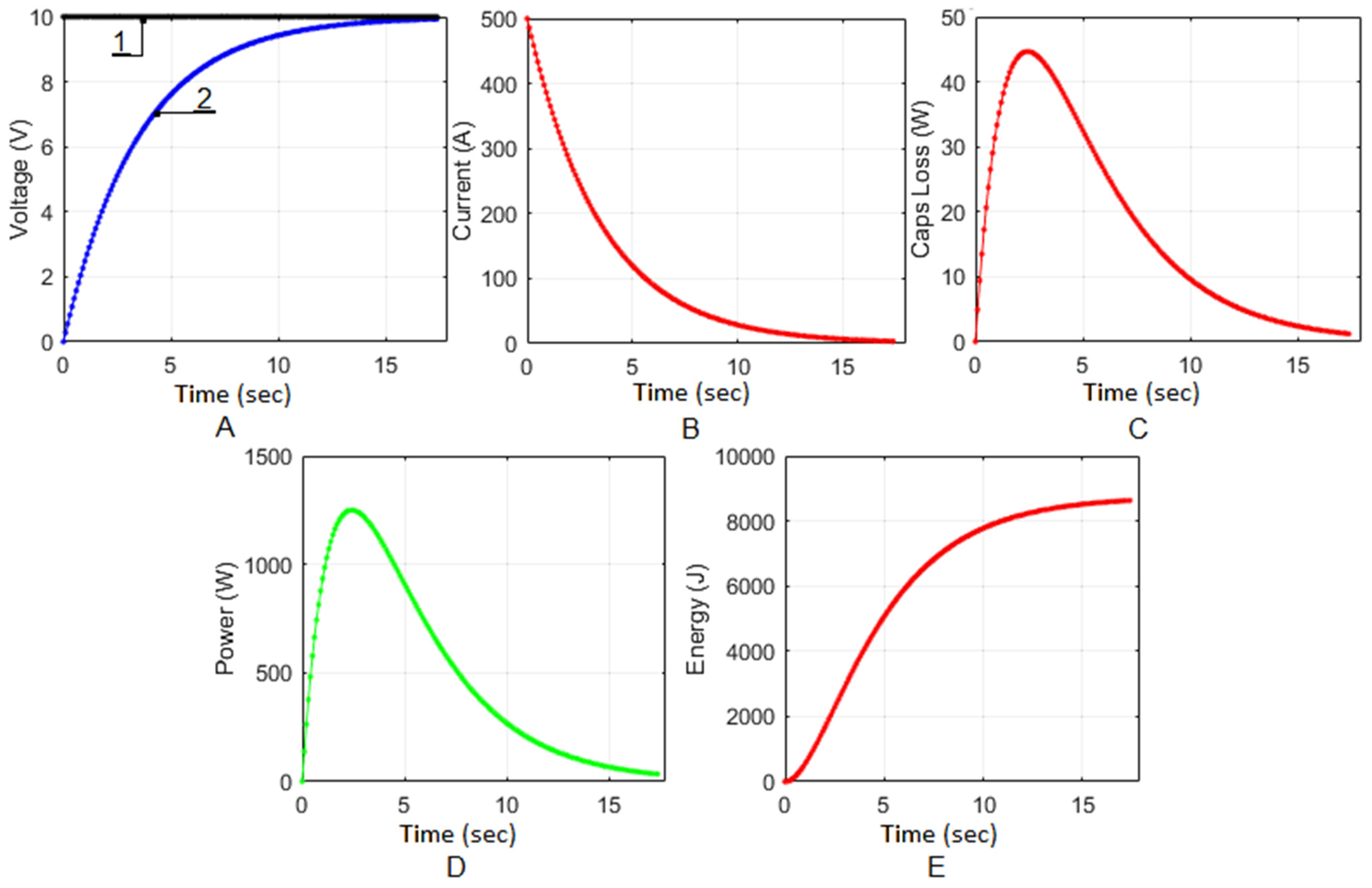
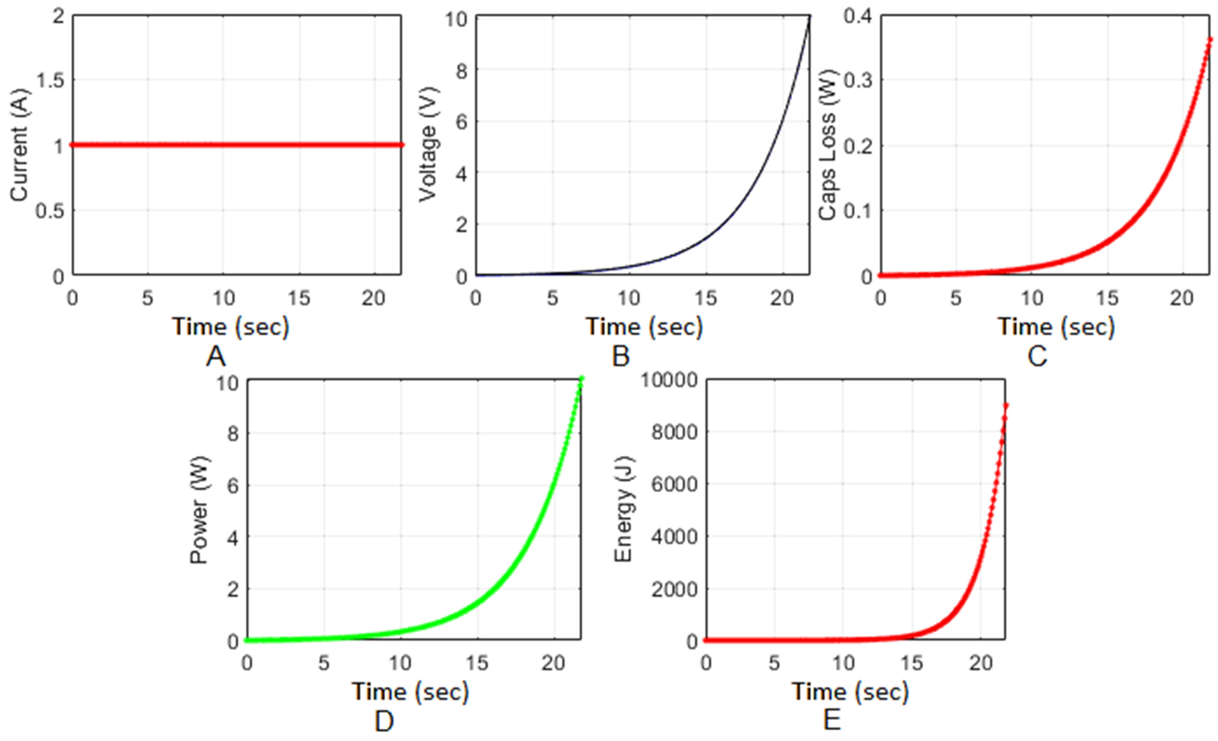
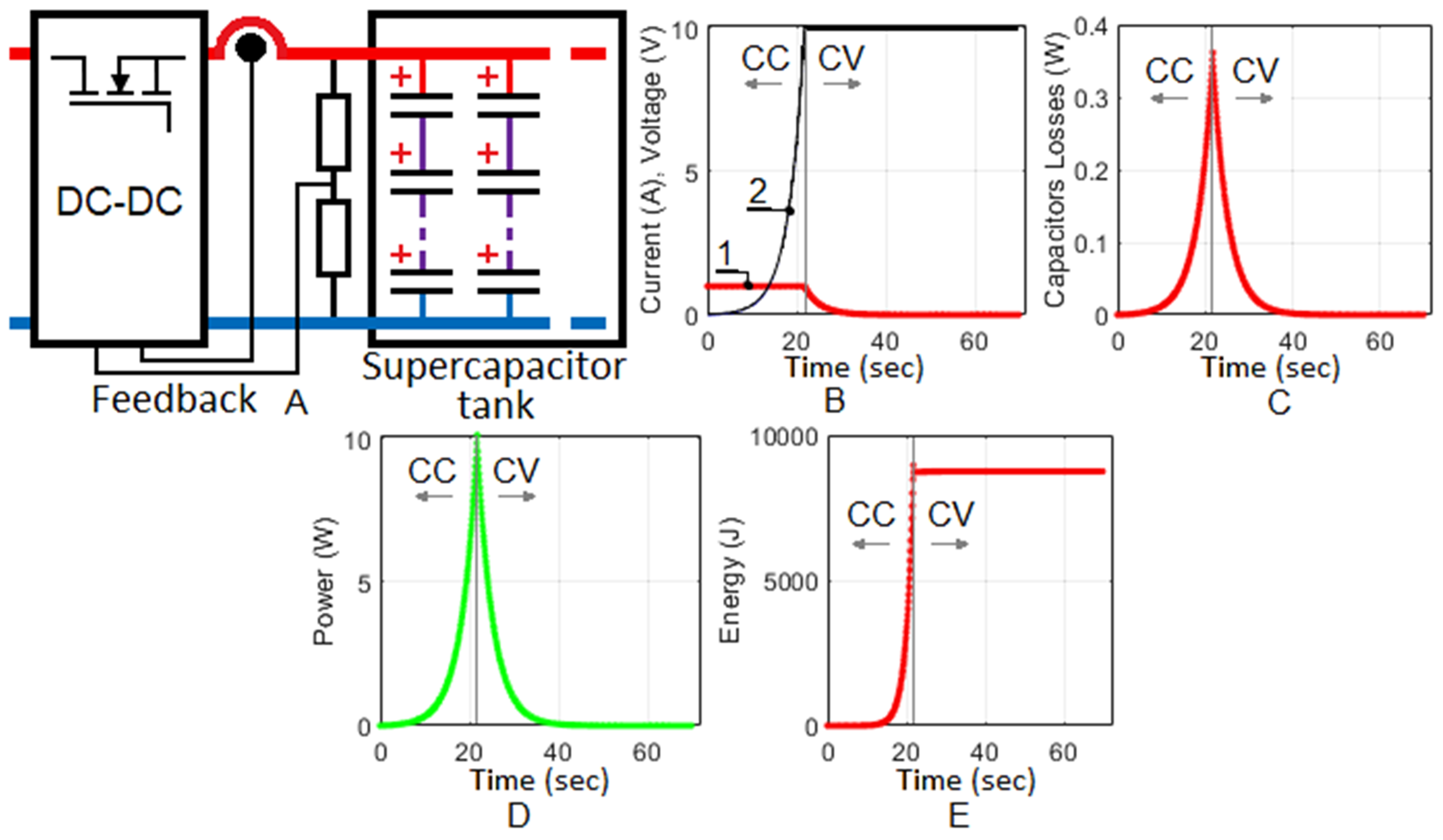
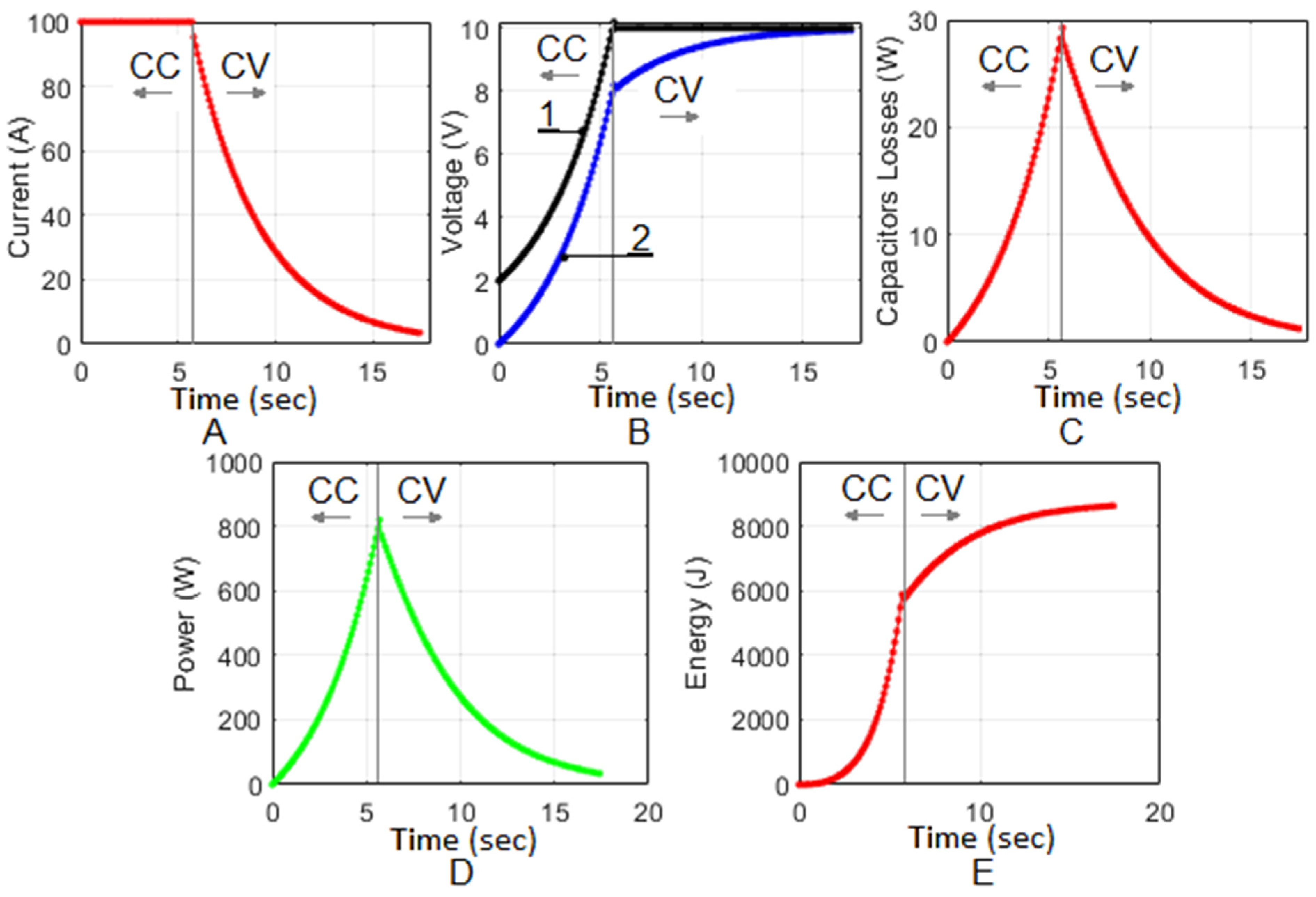
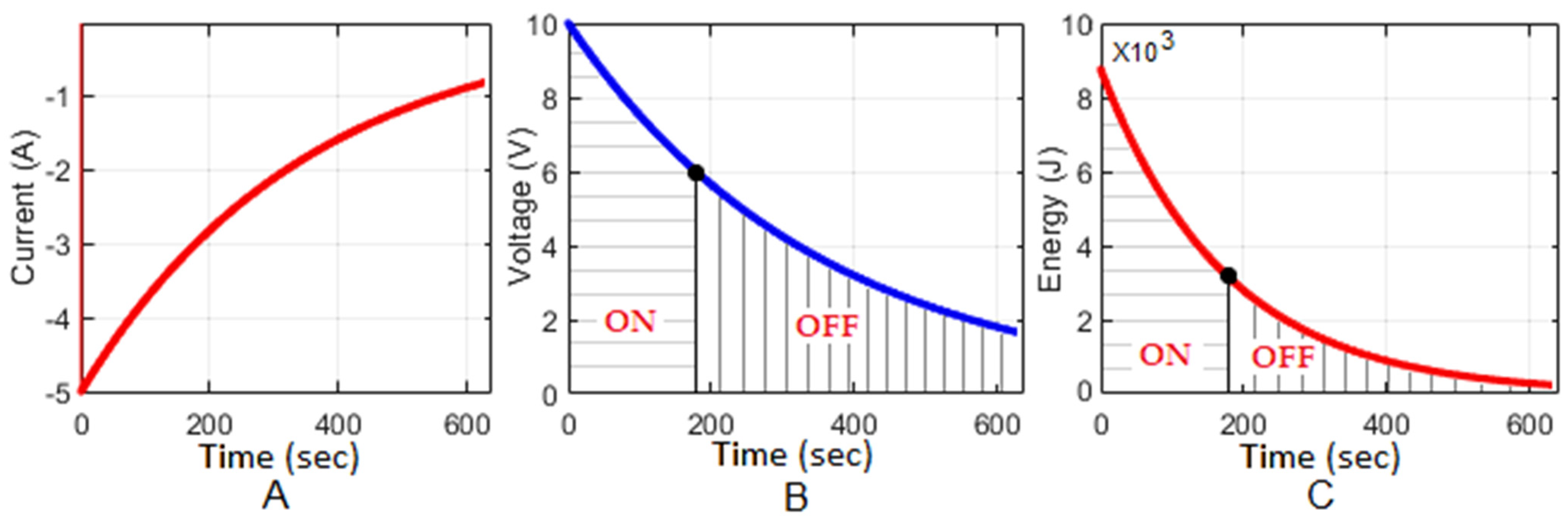
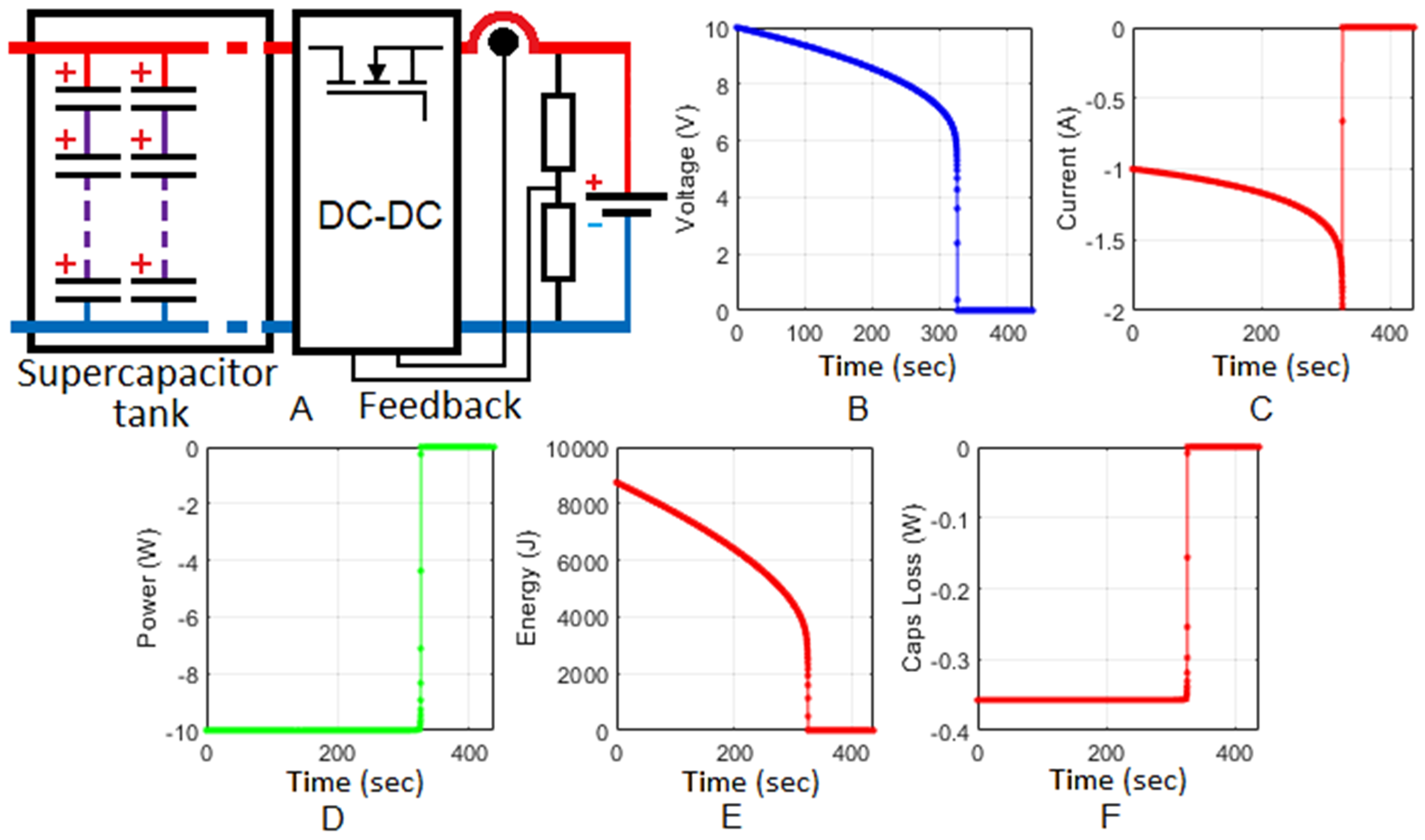
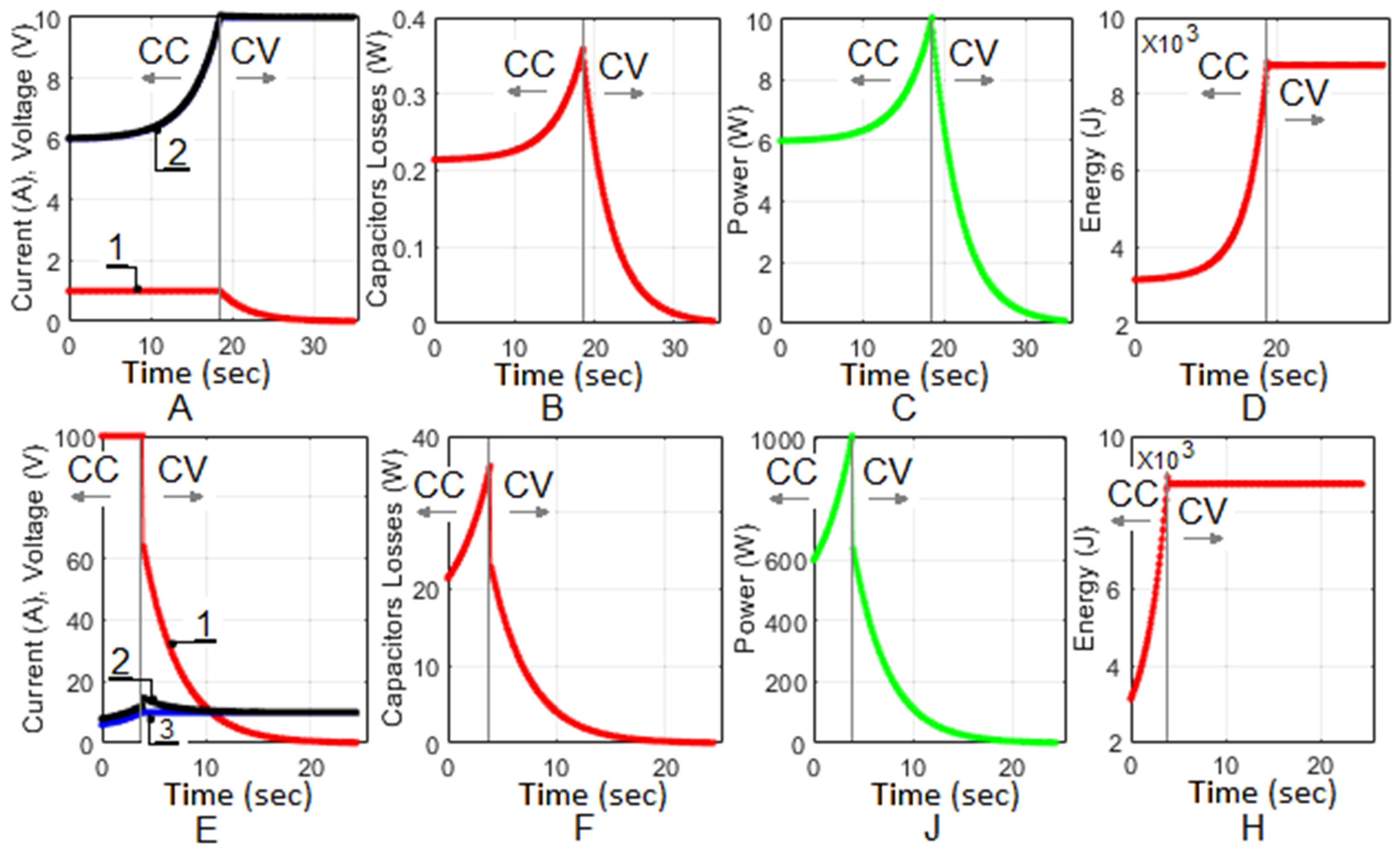
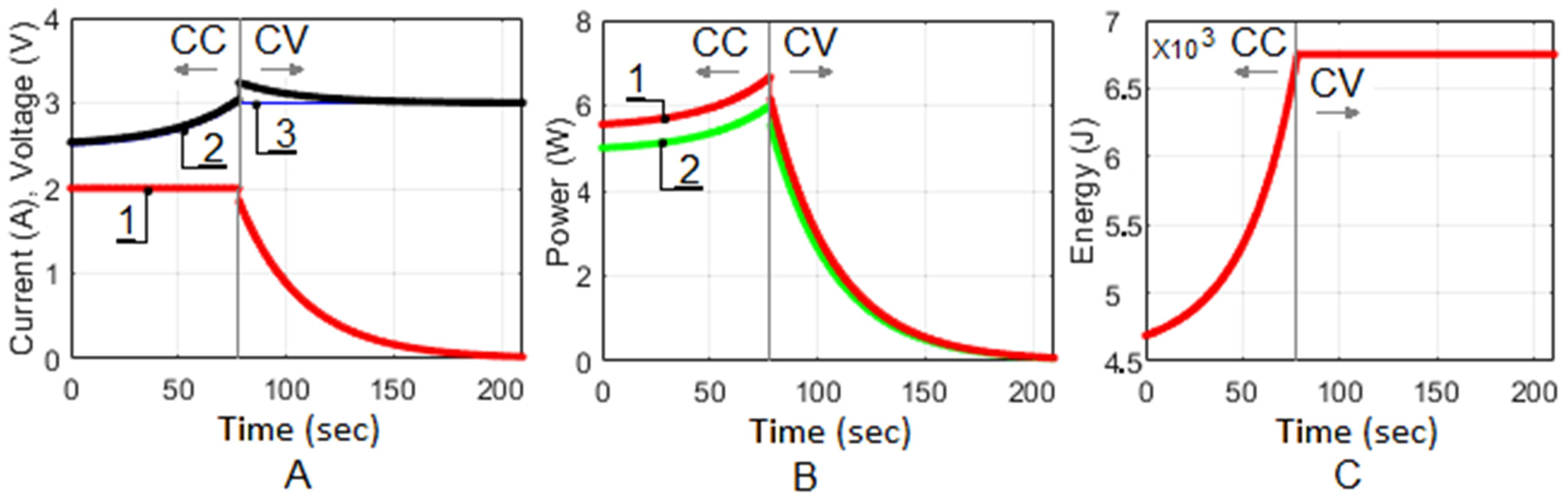
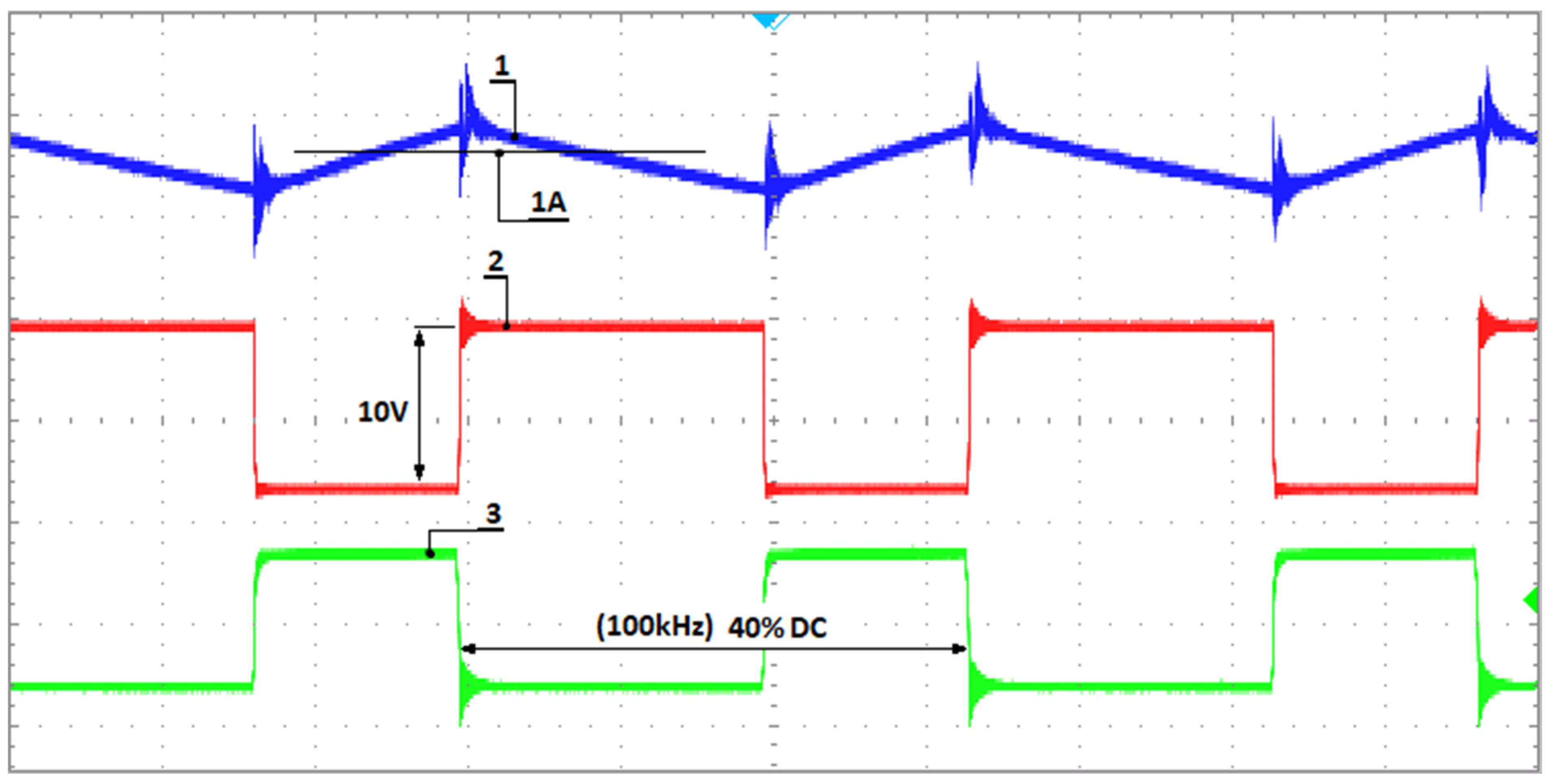
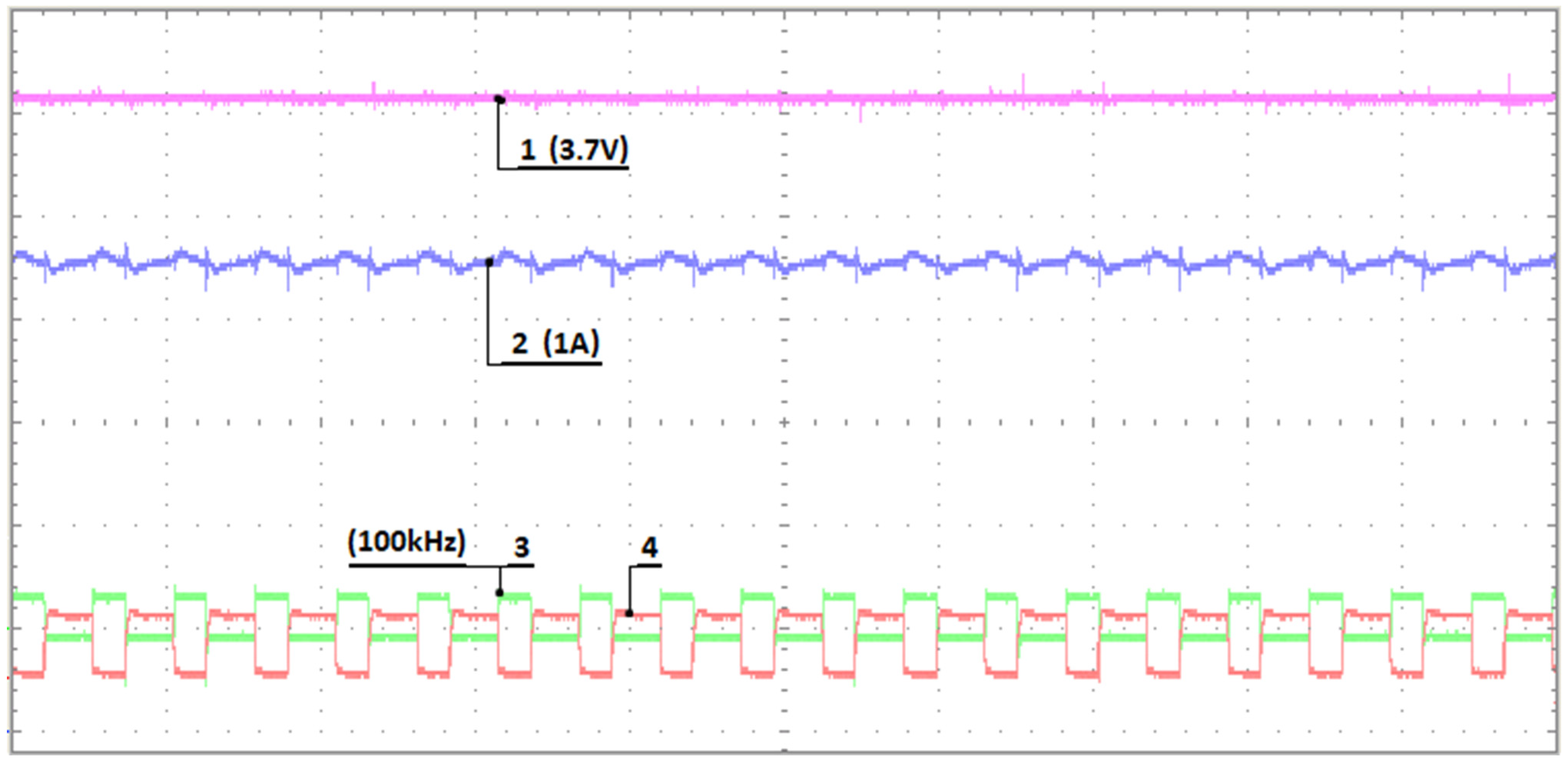
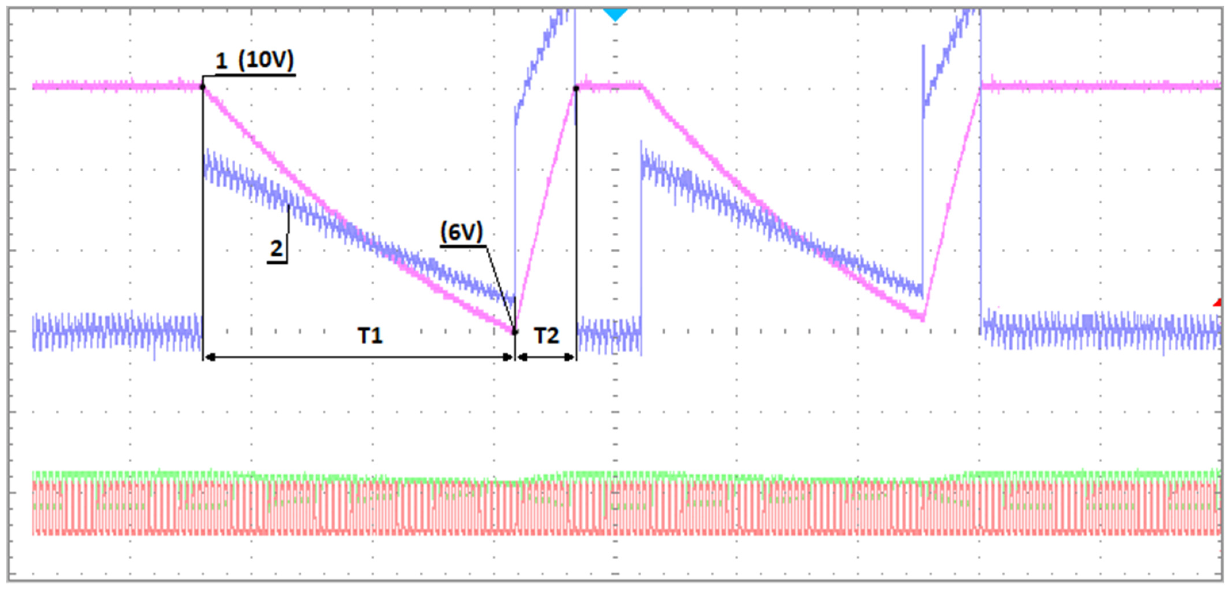
  • The design of the SCES could be supported with models based on the presented apparatus (Table 2), which gives a reasonable estimation of the transient processes of SCs charge/discharge and power loss (Figure 5, Figure 6, Figure 7 and Figure 8). Also, the models can be used to depict the battery cell equalisation process and power transfer, as shown in Figure 11, Figure 12, Figure 13 and Figure 14. The obtained results comply with the results published in [10,24].
  • The charging of the SCES could be based on CC operation as presented in Figure 6, Figure 7 and Figure 8. Charging the SCs with CV in this application should be avoided. The result complies with and completes the results in [29,30].
  • To minimise the power loss in the bi-directional switches, the transistors could be oversized on current, which minimises the D C o n resistance. Regarding targeted resistance, the range of R O N = 1   m Ω 500   μ Ω can be recommended.
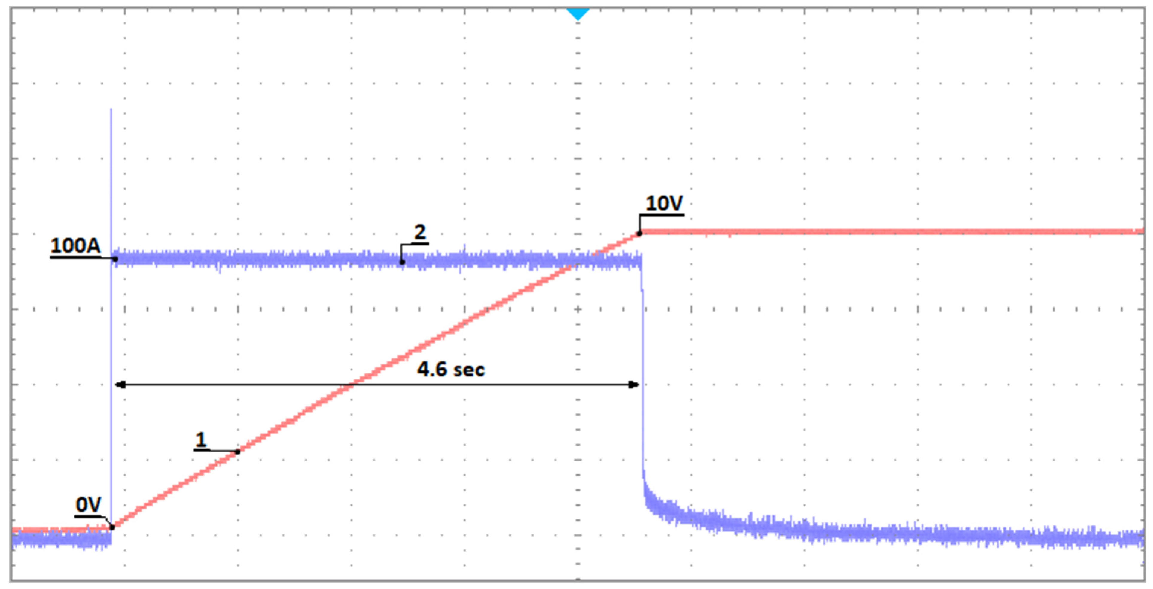
  • A buck–boost transformer-less converter (Figure 10) is a good choice for the battery cell equalisation converter as it has a simple structure and offers high power density. To accommodate this converter easily, the SCES could be selected with a nominal voltage of 2–3 times the charge voltage of the battery cells. For the SCES charge, the two-switch forward converter (Figure 9) is a good choice, as can be concluded from its experimental verification. The results comply with and complete the results published in [49,50,51,52,53,54,55].
  • The two-switch converter topology is a good choice for the SCES charge from the regenerative brake, operating stably in the entire input voltage range. The results comply with and complete the results published in [59,60,61].

Author Contributions

Validation, B.D.; Investigation, B.D. and S.K.; Writing—original draft, B.D.; Writing—review & editing, S.K. All authors have read and agreed to the published version of the manuscript.

Funding

This research received no external funding.

Data Availability Statement

No supporting data available.

Conflicts of Interest

The authors declare no conflict of interest.

References

  1. Liu, F.; Dai, J. Equalization circuit topologies of lithium battery strings: A brief review. J. Phys. Conf. Ser. 2020, 1633, 012141. [Google Scholar] [CrossRef]
  2. Liu, X.; Wan, Z.; He, Y.; Zheng, X.; Zeng, G.; Zhang, J. A Unified Control Strategy for Inductor-Based Active Battery Equalisation Schemes. Energies 2018, 11, 405. [Google Scholar] [CrossRef] [Green Version]
  3. Lei, X.; He, J.; Fan, L.; Wang, G. Active Equalization Strategy for Lithium-Ion Battery Packs Based on Multilayer Dual Interleaved Inductor Circuits in Electric Vehicles. J. Adv. Transp. 2022, 2022, 8653547. [Google Scholar] [CrossRef]
  4. Liao, L.; Chen, H.; Sun, S.; Li, H.; Jiang, J.; Wu, T. Research on Equalization Strategy Based on Credibility Factor Inference for Lithium-Ion Battery Packs. IEEE Access 2022, 10, 107980–107992. [Google Scholar] [CrossRef]
  5. Daowd, M.; Antoine, M.; Omar, N.; Van den Bossche, P.; Van Mierlo, J. Single Switched Capacitor Battery Balancing System Enhancements. Energies 2013, 6, 2149–2174. [Google Scholar] [CrossRef] [Green Version]
  6. Arasaratnam, I.; Tjong, J.; Habibi, S. Switched-Capacitor Cell Balancing: A Fresh Perspective; SAE Technical Paper 2014-01-1846; SAE: Warrendale, PA, USA, 2014. [Google Scholar] [CrossRef]
  7. Wang, X.; Cheng, K.; Fong, Y. Series-Parallel Switched-Capacitor Balancing Circuit for Hybrid Source Package. IEEE Access 2018, 6, 34254–34261. [Google Scholar] [CrossRef]
  8. Shimizu, T.; Koizumi, H. Modularised chain structure of switched capacitor for cell voltage equaliser with T-connected bi-directional switch. In Proceedings of the 2016 IEEE International Symposium on Circuits and Systems (ISCAS), Montreal, QC, Canada, 22–25 May 2016; pp. 1194–1197. [Google Scholar] [CrossRef]
  9. Takeda, Y.; Koizumi, H. Modularized double-tiered switched capacitor voltage equalizer. In Proceedings of the IECON 2017—43rd Annual Conference of the IEEE Industrial Electronics Society, Beijing, China, 29 October–1 November 2017; pp. 2782–2787. [Google Scholar] [CrossRef]
  10. Wasim, M.S.; Habib, S.; Amjad, M.; Bhatti, A.R.; Ahmed, E.M.; Qureshi, M.A. Battery-Ultracapacitor Hybrid Energy Storage System to Increase Battery Life Under Pulse Loads. IEEE Access 2022, 10, 62173–62182. [Google Scholar] [CrossRef]
  11. Podder, A.K.; Chakraborty, O.; Islam, S.; Kumar, N.M.; Alhelou, H.H. Control Strategies of Different Hybrid Energy Storage Systems for Electric Vehicles Applications. IEEE Access 2021, 9, 51865–51895. [Google Scholar] [CrossRef]
  12. He, D.; Luo, J.; Lin, D.; Yu, S. Flexible predictive power-split control for battery-supercapacitor systems of electric vehicles using IVHS. J. Syst. Eng. Electron. 2023, 34, 224–235. [Google Scholar] [CrossRef]
  13. Lu, X.; Chen, Y.; Fu, M.; Wang, H. Multi-Objective Optimization-Based Real-Time Control Strategy for Battery/Ultracapacitor Hybrid Energy Management Systems. IEEE Access 2019, 7, 11640–11650. [Google Scholar] [CrossRef]
  14. Panhwar, I.H.; Ahmed, K.; Seyedmahmoudian, M.; Stojcevski, A.; Horan, B.; Mekhilef, S.; Aslam, A.; Asghar, M. Mitigating Power Fluctuations for Energy Storage in Wind Energy Conversion System Using Supercapacitors. IEEE Access 2020, 8, 189747–189760. [Google Scholar] [CrossRef]
  15. Roy, P.; He, J.; Liao, Y. Cost Minimization of Battery-Supercapacitor Hybrid Energy Storage for Hourly Dispatching Wind-Solar Hybrid Power System. IEEE Access 2020, 8, 210099–210115. [Google Scholar] [CrossRef]
  16. Cabrane, Z.; Lee, S.H. Control and Management of Railway System Connected to Microgrid Stations. IEEE Access 2022, 10, 40445–40455. [Google Scholar] [CrossRef]
  17. Sayed, K.; Abdel-Khalek, S.; Zakaly, H.M.H.; Aref, M. Energy Management and Control in Multiple Storage Energy Units (Battery–Supercapacitor) of Fuel Cell Electric Vehicles. Materials 2022, 15, 8932. [Google Scholar] [CrossRef]
  18. Torres, J.; Moreno-Torres, P.; Navarro, G.; Blanco, M.; Lafoz, M. Fast Energy Storage Systems Comparison in Terms of Energy Efficiency for a Specific Application. IEEE Access 2018, 6, 40656–40672. [Google Scholar] [CrossRef]
  19. Yaqoob, S.J.; Ferahtia, S.; Obed, A.A.; Rezk, H.; Alwan, N.T.; Zawbaa, H.M.; Kamel, S. Efficient Flatness Based Energy Management Strategy for Hybrid Supercapacitor/Lithium-ion Battery Power System. IEEE Access 2022, 10, 132153–132163. [Google Scholar] [CrossRef]
  20. Pai, F.-S.; Huang, S.-J.; Ku, C.-W.; Chen, Y.-R.; Huang, B.-G.; Lin, Y.-C. Voltage equalization of lithium iron phosphate batteries cooperating with supercapacitors. In Proceedings of the 2014 IEEE International Symposium on Circuits and Systems (ISCAS), Melbourne, VIC, Australia, 1–5 June 2014; pp. 618–621. [Google Scholar] [CrossRef]
  21. Pour, G.B.; Ashourifar, H.; Aval, L.F.; Solaymani, S. CNTs-Supercapacitors: A Review of Electrode Nanocomposites Based on CNTs, Graphene, Metals, and Polymers. Symmetry 2023, 15, 1179. [Google Scholar] [CrossRef]
  22. Şahİn, M.; Blaabjerg, F.; Sangwongwanİch, A. Modelling of Supercapacitors Based on Simplified Equivalent Circuit. CPSS Trans. Power Electron. Appl. 2021, 6, 31–39. [Google Scholar] [CrossRef]
  23. Prasad, R.; Kothari, K.; Mehta, U. Flexible Fractional Supercapacitor Model Analyzed in Time Domain. IEEE Access 2019, 7, 122626–122633. [Google Scholar] [CrossRef]
  24. Xu, D.; Zhang, L.; Wang, B.; Ma, G. Modeling of Supercapacitor Behavior with an Improved Two-Branch Equivalent Circuit. IEEE Access 2019, 7, 26379–26390. [Google Scholar] [CrossRef]
  25. Krpan, M.; Kuzle, I.; Radovanovic, A.; Milanovic, J.V. Modelling of Supercapacitor Banks for Power System Dynamics Studies. IEEE Trans. Power Syst. 2021, 36, 3987–3996. [Google Scholar] [CrossRef]
  26. Li, Y.; Wang, S.; Zheng, M.; Liu, J. Thermal behavior analysis of stacked-type supercapacitors with different cell structures. CSEE J. Power Energy Syst. 2018, 4, 112–120. [Google Scholar] [CrossRef]
  27. Wu, M.; Wei, L.; Shen, Y. Electro-thermal coupling model of supercapacitor for online application. In Proceedings of the 2019 IEEE 4th International Future Energy Electronics Conference (IFEEC), Singapore, 25–28 November 2019. [Google Scholar]
  28. Liu, Y.; Zhang, C.; Jiang, J.; Jiang, Y.; Zhang, L.; Zhang, W. Capacity Estimation of Serial Lithium-ion Battery Pack Using Dynamic Time Warping Algorithm. IEEE Access 2019, 7, 174687–174698. [Google Scholar] [CrossRef]
  29. Rufer, A. Energy Storage Systems and Components; Taylor & Francis Group, LLC: Abingdon, UK, 2018; ISBN 978-1-138-08262-5. [Google Scholar]
  30. Kim, Y.; Chang, N. Design and Management of Energy-Efficient Hybrid Electrical Energy Storage Systems; Springer International Publishing: Cham, Switzerland, 2014; ISBN 978-3-319-07280-7. [Google Scholar] [CrossRef]
  31. Khalid, A.; Stevenson, A.; Sarwat, A.I. Overview of Technical Specifications for Grid-Connected Microgrid Battery Energy Storage Systems. IEEE Access 2021, 9, 163554–163593. [Google Scholar] [CrossRef]
  32. Hannan, M.A.; Hoque, M.D.M.; Hussain, A.; Yusof, Y.; Ker, A.P.J. State-of-the-Art and Energy Management System of Lithium-Ion Batteries in Electric Vehicle Applications: Issues and Recommendations. IEEE Access Spec. Sect. Adv. Energy Storage Technol. Appl. 2018, 6, 19362–19378. [Google Scholar] [CrossRef]
  33. Bolonne, S.R.A.; Chandima, D.P. Sizing an Energy System for Hybrid Li-Ion Battery-Supercapacitor RTG Cranes Based on State Machine Energy Controller. IEEE Access 2019, 7, 71209–71220. [Google Scholar] [CrossRef]
  34. Apribowo, C.H.B.; Adyatama, S.; Ramelan, A.; Adriyanto, F.; Nizam, M.; Sutrisno. Design and Implementation of Hybrid Equalization Battery Management System for Lithium-Ion Batteries. In Proceedings of the 2022 5th International Seminar on Research of Information Technology and Intelligent Systems (ISRITI), Yogyakarta, Indonesia, 8–9 December 2022; pp. 531–536. [Google Scholar] [CrossRef]
  35. Xia, X.; Zhao, X.; Zeng, H.; Zeng, X. A novel design of hybrid energy storage system for electric vehicles. Chin. J. Electr. Eng. 2018, 4, 45–51. [Google Scholar] [CrossRef]
  36. Zhang, H.; Wang, Y.; Qi, H.; Zhang, J. Active Battery Equalization Method Based on Redundant Battery for Electric Vehicles. IEEE Trans. Veh. Technol. 2019, 68, 7531–7543. [Google Scholar] [CrossRef]
  37. Gao, M.; Qu, J.; Lan, H.; Wu, Q.; Lin, H.; Dong, Z.; Zhang, W. An Active and Passive Hybrid Battery Equalization Strategy Used in Group and between Groups. Electronics 2020, 9, 1744. [Google Scholar] [CrossRef]
  38. Choy, W.J.; Costabeber, A.; Buticchi, G.; Trentin, A.; Walker, A.; Galea, M.; Paciura, K.; O’Brien, J.; Palmer, B. A Multiport Power Electronics Converter for Hybrid Traction Applications. IEEE Access 2021, 9, 99181–99192. [Google Scholar] [CrossRef]
  39. Zhan, H.; Wu, H.; Muhammad, M.; Lambert, S.; Pickert, V. Combining electric vehicle battery charging and battery cell equalisation in one circuit. IET Electr. Syst. Transp. 2021, 11, 377–390. [Google Scholar] [CrossRef]
  40. Wang, P.; Ren, P.; Lu, X.; Wang, W.; Xu, D. A Distributed State-of-Charge Balancing Control Scheme for Three-Port Output-Series Converters in DC Hybrid Energy Storage Systems. IEEE Access 2019, 7, 157173–157184. [Google Scholar] [CrossRef]
  41. Cavallo, A.; Russo, A.; Canciello, G. Control of Supercapacitors for smooth EMA Operations in Aeronautical Applications. In Proceedings of the 2019 American Control Conference (ACC), Philadelphia, PA, USA, 10–12 July 2019. [Google Scholar] [CrossRef]
  42. Russo, A.; Cavallo, A. Supercapacitor stability and control for More Electric Aircraft application. In Proceedings of the 2020 European Control Conference (ECC), Saint Petersburg, Russia, 12–15 May 2020. [Google Scholar]
  43. Cao, J.; Xia, B.; Zhou, J. An Active Equalization Method for Lithium-ion Batteries Based on Flyback Transformer and Variable Step Size Generalized Predictive Control. Energies 2021, 14, 207. [Google Scholar] [CrossRef]
  44. Dimitrov, B.; Krishna, M.; Cruden, A.; Sharkh, S.; Elkhateb, A. Analysis, Design and Experimental Validation of a Primary Side Current Sensing Flyback Converter for Use in a Battery Management System. Electronics 2018, 7, 43. [Google Scholar] [CrossRef] [Green Version]
  45. Karthikrajan, G.; Sindhu, M. Implementation and Analysis of Flyback converter for active charge equalization in Li-ion battery pack for EVs. In Proceedings of the 2020 International Conference on Power, Instrumentation, Control and Computing (PICC), Thrissur, India, 17–19 December 2020; pp. 1–5. [Google Scholar] [CrossRef]
  46. Sun, X.; Cai, C.; Nie, J.; Deng, Y.; Shu, Z. Battery Equalizer for Series-Connected Batteries Based on Half-Bridge LLC Topology. In Proceedings of the 2022 IEEE Applied Power Electronics Conference and Exposition (APEC), Houston, TX, USA, 20–24 March 2022; pp. 1898–1903. [Google Scholar] [CrossRef]
  47. Wei, Z.; Peng, F.; Wang, H. A String-to-Cell Battery Equalizer Based on Fixed-Frequency LCC Resonant Converter. In Proceedings of the 2020 IEEE Applied Power Electronics Conference and Exposition (APEC), New Orleans, LA, USA, 15–19 March 2020. [Google Scholar]
  48. Wu, Q.; Gao, M.; Lin, H. A mode-varying cell equaliser based on interleaved parallel multiple transformers. CSEE J. Power Energy Syst. 2023, 9, 802–823. [Google Scholar] [CrossRef]
  49. Song, S.; Xiao, F.; Peng, S.; Song, C.; Shao, Y. A High-Efficiency Bidirectional Active Balance for Electric Vehicle Battery Packs Based on Model Predictive Control. Energies 2018, 11, 3220. [Google Scholar] [CrossRef] [Green Version]
  50. Ji, W.; Ran, F.; Ji, Y.; Lu, X.; Guo, A. A low cost battery equalising scheme with buck-boost and series LC converter using synchronous phase-shift controller. IEICE Electron. Express 2016, 14, 20161166. [Google Scholar] [CrossRef]
  51. Liu, K.; Yang, Z.; Tang, X.; Cao, W. Automotive Battery Equalizers Based on Joint Switched-Capacitor and Buck-Boost Converters. IEEE Trans. Veh. Technol. 2020, 69, 12716–12724. [Google Scholar] [CrossRef]
  52. Singh, A.; Mishra, A.; Gupta, K.; Siwakoti, Y. High Voltage Gain Bidirectional DC-DC Converters for Supercapacitor Assisted Electric Vehicles: A Review. CPSS Trans. Power Electron. Appl. 2022, 7, 386–398. [Google Scholar] [CrossRef]
  53. Liu, Y.; Xia, C.; Gu, M.; Xin, W.; Men, X. A novel active equaliser for Li-ion battery pack in electric vehicles. In Proceedings of the 10th International Conference on Applied Energy (ICAE 2018), Hong Kong, China, 22–25 August 2018; pp. 2649–2654. [Google Scholar]
  54. Garcia, J.; Garcia, P.; Capponi, F.G.; De Donato, G. Analysis, Modeling, and Control of Half-Bridge Current-Source Converter for Energy Management of Supercapacitor Modules in Traction Applications. Energies 2018, 11, 2239. [Google Scholar] [CrossRef]
  55. Zhu, Z.; Xiao, F.; Huang, Z.; Liu, J.; Chen, P.; Ren, Q. Bidirectional Power Control Strategy for Super Capacitor Energy Storage System Based on MMC DC-DC Converter. IEEE Access 2022, 10, 53225–53233. [Google Scholar] [CrossRef]
  56. Ao, F.; Dai, W.-L.; Xu, L.-Q.; Huang, C.; Gu, X.-W.; Chen, L. Research and Implementation on the Active Equalization for the Battery in the DC System. In Proceedings of the 2019 Chinese Automation Congress (CAC), Hangzhou, China, 22–24 November 2019; pp. 925–929. [Google Scholar] [CrossRef]
  57. Remes, C.L.; Rosa, M.B.; Oliveira, S.V.G. A Two-Switch Forward Converter application for battery charging. In Proceedings of the 2015 IEEE 13th Brazilian Power Electronics Conference and 1st Southern Power Electronics Conference (COBEP/SPEC), Fortaleza, Brazil, 29 November–2 December 2015; pp. 1–6. [Google Scholar] [CrossRef]
  58. Zhou, L.; Ju, Q.; Wang, Q.; Miao, T. A novel dual switch DC/DC converter without reverse recovery problem. In Proceedings of the 7th International Conference on Green Energy Technologies (ICGET 2022), Frankfurt, Germany, 28–30 July 2022; pp. 60–67. [Google Scholar]
  59. Li, J.-L.; Zhu, B.; Cheng, M.-Y.; Li, Y.; Wang, M.-L. Design and control algorithm of dual switch forward DC/DC converter with DSP digital control. J. Phys. Conf. Ser. 2021, 1754, 012226. [Google Scholar] [CrossRef]
  60. Application Note AND8373/D, 2 Switch-Forward Current Mode Converter; Semiconductor Components Industries, LLC: Phoenix, AZ, USA, 2010.
  61. Dimitrov, B. Direct off-line two-switch forward converter with a boost PFC converter for powering of dc electromagnet systems. Technol. Educ. Manag. Inform. TEM J. 2018, 7, 3–12. [Google Scholar] [CrossRef]
  62. ROHM Semiconductor Application Note No. 64AN035E, Efficiency of Buck Converter; ROHM Co., Ltd.: Kyoto, Japan, 2022.
  63. Ye, Z.; Rajagopalan, S. Bidirectional DC/DC Converter Topology Comparison and Design. Texas Instruments Application Note. 2017. Available online: https://www.ti.com/seclit/ml/slup342/slup342.pdf (accessed on 9 July 2023).
Figure 1. Electric drivetrain block diagram with an integrated system for battery cell equalisation. Red—positive DC; Blue—negative DC; Purple—communication.
Wevj 14 00185 g001
Figure 2. Charging battery cells in automotive energy storage for voltage equalisation. Red—positive DC; Blue—negative DC.
Wevj 14 00185 g002
Figure 3. Block diagrams of a SCES charging with a DC/DC converter—constant voltage. Red—positive DC; Blue—negative DC.
Wevj 14 00185 g003
Figure 4. Block diagrams of a SCES charging with a DC/DC converter—constant current. Red—positive DC; Blue—negative DC.
Wevj 14 00185 g004
Figure 5. SC tank charging with CV. (A) Constant charging voltage (1 Black), and capacitor’s tank voltage (2 Blue); (B) charging current (Red); (C) capacitor’s power loss (Red); (D) input source power (Green); (E) accumulated energy (Red).
Wevj 14 00185 g005
Figure 6. SCES charging with CC. (A) Constant charging current (Red); (B) capacitors tank voltage (Black); (C) capacitor’s power loss (Red); (D) input source power (Green); (E) accumulated energy (Red).
Wevj 14 00185 g006
Figure 7. CC and CV charging from a battery cell (sub-system 7, Figure 1). (A) A block diagram for CC/CV charger (Red—positive DC; Blue—negative DC); (B) charging current (1 Red) and charging voltage (2 Black); (C) capacitor’s power loss (Red); (D) power delivered from the source (Green); (E) accumulated energy (Red).
Wevj 14 00185 g007
Figure 8. CC and CV charging from regenerative breaking (sub-system 6, Figure 1). (A) Charging current (Red); (B) Charging voltage (1 Black) and capacitor’s tank voltage (2 Blue); (C) capacitor’s power loss (Red); (D) power delivered from the source (Green); (E) accumulated energy (Red).
Wevj 14 00185 g008
Figure 9. Two-switch DC–DC converter accommodated in the designed system for SCES charge from regenerative braking.
Wevj 14 00185 g009
Figure 10. Buck–boost bi-directional converter, accommodated in the designed system for battery cell equalisation.
Wevj 14 00185 g010
Figure 11. SCES discharge. (A) Discharge current (Red); (B) tank voltage (Blue); (C) energy transferred from the tank (Red).
Wevj 14 00185 g011
Figure 12. SCs discharge process supplying the battery cell charge. (A) A block diagram of battery cell charging from the SCES (Red—positive DC; Blue—negative DC); (B) SCES voltage (Blue); (C) SCES current (Red); (D) delivered constant power to the battery cell (Green); (E) SCs tank energy discharge (Red); (F) SCs power loss (Red).
Wevj 14 00185 g012
Figure 13. SCES charge from a battery cell (AD) and regenerative braking (EH) with initial voltage. (A) Constant current (1 Red) and voltage (2 Black) from a battery cell (Sub-system 7, Figure 1); (B) SCs power loss (Red); (C) power from Sub-system 7 (Green); (D) accumulated energy (Red); (E) constant current (1 Red) and voltage (2 Black) from regenerative braking (Sub-system 6, Figure 1), SCs voltage (3 Blue); (F) SCs power loss (Red); (J) power from Sub-system 6 (Green); (H) accumulated energy (Red).
Wevj 14 00185 g013
Figure 14. A battery cell charging for voltage equalisation. (A) Constant charging current of 2 A (1 Red), converter voltage (2 Black), battery cell voltage equalisation from 2.5 V to 3 V (3 Blue); (B) power on the primary converter side (1 Red) and secondary side (2 Green). (C) Energy accumulated in the battery cell (Red).
Wevj 14 00185 g014
Figure 15. SC tank charging with constant voltage. Probe 1—current (Red), probe 2—voltage over the SC tank (Blue).
Wevj 14 00185 g015
Figure 16. SC charge with CC. Probes 1 (Red) and 2 (Blue), voltage and current, respectively.
Wevj 14 00185 g016
Figure 17. Converter DC–DC 2 (Figure 2) buck mode of operation. Probe 1—current (Blue), probe 2—drain-to-source over the transistor voltage (Red), and probe 3—PWM (Green).
Wevj 14 00185 g017
Figure 18. The output of the buck–boost converter. Probe 1—voltage (Red) and probe 2—current (Blue) to the battery cell under charge for equalisation. Probe 3 (Green) and probe 4 (Red)—PWM and Q1 drain–source voltage, respectively.
Wevj 14 00185 g018
Figure 19. Battery cell equalisation with SC discharge (T1) and charge (T2) periods. Probe 1 SC voltage (Red), and probe 2 SC current (Blue).
Wevj 14 00185 g019
Table 1. Switches’ status according to the system mode of operation.
Converters’ Mode
of Operation
ON SwitchesOFF Switches
SCES charging from regenerative breaking
DC–DC 1 (ON)
DC–DC 2 (OFF)
Qa1, Qa2Qa3, Qa4; Qb1–Qb4
Qs1.1–QsN.4; Q1.1–QN.M
Battery cell equalisation—battery charging from the SCES
(String 1, Cell V1.1 undercharge)
DC–DC 1 (OFF)
DC–DC 2
(ON, Buck mode)
Qa3, Qa4; Qb3, Qb4; Qs1.3,Qs1.4; Q1.1, Q1.2Qa1, Qa2; Qb1, Qb2; Qs1.1, Qs1.2; QsN.1–QsN.4; QN.1–QN.M
Battery cell equalisation—battery charging from the SCES
(String N, Cell VN1.1 undercharge)
DC–DC 1 (OFF)
DC–DC 2
(ON, Buck mode)
Qa3, Qa4; Qb3, Qb4; QsN.3, QsN.4; QN.1, QN.2Qa1, Qa2; Qb1, Qb2; Qs1.1–Qs1.4; Q1.1–Q1.N; QsN.1, QsN.2; QN.3–QN.M
Battery cell equalisation—energy cell-to-cell distribution
(String 1, Cell V1.1 overcharged, String N Cell VN1.1. undercharge)
DC–DC 1 (OFF)
DC–DC 2
(ON, Buck mode)
Qb1-Qb4; Qs1.1, Qs1.2; QsN.3, QsN.4; Q1.1, Q1.2; QN.1, QN.2Qa1-Qa4; Qs1.3, Qs1.4; QsN.1, QsN.2; Q1.3–Q1.N; QN.3–QN.M
Battery cell equalisation—energy cell-to-cell distribution
(String 1, Cell V1.1 undercharged, String N Cell VN1.1. overcharge)
DC–DC 1 (OFF)
DC–DC 2
(ON, Buck mode)
Qb1-Qb4; Qs1.3, Qs1.4; QsN.1, QsN.2; Q1.1, Q1.2; QN.1, QN.2Qa1-Qa4; Qs1.1, Qs1.2; QsN.3, QsN.4; Q1.3–Q1.N; QN.3–QN.M
Battery cell discharge—energy transfer to the SCES
(String 1, Cell V1.1 overcharged, no cell undercharge)
DC–DC 1 (OFF)
DC–DC 2
(ON, Boost mode)
Qa3, Qa4; Qb3, Qb4; Qs1.3, Qs1.4; Q1.1, Q1.2Qa1, Qa2; Qb1, Qb2; Qs1.1, Qs1.2; QsN.1–QsN.4; Q1.3–Q1.N;
QN.1–QN.M
Battery cell discharge—energy transfer to the SCES
(String N, Cell VN.1 overcharged, no cell undercharge)
DC–DC 1 (OFF)
DC–DC 2
(ON, Boost mode)
Qa3, Qa4; Qb3, Qb4; QsN.3, QsN.4; QN.1, QN.2Qa1, Qa2; Qb1, Qb2; Qs1.1–Qs1.4; QsN.1, QsN.2; Q1.1–Q1.N;
QN.3–QN.M
Table 2. SCES charge and discharge mathematical models.
ChargeDischarge
Transient capacitor’s voltage V C   and   current   I C
V C = V i n 1 e t R C (9) V C = V o e t R C (10)
I C = V i n R × e t R C (11) I C = V o R × e t R C (12)
V C i n i = V i n + V i n i V i n e t R C (13)-
I C i n i = V i n V i n i R × e t R C (14)-
Where C is the equivalent tank capacitance (F), R is the equivalent circuit resistance ( Ω ), V i n and V o , respectively, the tank input and initial discharge voltages (V), t is the time (s), V C i n i is the initial voltage capacitor charge, and I C i n i is the initial current capacitor charge
SCES   voltage   V c a p   under   constant   charge   ( I C C h )   and   discharge   ( I C D h ) currents
V c a p = V m a x × D i n i 100 + I C C h × t C (15) V c a p = V m a x × D i n i 100 + I C D h × t C (16)
T C H = C × V m a x × D m a x D i n i 100 I C C h (17) T D H = C × V m a x × D m a x D i n i 100 I C D h (18)
Where D i n i and D m a x are the initial and maximum discharge ratios, T C H and T D H are charge and discharge times (s), and V m a x is the maximum voltage (V)
Energy loss during the charge ( W l o s s C H ) and discharge ( W l o s s D H ) process
W l o s s C H = R E S R × C × I C C h   ×
V m a x × D m a x D i n i 100
(19) W l o s s D H = R E S R × C × I C D h   ×
V m a x × D m a x D i n i 100
(20)
W c a p = C × V m a x 2 2 × D m a x 100 2 D i n i 100 2 (21)
Where W c a p is the stored/recovered energy, R E S R is the equivalent series resistance of the tank ( Ω )
Charge   ( η C H )   and   discharge   ( η D H ) efficiency
η C H = Δ W c a p Δ W c a p + W r (22) η D H = Δ W c a p + W r Δ W c a p (23)
η C H = 1 1 + 2 R E S R × 100 I C C h V m a x × D m a x + D i n i (24) η D H = 1 + 2 R E S R   ×
100 I D C h V m a x × D m a x + D i n i
(25)
η C H = T C H T C H + 2 R E S R C × D m a x D i n i D m a x + D i n i (26) η D H = 1 + 2 R E S R C × D m a x D i n i T C H × D m a x + D i n i (27)
Table 3. Two-switch converter design parameters (Figure 9).
Design ParameterValueEquation
Input design parameters
Input/output voltage ranges300–500 V/0–12 V-
Nominal/maximum output current100 A/120 A-
Switching frequency/targeted efficiency100 kHz/90%-
Output design parameters
Transformation turns ratio and minimum duty cycle0.1; 0.27(29), (30)
Selected output capacitor (C2, Figure 9) 6800   μ F ,   10   m Ω (32), (33)
Output inductor and DC resistance (L1, Figure 9) 20   μ H ,   300   m Ω (35)
Primary/secondary RMS current100.5 A/7.3 A(36), (37), (38), (39)
Selected MOSFETS (Q1, Q2, Figure 9)NTHL040N65
Conductive/switching/total power loss 2.12 W/4.1 W/6.2 W(40), (41), (42), (43)
Primary side demagnetisation peak/average current 1 A/0.4 A(45), (47)
Selected primary side diodes (D1, D2, Figure 9)STTH812
Selected secondary side diodes (D3, D4, Figure 9)VS-150EBU02
Rectifier (D3)/freewheeling (D4) diodes power loss37.8 W/46.2 W(49), (50)
Table 4. Buck–boost bi-directional converter output design parameters (Figure 10).
Design ParameterValueEquation
Input design parameters
Input/output voltages12 V/5 V-
Nominal/maximum current2 A/2.5 A-
Switching frequency100 kHz-
Output design parameters
Selected MOSFETS (Q1, Q2, Figure 10)FDP8896
Transistors Q1/Q2 total power loss0.39 W/0.17 W(51), (52), (55), (56)(57), (58), (59)
Selected inductor (L1, Figure 10); Inductance/Rdc 150   μ H ,   50   m Ω (53), (54)
Selected capacitor (C1, Figure 10); capacitance/ESR 100   μ F ,   35   m Ω (63)
Inductor/capacitor power loss0.17 W/0.034 W(60), (61)
Converter total loss/estimated efficiency 1.07 W/90.4%(62), (64)
Table 5. Power loss in the switches connected, according to Figure 2, during different modes of operation.
Mode of
Operation
ON Switches Secondary Side DC–DC1ON Switches Primary Side DC–DC2ON Switches Secondary Side DC–DC2Total Conductive Loss (W)Switches Estimated Efficiency
Estimated maximum DC current/voltage/power100 A/10 V
1000 W
1 A/10 V
10 W
2 A/5 V
10 W
--
SCES charging (regenerative breaking)Qa1, Qa2--1099%
Battery cell equalisation-Qa3, Qa4Qb3, Qb4, Qs1.3,
Qs1.4, Q1.1, Q1.2
0.46895.3%
Battery cell equalisation—energy distribution-Qb1, Qb2, Qs1.1,
Qs1.2, Q1.1, Q1.2
Qb1, Qb4, QsN.3,
QsN.4, QN.1, QN.2
0.5494.6%
Battery cell discharge-Qa3, Qa4Qb3, Qb4, Qs1.3,
Qs1.4, Q1.1, Q1.2
0.46895.3%
Disclaimer/Publisher’s Note: The statements, opinions and data contained in all publications are solely those of the individual author(s) and contributor(s) and not of MDPI and/or the editor(s). MDPI and/or the editor(s) disclaim responsibility for any injury to people or property resulting from any ideas, methods, instructions or products referred to in the content.

