
Optimized Synchronous SPWM Modulation Strategy for Traction Inverters Based on Non-Equally Spaced Carriers


Abstract
:1. Introduction
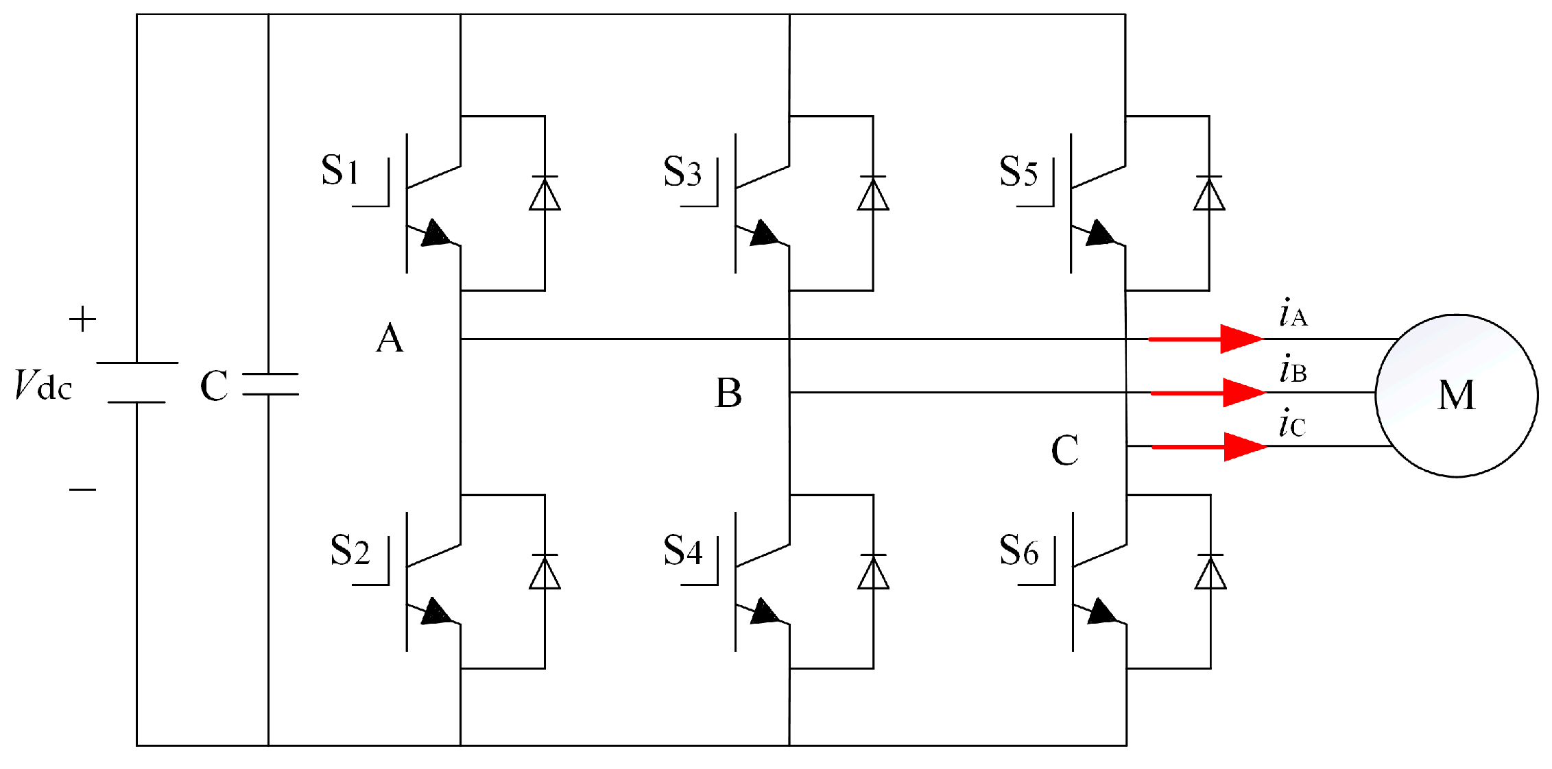
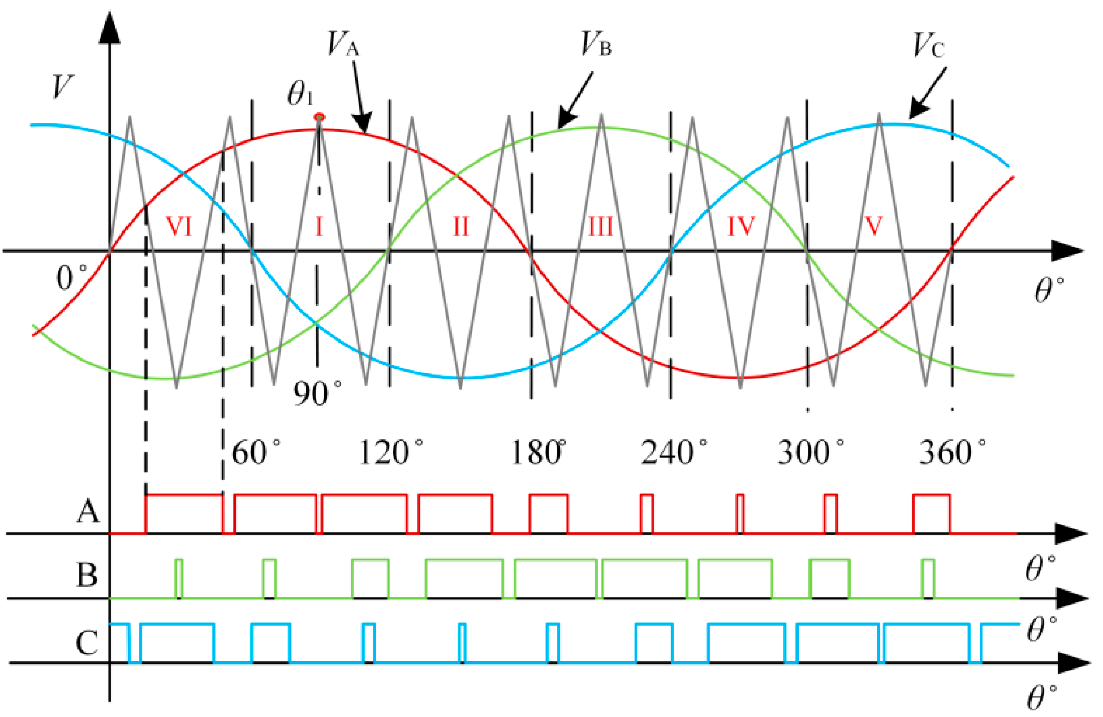
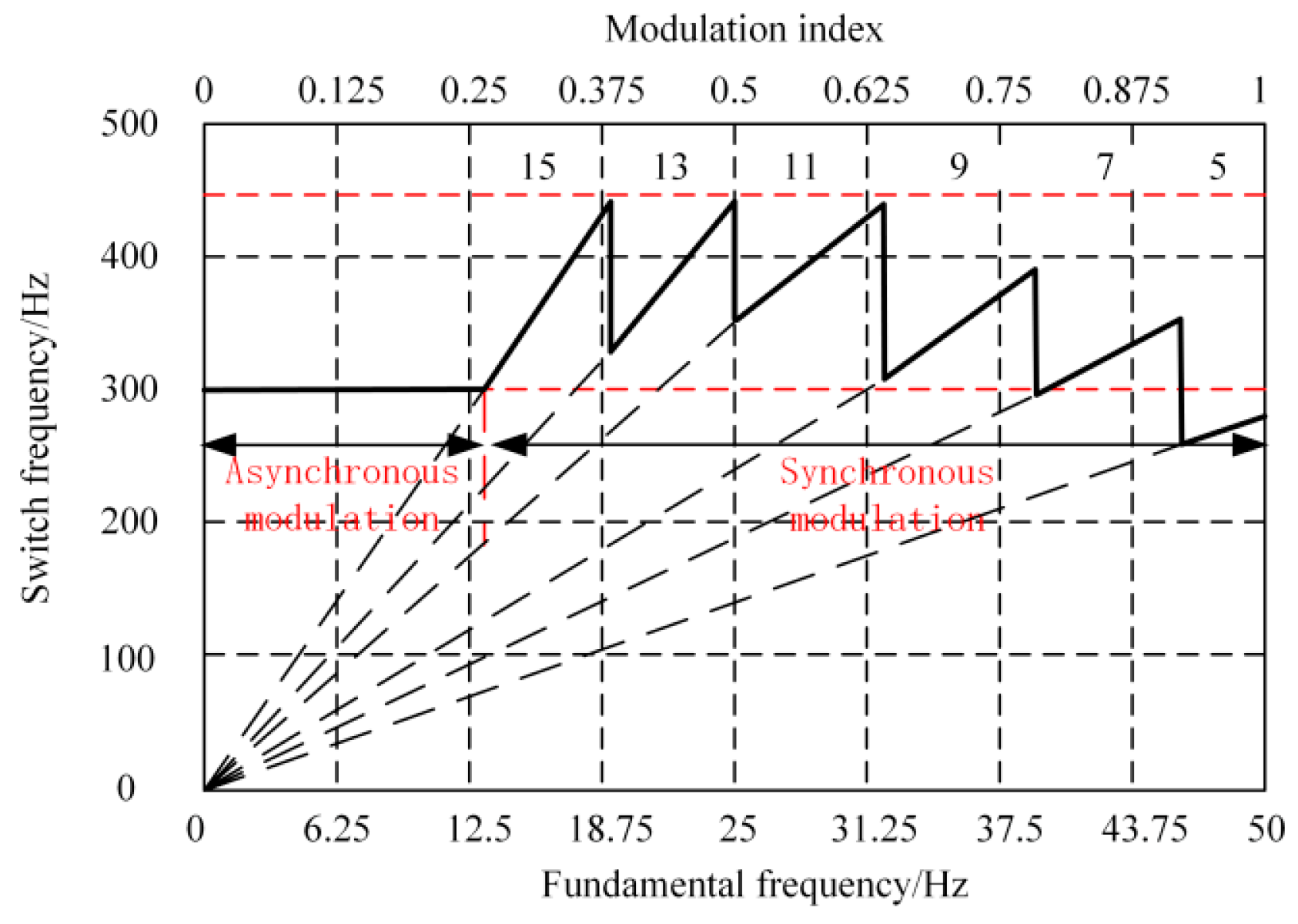
2. Synchronous SPWM
- The angle of each region is 60°.
- The carrier waveform in each adjacent region maintains odd symmetry centered on the boundary.
- The carrier waveform centered on the centerline maintains even symmetry in each region.
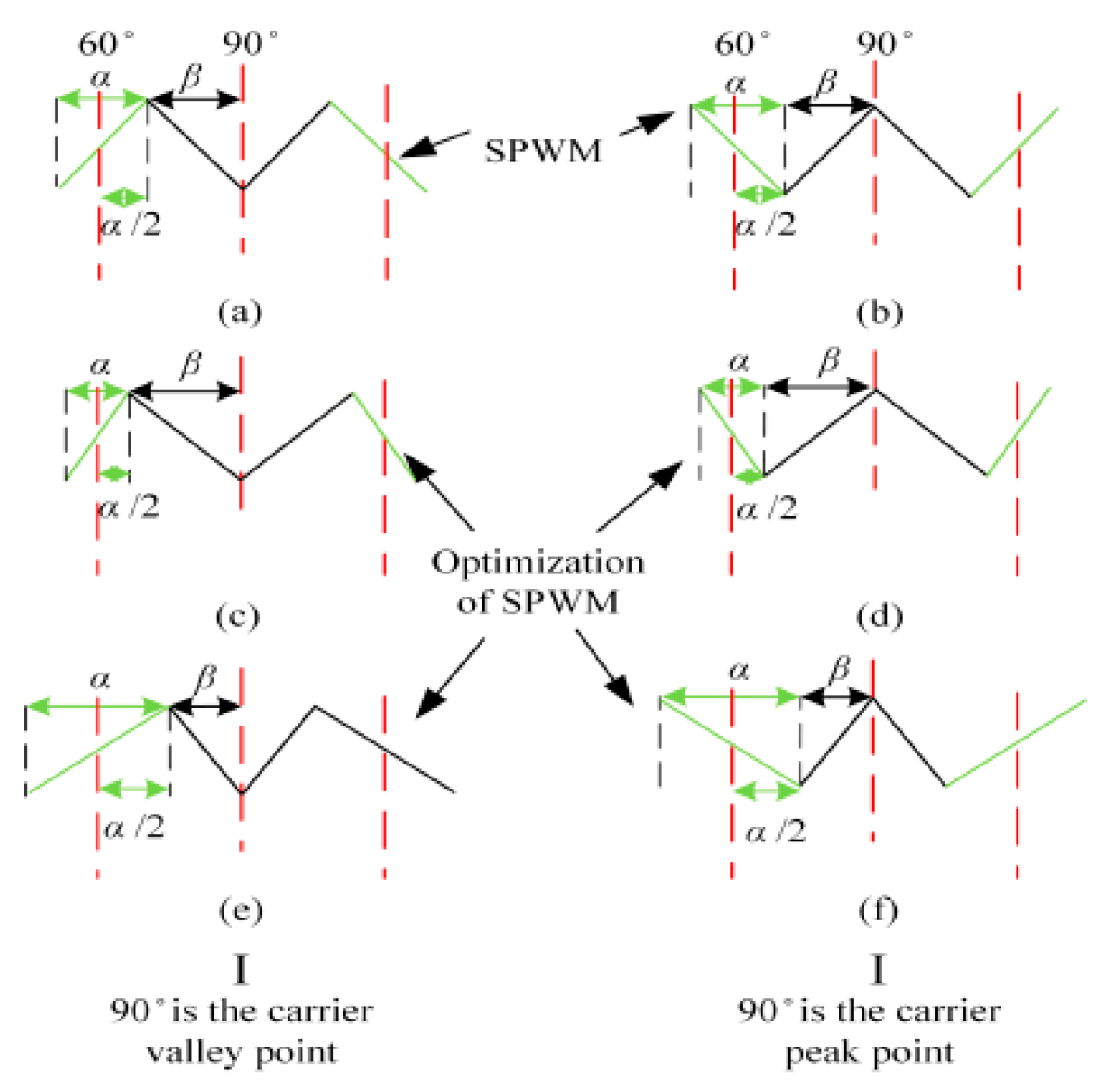
3. Optimal Synchronous SPWM for Unequally Spaced Carriers
3.1. Optimized Synchronous SPWM Carrier Waveform Design Principles for Non-Equally Spaced Carriers
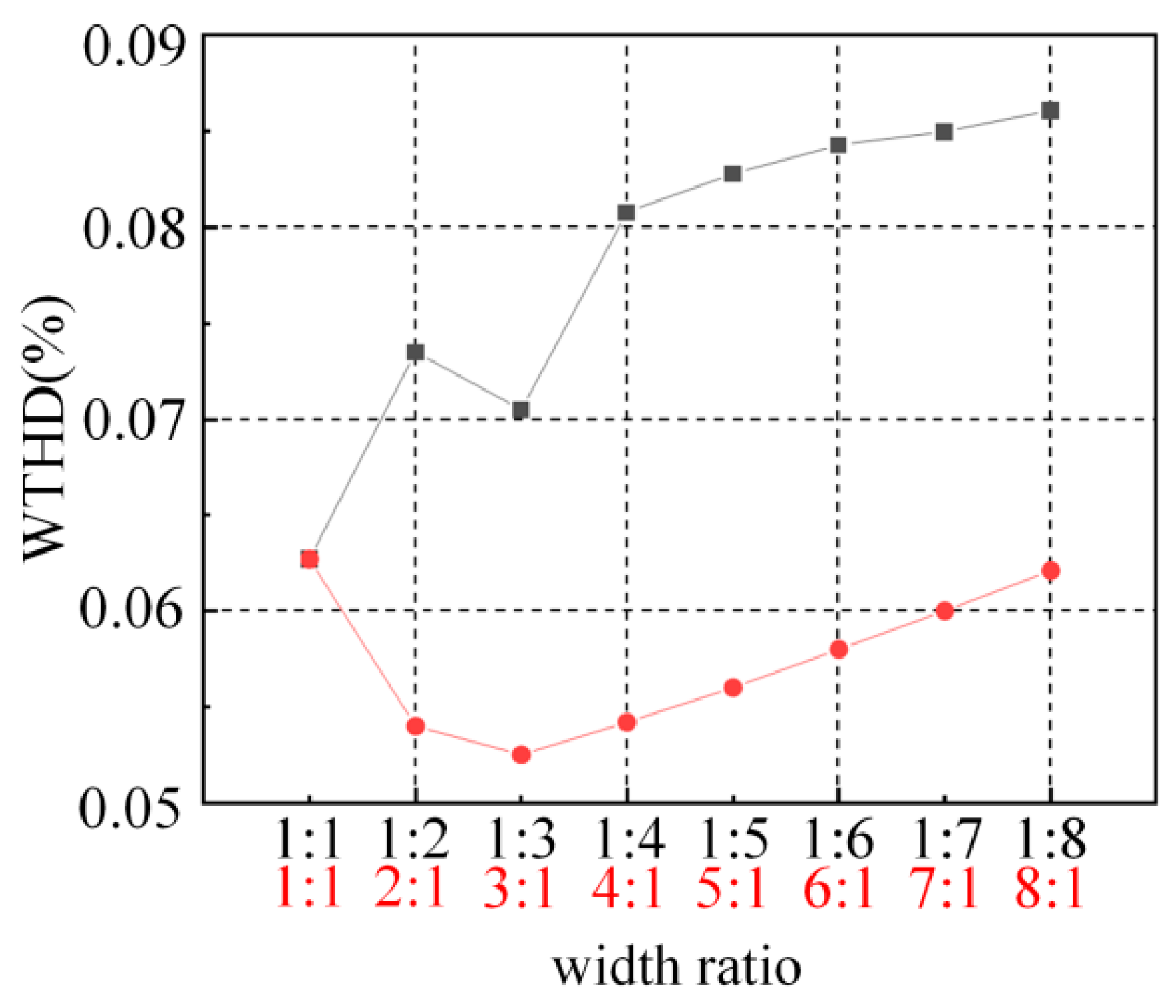
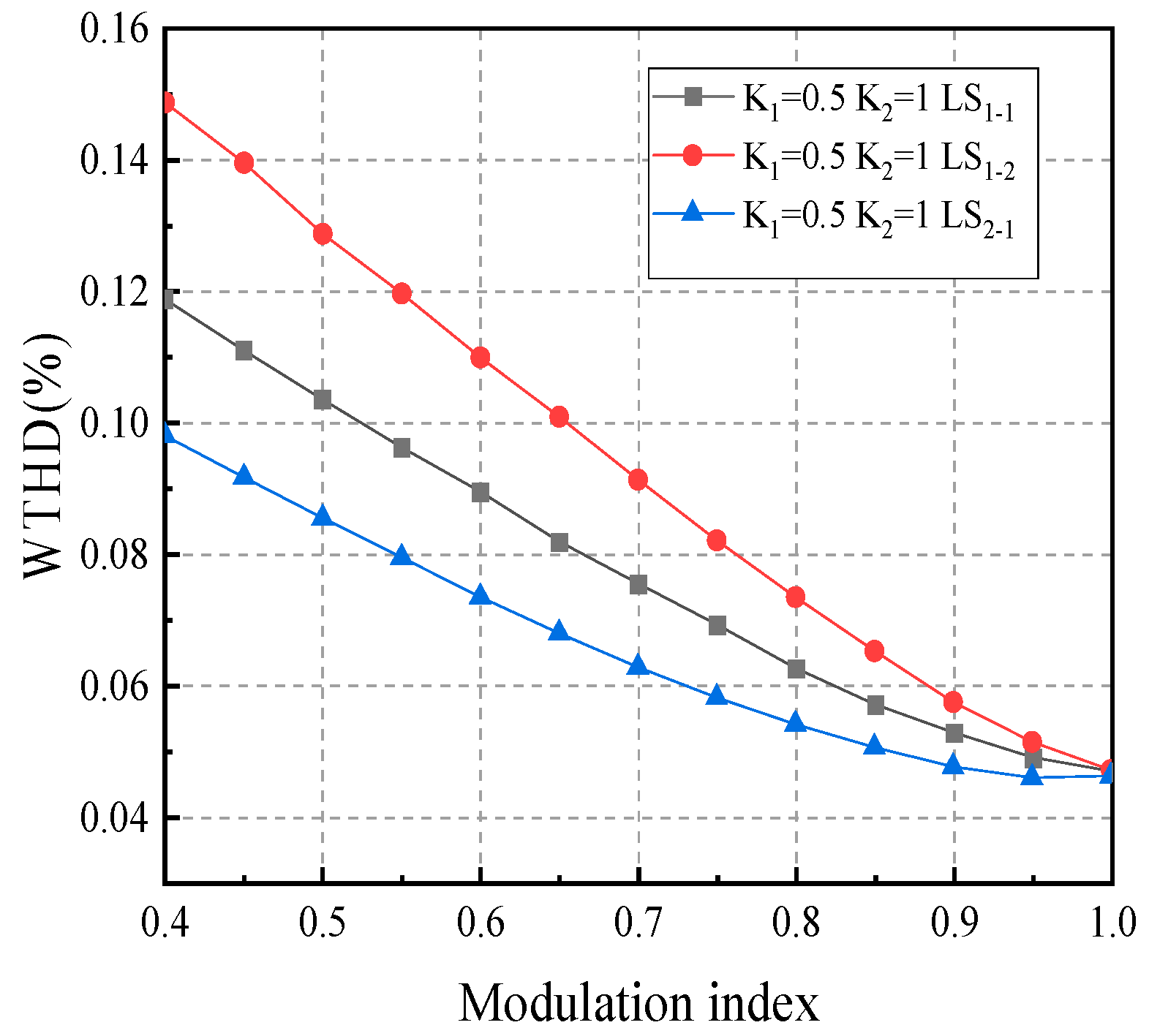
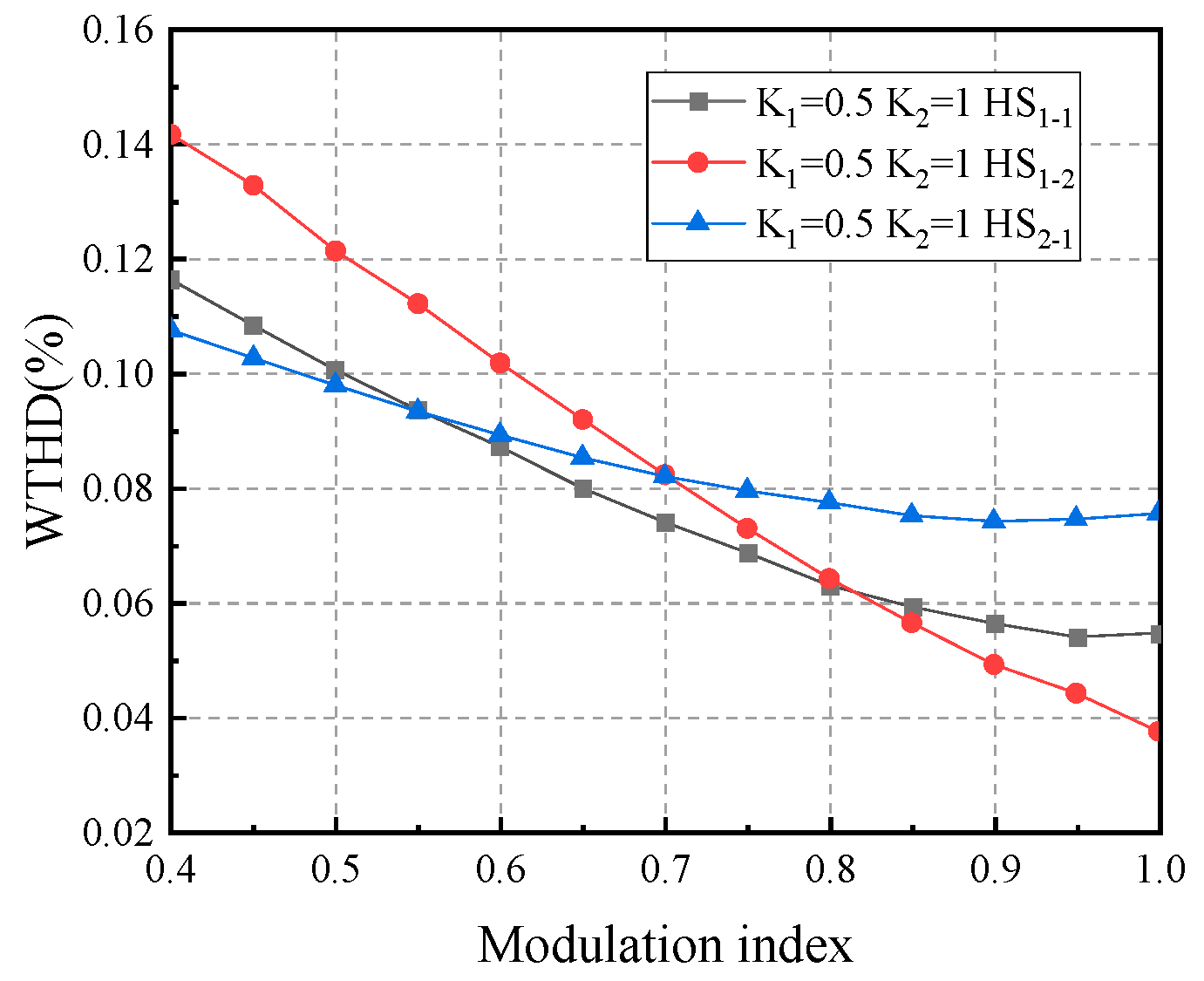
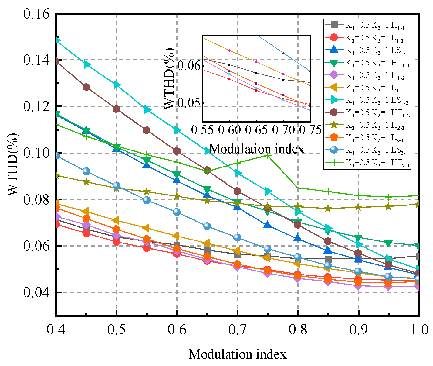
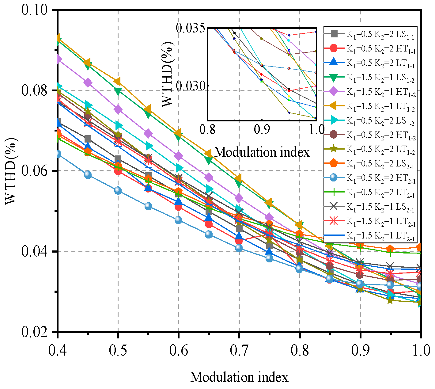
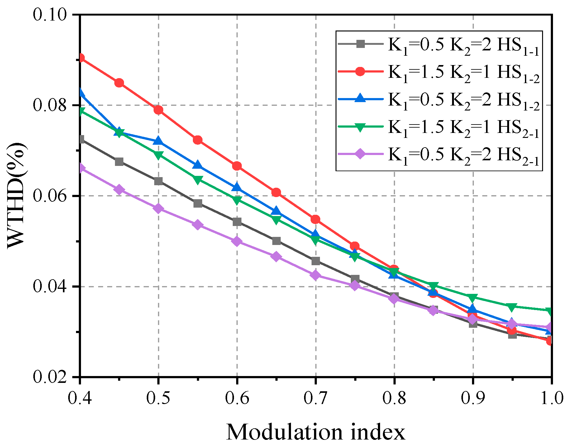
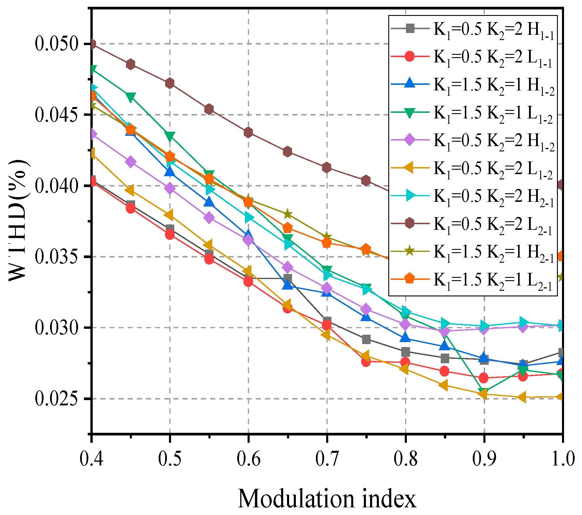
3.2. VWTHD for Different Modulation Strategies
- In each cycle, the carrier wave at the 90° position is noted as H if it is a peak and L if it is a trough.
- Depending on the clamp type, 60° clamp, and 30° clamp are recorded as S and T.
3.3. Multi-Mode Segmented Synchronous Modulation Strategy
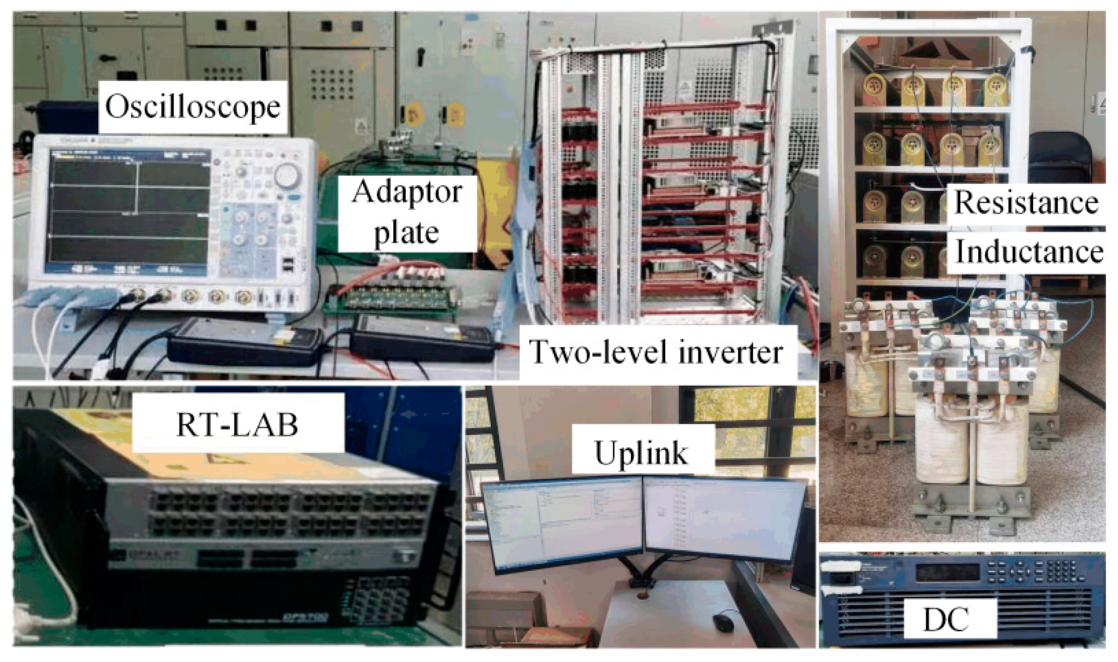
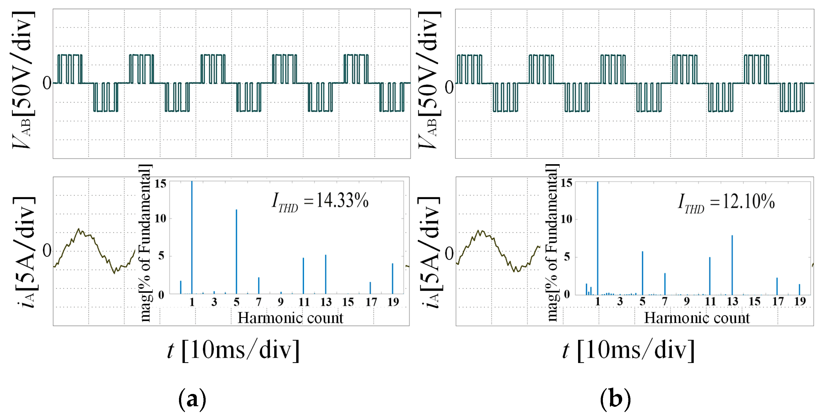
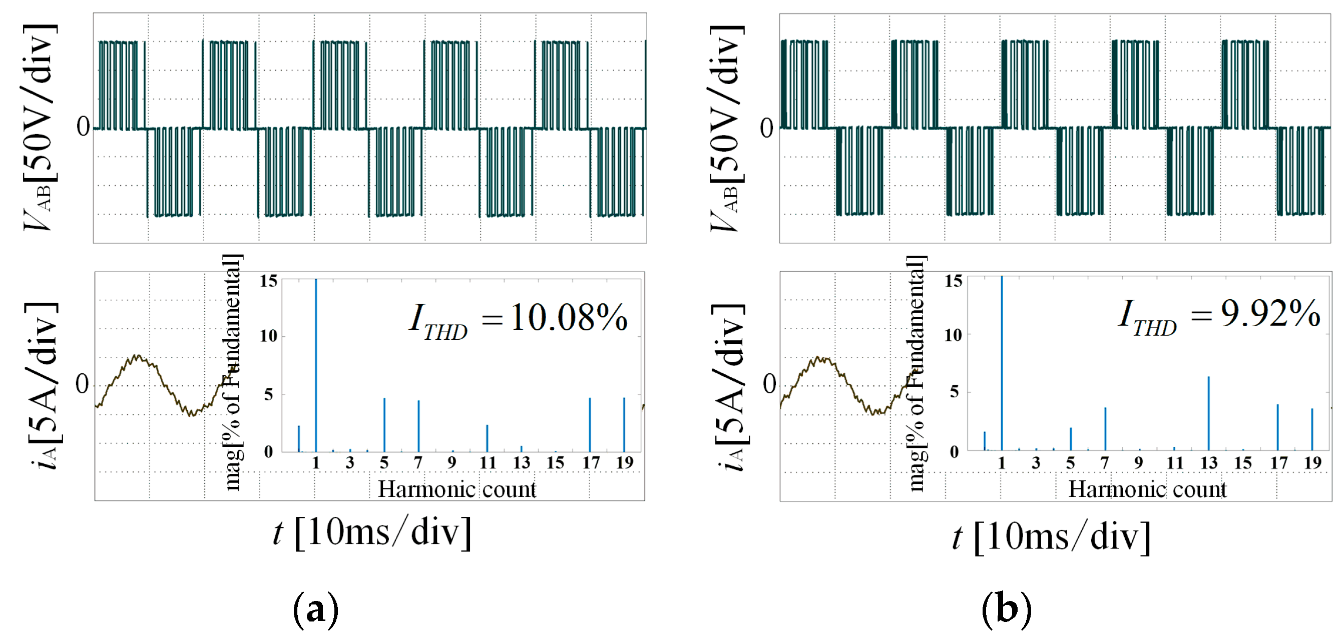
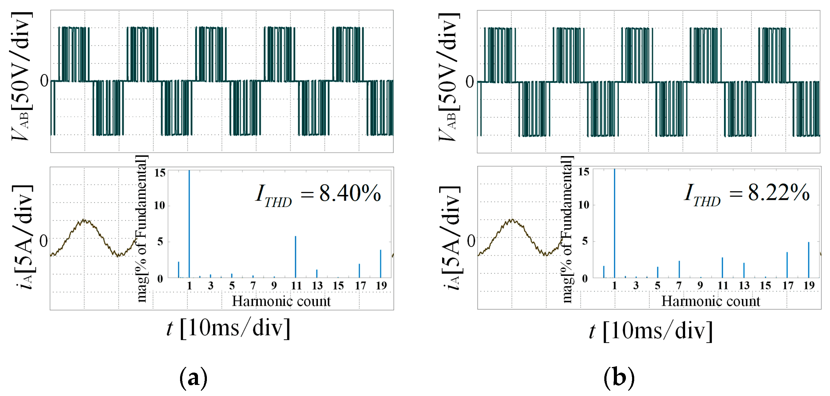
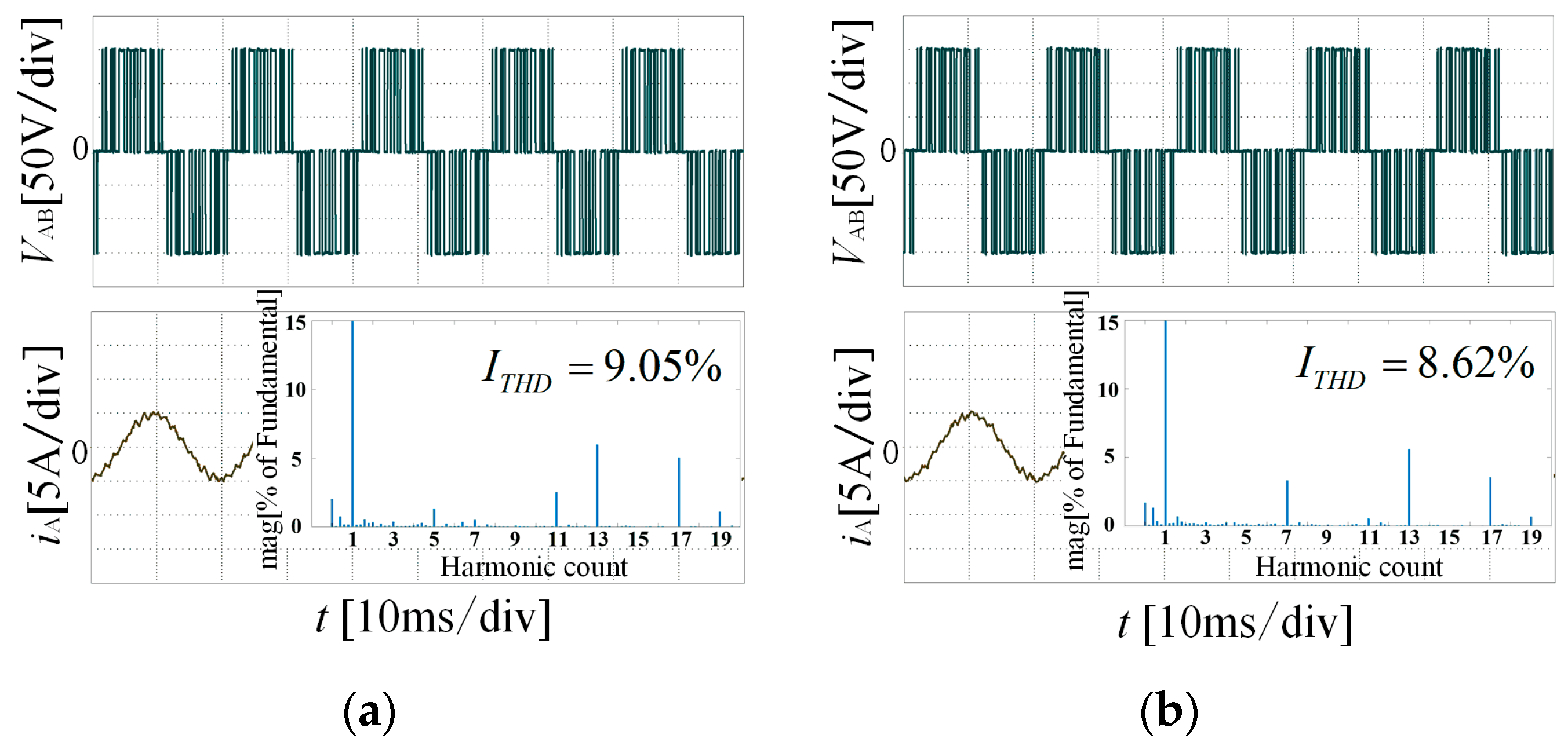
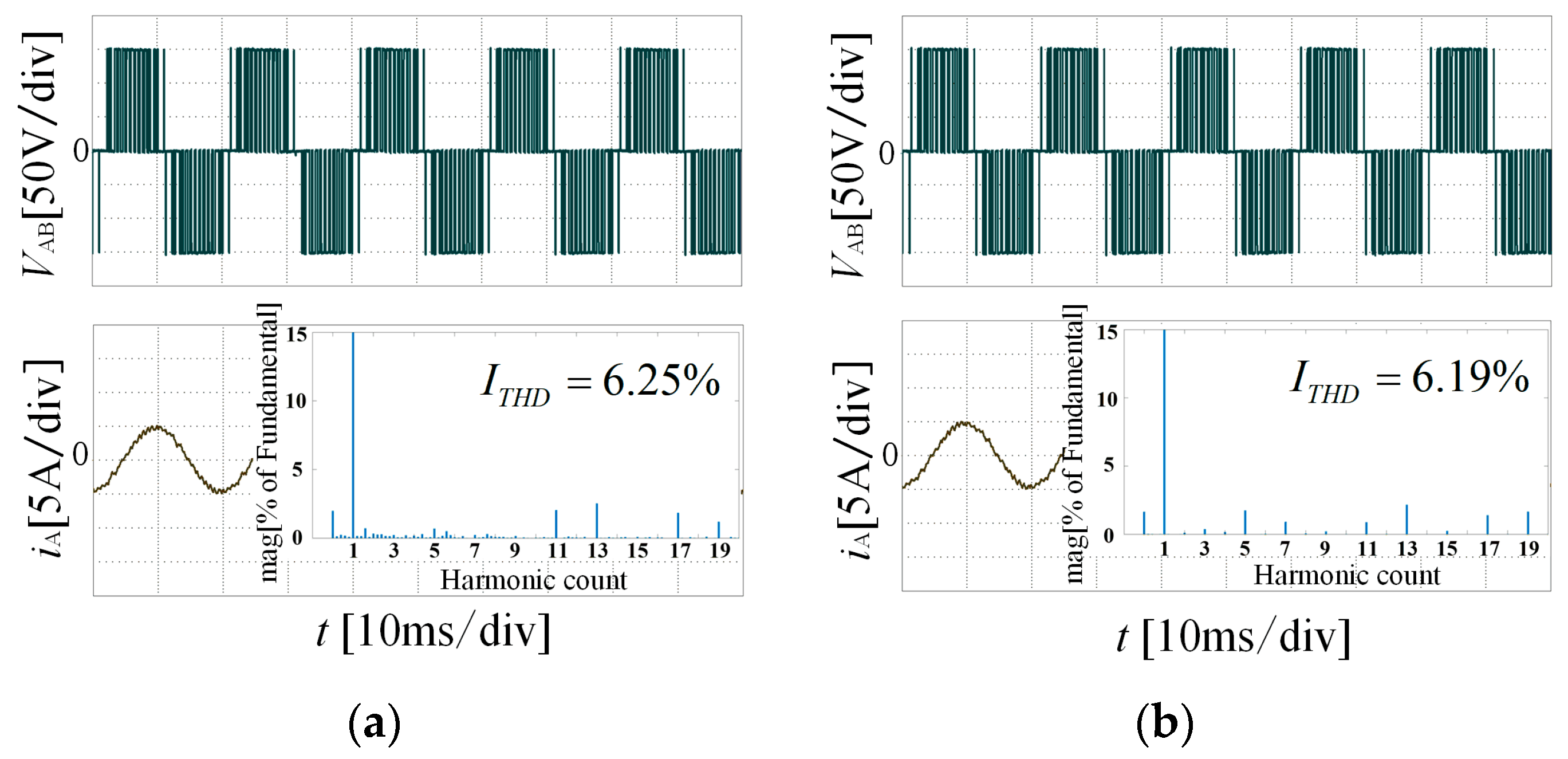
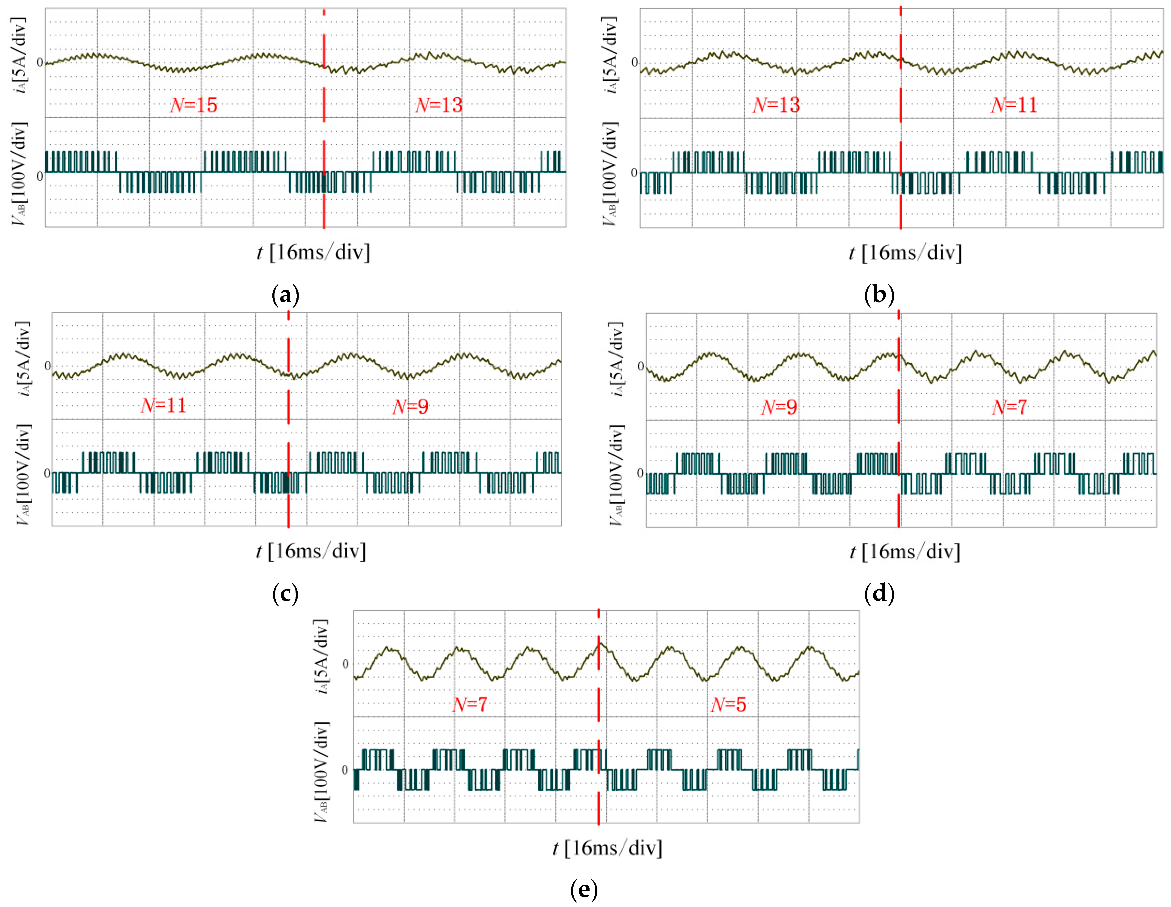
4. Experimental Results and Analysis
5. Conclusions
- Applying the strategy to the closed-loop control of the motor system.
- Combining the modulation algorithm and advanced control strategy proposed in this paper.
Author Contributions
Funding
Institutional Review Board Statement
Informed Consent Statement
Data Availability Statement
Conflicts of Interest
References
- Wang, J.; Miao, Q.; Zhou, X.; Sun, L.; Gao, D.; Lu, H. Current Control Method of Vehicle Permanent Magnet Synchronous Motor Based on Active Disturbance Rejection Control. World Electr. Veh. J. 2023, 14, 2. [Google Scholar] [CrossRef]
- Gao, W.; Zhang, G.; Hang, M.; Cheng, S.; Li, P. Sensorless Control Strategy of a Permanent Magnet Synchronous Motor Based on an Improved Sliding Mode Observer. World Electr. Veh. J. 2021, 12, 74. [Google Scholar] [CrossRef]
- Kang, J.-W.; Hyun, S.-W.; Kan, Y.; Lee, H.; Lee, J.-H. A Novel Zero Dead-Time PWM Method to Improve the Current Distortion of a Three-Level NPC Inverter. Electronics 2020, 9, 2195. [Google Scholar] [CrossRef]
- Vijayakumar, A.; Stonier, A.A.; Peter, G.; Loganathan, A.K.; Ganji, V. Power quality enhancement in asymmetrical cascaded multilevel inverter using modified carrier level shifted pulse width modulation approach. IET Power Electron. 2022, 1–13. [Google Scholar] [CrossRef]
- Xu, W.; Chan, C.H.; Chan, K.W.; Wing, S.; Ho, S.L.; Liu, M. A quantitative harmonics analysis approach for sinusoidal pulse-width-modulation based Z-source inverters. IET Power Electron. 2022, 15, 815–824. [Google Scholar] [CrossRef]
- Liu, J.; Zhang, W.; Xiao, F.; Lian, C.; Gao, S. Six-step mode control of IPMSM for railway vehicle traction eliminating the DC offset in input current. IEEE Trans. Power Electron. 2019, 34, 8981–8993. [Google Scholar] [CrossRef]
- Suhel, S.M.; Maurya, R. A new switching sequences of SVPWM for six-phase induction motor with features of reduced switching losses. CES Trans. Electr. Mach. Syst. 2021, 5, 100–107. [Google Scholar] [CrossRef]
- Yang, Y.-P.; Peng, M.-T. A Surface-Mounted Permanent-Magnet Motor with Sinusoidal Pulsewidth-Modulation-Shaped Magnets. IEEE Trans. Magn. 2019, 55, 2873773. [Google Scholar] [CrossRef]
- Siddique, M.D.; Mekhilef, S.; Padmanaban, S.; Memon, M.A.; Kumar, C. Single-Phase Step-Up Switched-Capacitor-Based Multilevel Inverter Topology with SHEPWM. IEEE Trans. Ind. Appl. 2021, 57, 3107–3119. [Google Scholar] [CrossRef]
- Li, Y.; Zhang, X.-P.; Li, N. An Improved Hybrid PSO-TS Algorithm for Solving Nonlinear Equations of SHEPWM in Multilevel Inverter. IEEE Access 2022, 10, 48112–48125. [Google Scholar] [CrossRef]
- Guan, B.; Doki, S. A Current Harmonic Minimum PWM for Three-Level Converters Aiming at the Low-Frequency Fluctuation Minimum of Neutral-Point Potential. IEEE Trans. Ind. Electron. 2019, 66, 3380–3390. [Google Scholar] [CrossRef]
- Zhang, Z.; Ge, X.; Tian, Z.; Zhang, X.; Tang, Q.; Feng, X. A PWM for Minimum Current Harmonic Distortion in Metro Traction PMSM with Saliency Ratio and Load Angle Constrains. IEEE Trans. Power Electron. 2018, 33, 4498–4511. [Google Scholar] [CrossRef]
- Diao, N.; Sun, X.; Song, C.; Zhang, Q.; Zhang, Z. A Multimodulation Times SVPWM for Dead-Time Effect Elimination in Three-Level Neutral Point Clamped Converters. IEEE Trans. Ind. Electron. 2021, 68, 5476–5485. [Google Scholar] [CrossRef]
- Yan, Q.; Zhang, X.; Zhao, T.; Yuan, X.; Zhao, R. An Analytical Simplified Three-Level SVPWM with Unified Zero-Sequence Component Injection. IEEE Trans. Power Deliv. 2022, 37, 2417–2420. [Google Scholar] [CrossRef]
- Yan, Q.; Zhou, Z.; Wu, M.; Yuan, X.; Zhao, R.; Xu, H. A Simplified Analytical Algorithm in abc Coordinate for the Three-Level SVPWM. IEEE Trans. Power Electron. 2021, 36, 3622–3627. [Google Scholar] [CrossRef]
- Chen, K.-Y.; Xie, Y.-L. Reducing Harmonics Distortion in Five-Phase VSI Using Space-Vector-Based Optimal Hybrid PWM. IEEE Trans. Power Electron. 2017, 32, 2098–2113. [Google Scholar] [CrossRef]
- Yang, H.; Zhang, Y.; Yuan, G.; Walker, P.D.; Zhang, N. Hybrid Synchronized PWM Schemes for Closed-Loop Current Control of High-Power Motor Drives. IEEE Trans. Ind. Electron. 2017, 64, 6920–6929. [Google Scholar] [CrossRef]
- Qiu, Z.; Huang, X.; Ma, K.; Kong, Z.; Liu, X. Sideband Vibro-Acoustic Responses and Improvements with Different Pulsewidth Modulation Strategies in Permanent Magnet Synchronous Motor for Electric Vehicle. IEEE J. Emerg. Sel. Top. Power Electron. 2022, 10, 7098–7108. [Google Scholar] [CrossRef]
- Zhang, G.; Zhou, Z.; Shi, T.; Xia, C. An Improved Multimode Synchronized Space Vector Modulation Strategy for High-Power Medium-Voltage Three-Level Inverter. IEEE Trans. Power Electron. 2021, 36, 4686–4696. [Google Scholar] [CrossRef]
- Sahoo, S.K.; Bhattacharya, T. Phase-Shifted Carrier-Based Synchronized Sinusoidal PWM Techniques for a Cascaded H-Bridge Multilevel Inverter. IEEE Trans. Power Electron. 2018, 33, 513–524. [Google Scholar] [CrossRef]
- Gamoudi, R.; Chariag, D.E.; Sbita, L. A review of spread-spectrum -based PWM technique—A novel fast digital implementation. IEEE Trans. Power Electron. 2018, 33, 10292–10307. [Google Scholar] [CrossRef]
- Drissi, K.E.K.; Luk, P.C.K.; Wang, B.; Fontaine, J. Effects of symmetric distribution laws on spectral power density in randomized PWM. IEEE Power Electron. Lett. 2003, 1, 41–44. [Google Scholar] [CrossRef]
- Xu, J.; Nie, Z.; Zhu, J. Characterization and Selection of Probability Statistical Parameters in Random Slope PWM Based on Uniform Distribution. IEEE Transs. Power Electron. 2021, 36, 1184–1192. [Google Scholar] [CrossRef]
- Huang, Y.; Xu, Y.; Zhang, W.; Zou, J. Hybrid RPWM technique based on modified SVPWM to reduce the PWM acoustic noise. IEEE Trans. Power Electron. 2019, 34, 5667–5674. [Google Scholar] [CrossRef]
- Biswas, S.P.; Anower, M.S.; Sheikh, M.R.I.; Islam, M.R.; Kouzani, A.Z.; Mahmud, M.P. A New Modulation Technique to Improve the Performance of Three Phase Inverters. In Proceedings of the IEEE International Conference on Applied Superconductivity and Electromagnetic Devices, Tianjin, China, 16–18 October 2020; pp. 1–2. [Google Scholar]
- Rathore, A.K.; Holtz, J.; Boller, T. Synchronous Optimal Pulsewidth Modulation for Low-Switching-Frequency Control of Medium-Voltage Multilevel Inverters. IEEE Trans. Ind. Electron. 2010, 57, 2374–2381. [Google Scholar] [CrossRef]


| N | K1, K2 | Modulation Strategy |
|---|---|---|
| 5 | K1 = 0.5, K2 = 1 | LT1–1, LT1–2, LT2–1 |
| 7 | K1 = 0.5, K2 = 1 | HS1–1, HS1–2, HS2–1 |
| 9 | K1 = 0.5, K2 = 1 | H1–1, L1–1, LS1–1, HT1–1, H1–2, L1–2, LS1–2, HT1–2, H2–1, L2–1, LS2–1, HT2–1 |
| 11 | K1 = 0.5, K2 = 2 | LS1–1, HT1–1, LT1–1, LS1–2, HT1–2, LT1–2, LS2–1, HT2–1, LT2–1 |
| K1 = 1.5, K2 = 1 | LS1–2, HT1–2, LT1–2, LS2–1, HT2–1, LT2–1 | |
| 13 | K1 = 0.5, K2 = 2 | HS1–1, HS1–2, HS2–1 |
| K1 = 1.5, K2 = 1 | HS1–2, HS2–1 | |
| 15 | K1 = 0.5, K2 = 2 | H1–1, L1–1, H1–2, L1–2, H2–1, L2–1 |
| K1 = 1.5, K2 = 1 | H1–2, L1–2, H2–1, L2–1 |
| N | K1, K2 | Optimal Modulation Strategy |
|---|---|---|
| 5 | K1 = 0.5, K2 = 1 | LT2–1 |
| 7 | K1 = 0.5, K2 = 1 | HS1–1 |
| 9 | K1 = 0.5, K2 = 1 | L1–1 |
| 11 | K1 = 0.5, K2 = 2 | HT2–1 |
| 13 | K1 = 0.5, K2 = 2 | HS2–1 |
| 15 | K1 = 0.5, K2 = 2 | L1–1 |
| Parameter | Values | Unit |
|---|---|---|
| DC-side capacitance/C | 780 | μF |
| DC-link voltage/Vdc | 150 | V |
| Load resistance/R | 10 | Ω |
| Load inductance/L | 20 | mH |
| Fundamental frequency/f | 50 | Hz |
| Dead-time/t | 600 | ns |
Disclaimer/Publisher’s Note: The statements, opinions and data contained in all publications are solely those of the individual author(s) and contributor(s) and not of MDPI and/or the editor(s). MDPI and/or the editor(s) disclaim responsibility for any injury to people or property resulting from any ideas, methods, instructions or products referred to in the content. |
© 2023 by the authors. Licensee MDPI, Basel, Switzerland. This article is an open access article distributed under the terms and conditions of the Creative Commons Attribution (CC BY) license (https://creativecommons.org/licenses/by/4.0/).
Share and Cite
Jin, X.; Li, S.; Sun, W.; Chen, W.; Gu, X.; Zhang, G. Optimized Synchronous SPWM Modulation Strategy for Traction Inverters Based on Non-Equally Spaced Carriers. World Electr. Veh. J. 2023, 14, 157. https://doi.org/10.3390/wevj14060157
Jin X, Li S, Sun W, Chen W, Gu X, Zhang G. Optimized Synchronous SPWM Modulation Strategy for Traction Inverters Based on Non-Equally Spaced Carriers. World Electric Vehicle Journal. 2023; 14(6):157. https://doi.org/10.3390/wevj14060157
Chicago/Turabian StyleJin, Xuefeng, Shiwei Li, Wenbo Sun, Wei Chen, Xin Gu, and Guozheng Zhang. 2023. "Optimized Synchronous SPWM Modulation Strategy for Traction Inverters Based on Non-Equally Spaced Carriers" World Electric Vehicle Journal 14, no. 6: 157. https://doi.org/10.3390/wevj14060157