Article

Optimization of TSPWM for Common-Mode Voltage Reduction in Vehicular Electric Drive System

School of Automotive and Transportation Engineering, Hefei University of Technology, Tunxi Road 193, Hefei 230009, China
*
Author to whom correspondence should be addressed.
World Electr. Veh. J. 2022, 13(1), 5; https://doi.org/10.3390/wevj13010005
Submission received: 11 November 2021 / Revised: 17 December 2021 / Accepted: 23 December 2021 / Published: 24 December 2021

Abstract

:
Common-mode voltage can be reduced effectively by optimized modulation methods without increasing additional costs. However, the existing methods cannot satisfy the requirements of the vehicular electric-drive application. This paper optimizes the tri-state voltage modulation method to reduce the common-mode voltage for vehicular electric drive system applications. Firstly, the discontinuous switching issue during sector transition is analyzed. Under the limit of two switching times in one period, multiple alignments combination is proposed to address that issue. Secondly, the zero-voltage time intervals in different modulation ranges are explored. This paper proposes an unsymmetric translation method to reconstruct the voltage vector, and then the minimum zero-voltage time interval is controlled to enough value for safe switching. Finally, the proposed methods have been validated through experiments on a vehicular electric drive system. The results show that the common-mode voltage can be reduced effectively in the whole range with the optimized tri-state voltage modulation method.

1. Introduction

The conventional space vector pulse width modulation (SVPWM) has been widely applied to the vehicular electric drive system, as it performs well in terms of voltage linearity, current harmonics, and system efficiency [1,2]. However, since the introduction of the zero vectors of 000 and 111, the corresponding amplitude of the common-mode voltage (CMV) is equal to Vdc/2 (the DC bus voltage) [3]. On the one hand, the excessively high CMV will lead to poor electromagnetic compatibility (EMC) performance [4]. On the other hand, the common-mode voltage will break down the bearing oil film and generate shaft currents, which can corrode the bearing and seriously affect the noise, vibration, and harshness (NVH) and safety performance of the electric drive system [5].
The CMV fluctuation can be reduced by hardware or software methods. The hardware solutions, such as adding filters or adopting complex topologies, will increase the cost and size of the electric drive system [6]. On the contrary, the software solutions adjusting the voltage modulation strategies are more flexible and applied widely [7,8]. According to the selection of voltage space vectors, the reduction of common-mode voltage (RCMV) methods include the active zero state PWM (AZSPWM1, AZSPWM2, AZSPWM3) [9], remote state PWM (RSPWM) [10], near state PWM (NSPWM [11]), TSPWM [12,13]. Both these RCMV methods can reduce the maximum CMV of conventional SVPWM from Vdc/2 to Vdc/6, and then decrease the negative effect of CMV on the EMC and shaft corrosion. However, most RCMV methods have bipolar line-to-line voltage patterns, require simultaneous switching, and cause significant voltage harmonics, which is not suitable for practical application. Among those RCMV methods, the TSPWM performs best in the whole modulation range, harmonic proportion, and system efficiency [14]. Thus, this paper will optimize the TSPWM method and apply it to the CMV reduction of the vehicular electric drive system.
The main contributions of this paper are shown as follows:
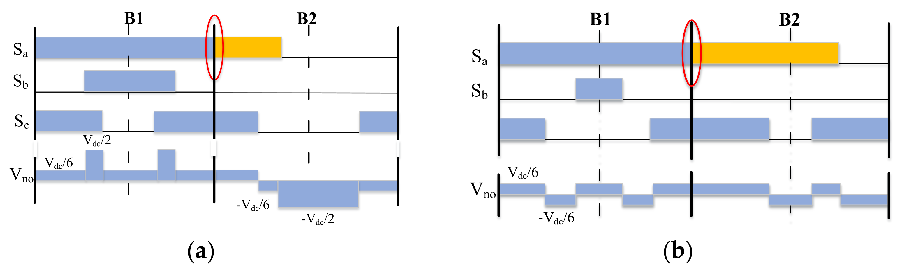
  • The standard TSPWM needs to switch three times in one period when the voltage vector transit from one sector to another, which is not suitable for vehicular electric drive applications. This paper combines different alignment technology in the sector transition process. The switch times are reduced to one while the CMV can keep low in the whole control range.
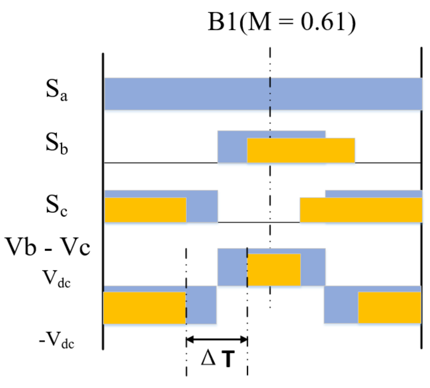
  • In the standard TSPWM, the minimum zero-voltage time interval between line-to-line voltage pulse reversals is close to zero in the border between the high and low region of TSPWM, which causes overvoltage and can be dangerous in a vehicular electric drive application. This paper proposes an unsymmetric translation method to reconstruct the voltage vector, and then the minimum zero-voltage time interval is controlled to a safe lower limit.
The rest of this paper is as follows: Section 2 makes a simple review of the existing TSPWM technology; Section 3 analyzes two issues of the standard TSPWM, and then proposes the corresponding solutions for each issue respectively; Section 4 compares the experimental results with or without the proposed methods; Section 5 discusses the work of this paper and makes a further research plan.

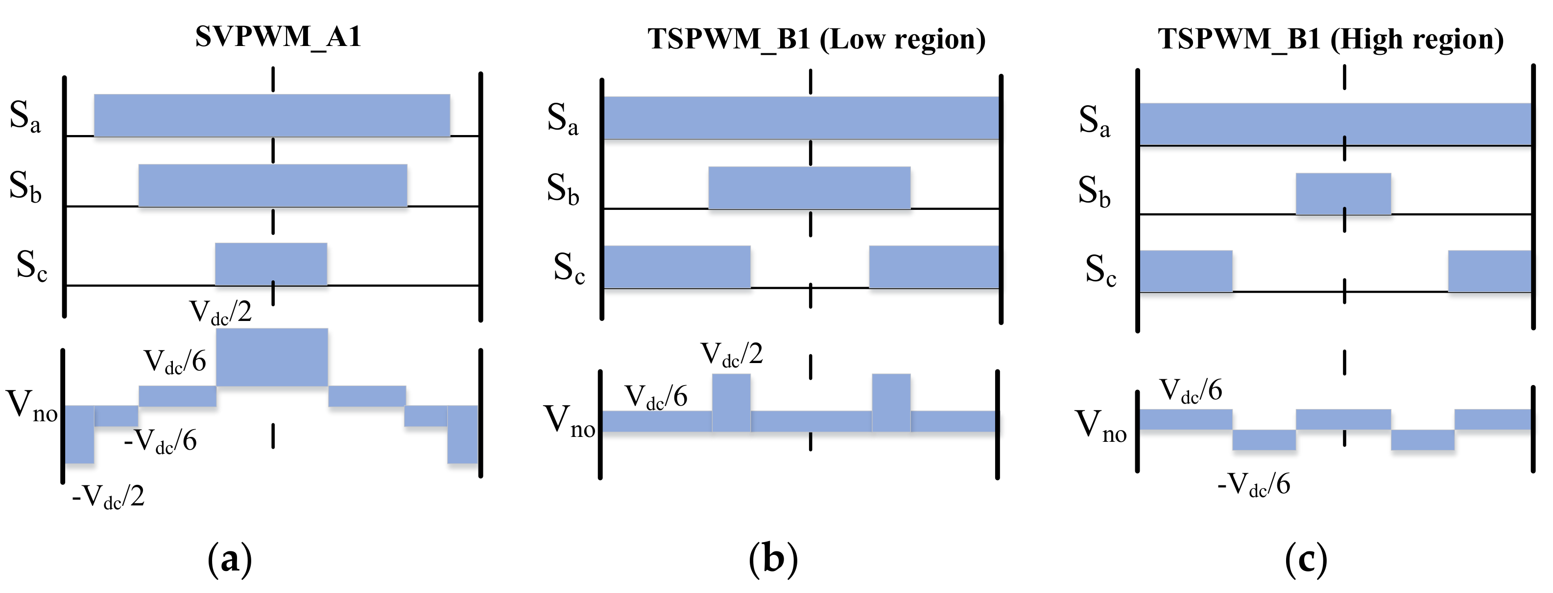
2. Review of the Existing TSPWM Technology

The topology of the conventional three-phase electric drive system is shown in Figure 1. CMV of the system is defined as the voltage difference between the neutral point of the electric machine (n) and the midpoint of dc voltage (o); the phase voltages can represent this:
V n o = V a o + V b o + V c o 3
When the conventional SVPWM is applied, the output voltages can be divided into six different voltage sectors depending on the selected primary voltage vectors. As shown in Figure 2a, in the voltage sector A1, the output voltages are generated by combing the basic voltage vectors V4 (100) and V6 (110). While in the TSPWM method, all the voltage sectors have 30 degrees ahead compared to the conventional SVPWM, as shown in Figure 2b.
In the standard TSPWM technology, the switch patterns can be divided based on the modulation factor. As shown in Figure 3, in the B1 voltage sector, the desired output voltage vector is constructed by two primary voltage vectors and the zero-voltage vector in the low modulation region. While in the high modulation region, three nearest voltage vectors are applied together to construct the desired output voltage vector.
The CMV of SVWPM and TSPWM in different regions are compared in Figure 4. The fluctuation amplitude of CMV with conventional SVPWM is much larger than the TSPWM, with Vdc and Vdc/3, respectively. Besides, although the maximum CMV value with the TSPWM in the low region reaches Vdc/2, the minimum CMV is Vdc/6. The whole fluctuation of CMV in the B1 voltage sector can remain under Vdc/3. The more considerable CMV fluctuation will only occur in the sector switching time. Moreover, the maximum CMV and CMV fluctuation keep low for the CMV with TSPWM in the high region. In short, with the TSPWM method, the CMV can be reduced to a relatively low range, which is beneficial for suppressing EMC and shaft corrosion.
However, in the standard TSPWM strategy, three switching times in one period are needed when the voltage vector transitions from one sector to another. Besides, the zero-voltage time interval between line-to-line voltage pulse reversals can be too small when the modulation factor is close to the boundary between the high and low regions. Both these two aspects cannot satisfy the requirements of the electric drive system. Thus, in the following parts of this paper, these two problems of TSPWM are discussed, and the corresponding optimization solution is developed to address these issues.

3. Optimization of TSPWM

3.1. Discontinuous Switching between Different Sectors

In Figure 5a, the discontinuous switching phenomenon of TSPWM in the low region is represented. In the standard TSPWM, the switch state of Sa at the end of sector B1 is high, but it changes to low at the beginning of sector B2. When the voltage vector changes to sector B2, the state of Sa should switch to low immediately and then switches on and off by following the regular instructions. Thereby, three switch times are needed in one period, leading to additional switching loss and voltage spike, and the actual output voltage vector also has a slight deviation from the desired output voltage. Similarly, the discontinuous switching phenomenon will occur in the high region with the standard TSPWM method, as shown in Figure 5b.
In Figure 6, the left-alignment configuration of Sa is applied in the sector transition time to solve this issue. Then only one switch time is needed in sector B2, and as the switch on the duty of Sa is the same as the standard central-alignment configuration, the average output voltage has no deviation to the desired voltage. Simultaneously, the fluctuation of the CMV is as slight as the standard TSPWM. Please notice that only in the transition time, the left-alignment configuration is utilized, and then for the following voltage vector in the B2 sector, the standard central alignment will be reused to achieve better harmonic performance. Besides, the right alignment should also be applied for the transit between another voltage sector.

3.2. Increase Zero-Voltage Time Interval

For the conventional SVPWM, the zero-voltage time interval between line-to-line voltage pulse reversals can always stay at a relatively large value. As shown in Figure 7, the line-to-line voltage pulse reversal only occurs between two dependent PWM periods. Moreover, since the maximum switch-on time of every phase is smaller than one period, the Δ T in Figure 6 is much larger than zero. Thereby, for the conventional SVPWM, the zero-voltage time interval will not occur, which is also an essential advantage of that modulation method.
As for the TSPWM, the voltage-time interval Δ T can keep large in both the low and high modulation factor region, which is shown in Figure 8a,c. However, the Δ T can be zero when the modulation factor equals 0.61. The overvoltage caused by the zero-voltage time interval is dangerous for the vehicular electric drive system.
To address this problem, a novel switch configuration is developed. As shown in Figure 9, the on–off switch time of Sb is moved in the right direction, while the on–off switch time of Sc is moved in the left direction. Moreover, in the moving process, the switch-on time of Sb and Sc are not changed to guarantee the output voltage is the same as the desired voltage. Then, the voltage time interval Δ T can be about twice the moving time length. The Δ T is determined by the dead time and switch characteristics of electric drive, and its value can be calibrated in practical application.

4. Experiment

To validate these two optimization methods of TSPWM, a simulation platform including modulation strategy, inverter model, standard voltage model, and bearing voltage model is established in MATLAB/Simulink. The shaft voltage model is constructed through some equivalent capacitances, in which the Csf denotes the capacitance between stator winding and machine housing, the Csr denotes the capacitance between stator winding and rotor, the Crf denotes the capacitance between the rotor and machine housing. The Cb and Rb denote the capacitance and resistance of bearing oil film. The corresponding parameters of the simulation platform are shown in Table 1.
Firstly, the optimization for discontinuous switching between different sectors has been validated. In Figure 10, the CMV of the conventional SVPWM and optimized TSPWM in low modulation factor (0.2) are compared. By combing the left-alignment, central-alignment, right-alignment, the switching times in one period can be controlled equal to or less than two. At the same time, the CMV of the optimized TSPWM has the same performance as the standard TSPWM, with only 1/3 of the conventional SVPWM. Besides, the CMV performance in high modulation factor (0.8) is also demonstrated, as shown in Figure 11. The CMV fluctuation has been suppressed effectively from ±180 V to about ±60 V.
Secondly, the bearing voltage with different modulation methods is also obtained via the bearing voltage equivalent model. The bearing voltage is about 1/60 of the CMV. The wave of bearing voltage has the same change law as the CMV. Thus, as shown in Figure 12 and Figure 13, the bearing voltage fluctuation with the optimized TSPWM method is about 1/3 of the bearing voltage with the SVPWM, and the corresponding values are ±3 V and ±1 V, respectively.
At last, the optimization for zero-voltage time intervals with the TSPWM method has been validated. In Figure 14, the line–line voltage Vab wave when the modulation factor is 0.6 is shown. From the enlarged view, we can notice that the minimum voltage pulse reversals can be zero at some points, which is extremely dangerous for the vehicular electric drive system. Then, the Vab with an optimized TSPWM strategy is tested. Setting the moving time length for each phase to 5 μs, the minimum voltage pulse reversals are expanded to about 6 μs, as shown in Figure 15.

5. Conclusions

This paper focuses on the application problem of TSPWM to the vehicular electric drive system. It then optimizes the standard TSPWM to address two issues: discontinuous switching between different sectors and the zero-voltage time interval between voltage pulse reversals. The validation of the proposed methods is carried out in a simulation platform. The results show that with the proposed strategies in this paper, the CMV can be reduced to one-third of the SVPWM without additional switching and the zero-voltage time interval. Thus, the methods effectively promote the TSPWM on vehicular applications by reducing EMC and improving bearing life. Further work will be implemented to test the proposed strategies in a practical test bench and explore the efficiency and harmonic characteristics of TSPWM.

Author Contributions

Conceptualization, S.J.; Methodology, S.J.; Software, Y.W.; Validation, Y.W.; Writing—original draft, S.J.; All authors have read and agreed to the published version of the manuscript.

Funding

This research was supported by Special Funds for Fundamental Research Expenses of Central Universities: Academic Newcomer Promotion Plan (JZ2021HGTA0162), and Scientific Research and Innovation Start Special (JZ2021HGQA0237).

Institutional Review Board Statement

Not applicable.

Informed Consent Statement

Not applicable.

Conflicts of Interest

The authors declare no conflict of interest.

References

  1. Zhu, Y.; Xiao, M.; Su, X.; Yang, G.; Lu, K.; Wu, Z. Modeling of conduction and switching losses for IGBT and FWD based on SVPWM in automobile electric drives. Appl. Sci. 2020, 10, 4539. [Google Scholar] [CrossRef]
  2. Kolli, A.; Béthoux, O.; De Bernardinis, A.; Labouré, E.; Coquery, G. Space-vector PWM control synthesis for an H-bridge drive in electric vehicles. IEEE Trans. Veh. Technol. 2013, 62, 2441–2452. [Google Scholar] [CrossRef]
  3. Jayaraman, K.; Kumar, M. Design of passive common-mode attenuation methods for inverter-fed induction motor drive with reduced common-mode voltage PWM technique. IEEE Trans. Power Electron. 2019, 35, 2861–2870. [Google Scholar] [CrossRef]
  4. Li, G.; Pommerenke, D.; Min, J. A low frequency electric field probe for near-field measurement in EMC applications. In Proceedings of the 2017 IEEE International Symposium on Electromagnetic Compatibility & Signal/Power Integrity (EMCSI), Washington, DC, USA, 7–11 August 2017; pp. 498–503. [Google Scholar]
  5. Hu, W.; Ruan, C.; Nian, H.; Sun, D. Zero-sequence current suppression strategy with common-mode voltage control for open-end winding PMSM drives with common DC bus. IEEE Trans. Ind. Electron. 2020, 68, 4691–4702. [Google Scholar] [CrossRef]
  6. Baik, J.H.; Yun, S.W.; Kim, D.S.; Kwon, C.K.; Yoo, J.Y. EMI noise reduction with new active zero state PWM for integrated dynamic brake systems. J. Power Electron. 2018, 18, 923–930. [Google Scholar]
  7. Qin, C.; Zhang, C.; Chen, A.; Xing, X.; Zhang, G. A space vector modulation scheme of the quasi-Z-source three-level T-type inverter for common-mode voltage reduction. IEEE Trans. Ind. Electron. 2018, 65, 8340–8350. [Google Scholar] [CrossRef]
  8. Dabour, S.M.; Abdel-Khalik, A.S.; Massoud, A.M.; Ahmed, S. Analysis of scalar PWM approach with optimal common-mode voltage reduction technique for five-phase inverters. IEEE J. Emerg. Sel. Top. Power Electron. 2018, 7, 1854–1871. [Google Scholar] [CrossRef] [Green Version]
  9. Hava, A.M.; Ün, E. Performance analysis of reduced common-mode voltage PWM methods and comparison with standard PWM methods for three-phase voltage-source inverters. IEEE Trans. Power Electron. 2009, 24, 241–252. [Google Scholar] [CrossRef]
  10. Hava, A.M.; Ün, E. A high-performance PWM algorithm for common-mode voltage reduction in three-phase voltage source inverters. IEEE Trans. Power Electron. 2010, 26, 1998–2008. [Google Scholar] [CrossRef]
  11. Un, E.; Hava, A.M. A near-state PWM method with reduced switching losses and reduced common-mode voltage for three-phase voltage source inverters. IEEE Trans. Ind. Appl. 2009, 45, 782–793. [Google Scholar] [CrossRef]
  12. Lu, H.; Qu, W.; Cheng, X.; Fan, Y.; Zhang, X. A novel PWM technique with two-phase modulation. IEEE Trans. Power Electron. 2007, 22, 2403–2409. [Google Scholar] [CrossRef]
  13. Lu, H.; Cheng, X.; Qu, W.; Sheng, S.; Li, Y.; Wang, Z. A three-phase current reconstruction technique using single DC current sensor based on TSPWM. IEEE Trans. Power Electron. 2013, 29, 1542–1550. [Google Scholar]
  14. Xu, J.; Han, J.; Wang, Y.; Ali, M.; Tang, H. High-frequency SiC three-phase VSIs with common-mode voltage reduction and improved performance using novel tri-state PWM method. IEEE Trans. Power Electron. 2018, 34, 1809–1822. [Google Scholar] [CrossRef]
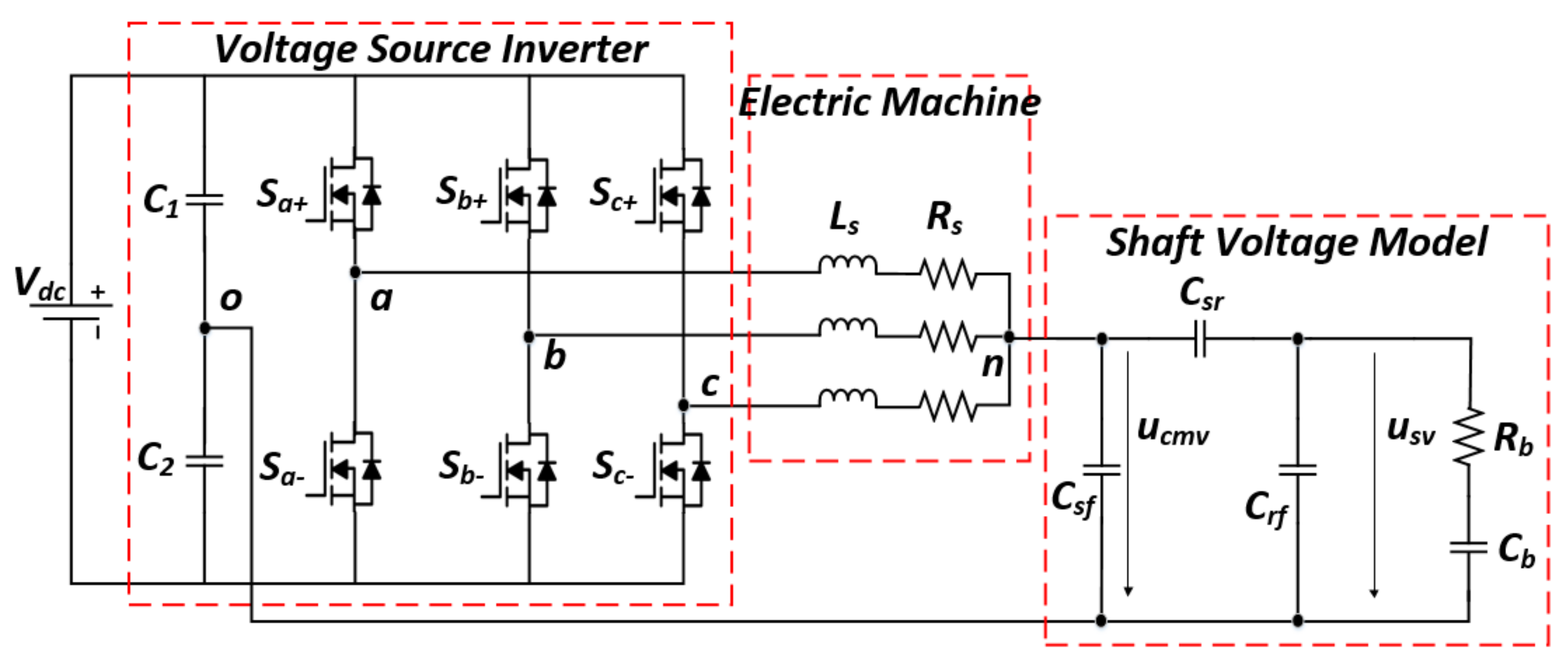
Figure 1. Topology of the vehicular electric drive system.
Wevj 13 00005 g001
Figure 2. Two types of voltage sectors division: (a) conventional SVPWM; (b) TSPWM.
Wevj 13 00005 g002
Figure 3. Vector constructing method of TSPWM: (a) low region; (b) high region.
Wevj 13 00005 g003
Figure 4. Comparison of CMV: (a) SVPWM in voltage sector A1; (b) low region of TSPWM in voltage sector B1; (c) high region of TSPWM in voltage sector B1.
Wevj 13 00005 g004
Figure 5. Discontinuous switching between two different sectors in TSPWM: (a) low region; (b) high region.
Wevj 13 00005 g005
Figure 6. Solution for discontinuous switching in TSPWM: (a) low region; (b) high region.
Wevj 13 00005 g006
Figure 7. Zero-voltage time interval between line-to-line voltage pulse reversals in SVPWM.
Wevj 13 00005 g007
Figure 8. Zero-voltage time interval between line-to-line voltage pulse reversals in TSPWM in different regions: (a) low region; (b) medium region (modulation factor equals to 0.61); (c) high region.
Wevj 13 00005 g008
Figure 9. Solution for the small zero-voltage time interval between line–line pulse reversals.
Wevj 13 00005 g009
Figure 10. Comparison of common voltages with SVPWM and TSPWM in low modulation region (M = 0.2): (a) SVPWM; (b) TSPWM; (c,d) are the enlarge views of (a,b), respectively.
Wevj 13 00005 g010
Figure 11. Comparison of common voltages with SVPWM and TSPWM in high modulation region (M = 0.8): (a) SVPWM; (b) TSPWM; (c,d) are the enlarge views of (a,b), respectively.
Wevj 13 00005 g011
Figure 12. Comparison of shaft voltages with SVPWM and TSPWM in low modulation region (M = 0.2), respectively: (a) SVPWM, (b) TSPWM.
Wevj 13 00005 g012
Figure 13. Comparison of shaft voltages with SVPWM and TSPWM in high modulation region (M = 0.8), respectively: (a) SVPWM, (b) TSPWM.
Wevj 13 00005 g013
Figure 14. TSPWM without zero-voltage time interval optimization (M = 0.6): (a) common voltage; (b) line–line voltage; (c) enlarge view of line–line voltage.
Wevj 13 00005 g014
Figure 15. TSPWM with zero-voltage time interval optimization (M = 0.6): (a) common voltage; (b) line–line voltage; (c) enlarge view of line–line voltage.
Wevj 13 00005 g015
Table 1. Parameters of the simulation platform.
ParametersValueParametersValue
DC link voltage360 VCsf11 nf
Switching frequency10 kHzCsr33 pf
Machine speed6000 rpmCrf1.65 nf
Phase current200 ACb300 pf
Simulation step1 × 10−6 sRb3.2 Ω
Publisher’s Note: MDPI stays neutral with regard to jurisdictional claims in published maps and institutional affiliations.

