
Optical and Electrochemical Properties of a Nanostructured ZnO Thin Layer Deposited on a Nanoporous Alumina Structure via Atomic Layer Deposition
 ,
,  ,
,  , and
, and 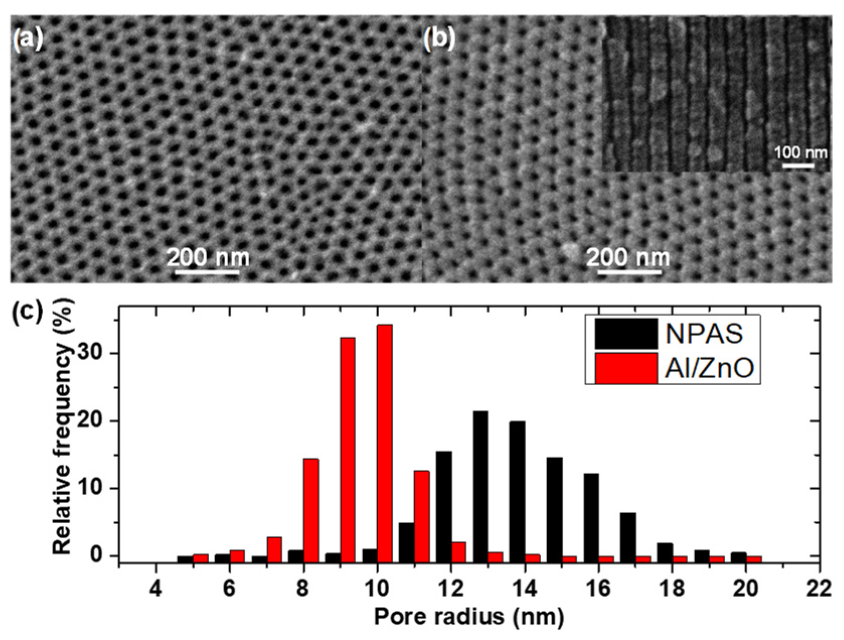
Abstract
:1. Introduction
2. Materials and Methods
2.1. Material Preparation
2.2. Scanning Electron Microscopy, X-ray Diffraction and Contact-Angle Measurements
2.3. Optical Characterization
2.4. Electrochemical Characterization of the Electrolyte–Al/ZnO Nanoporous Film System
3. Results
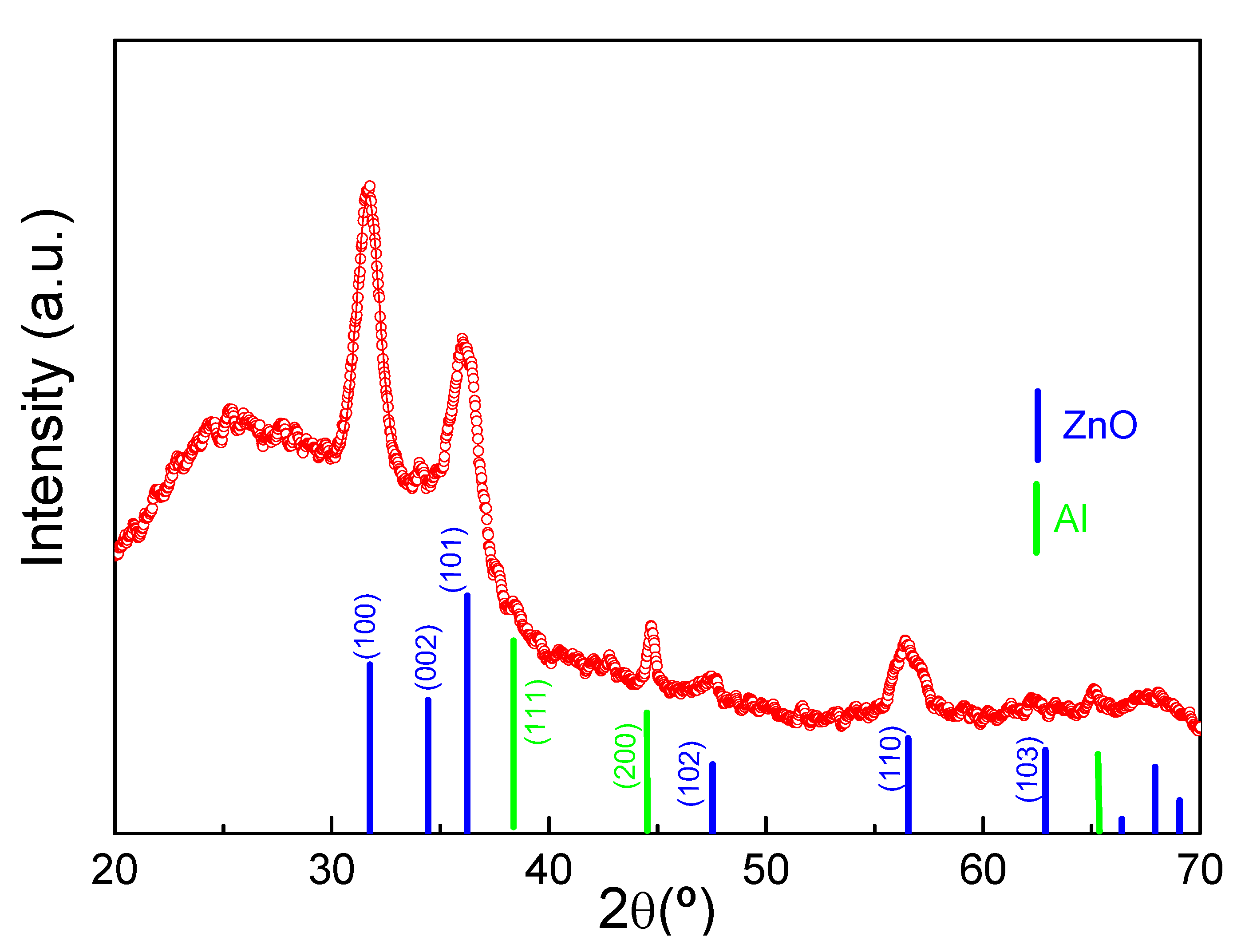
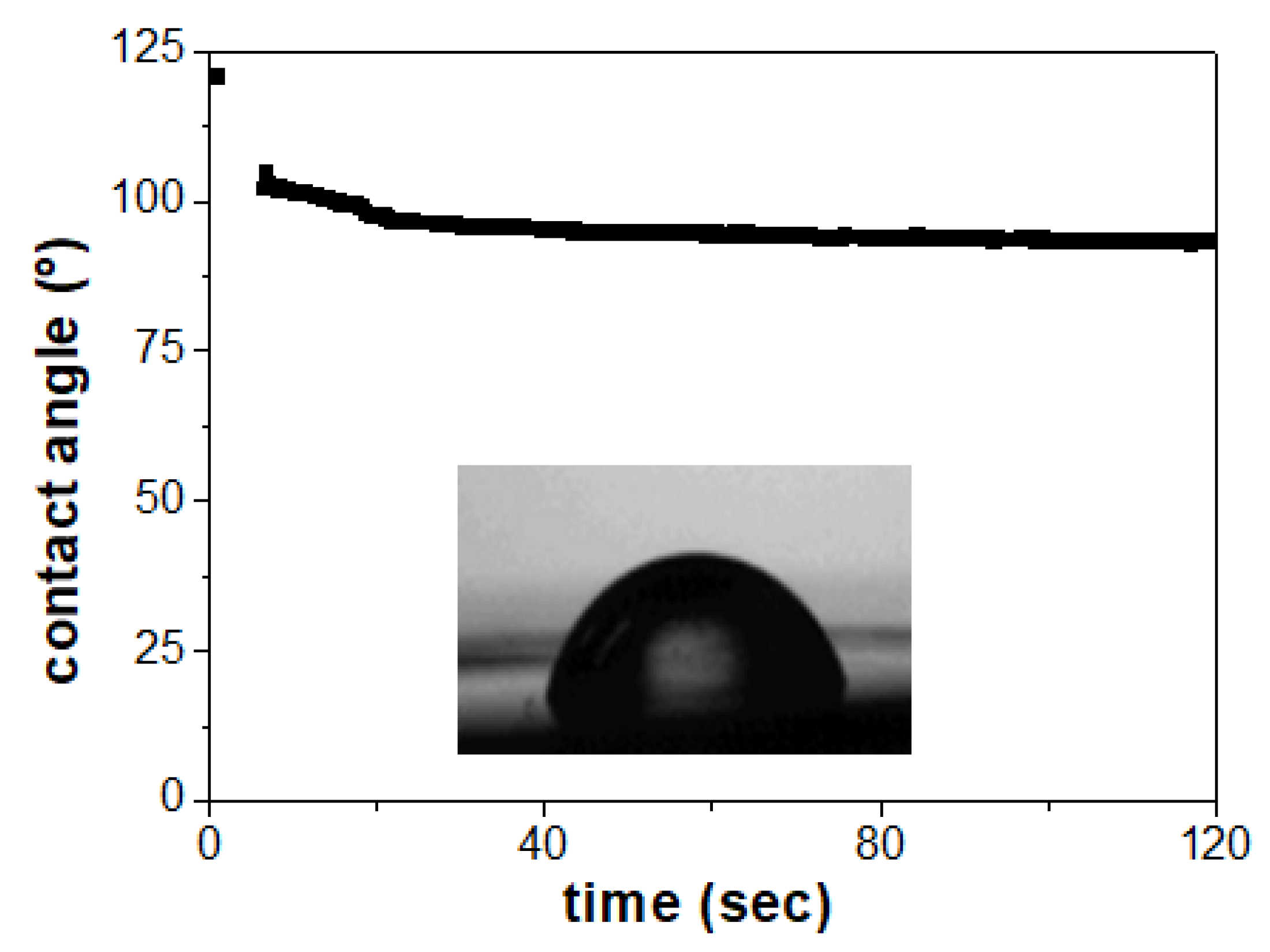
3.1. Microstructural Properties
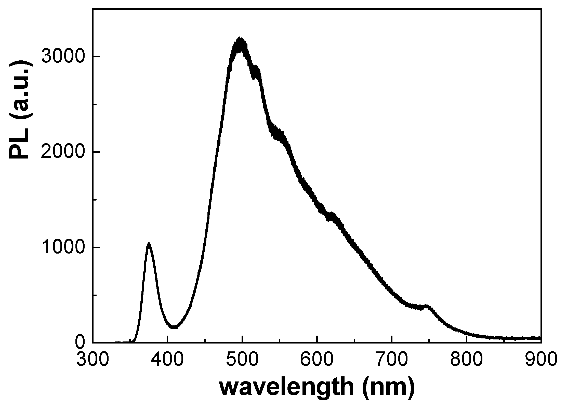
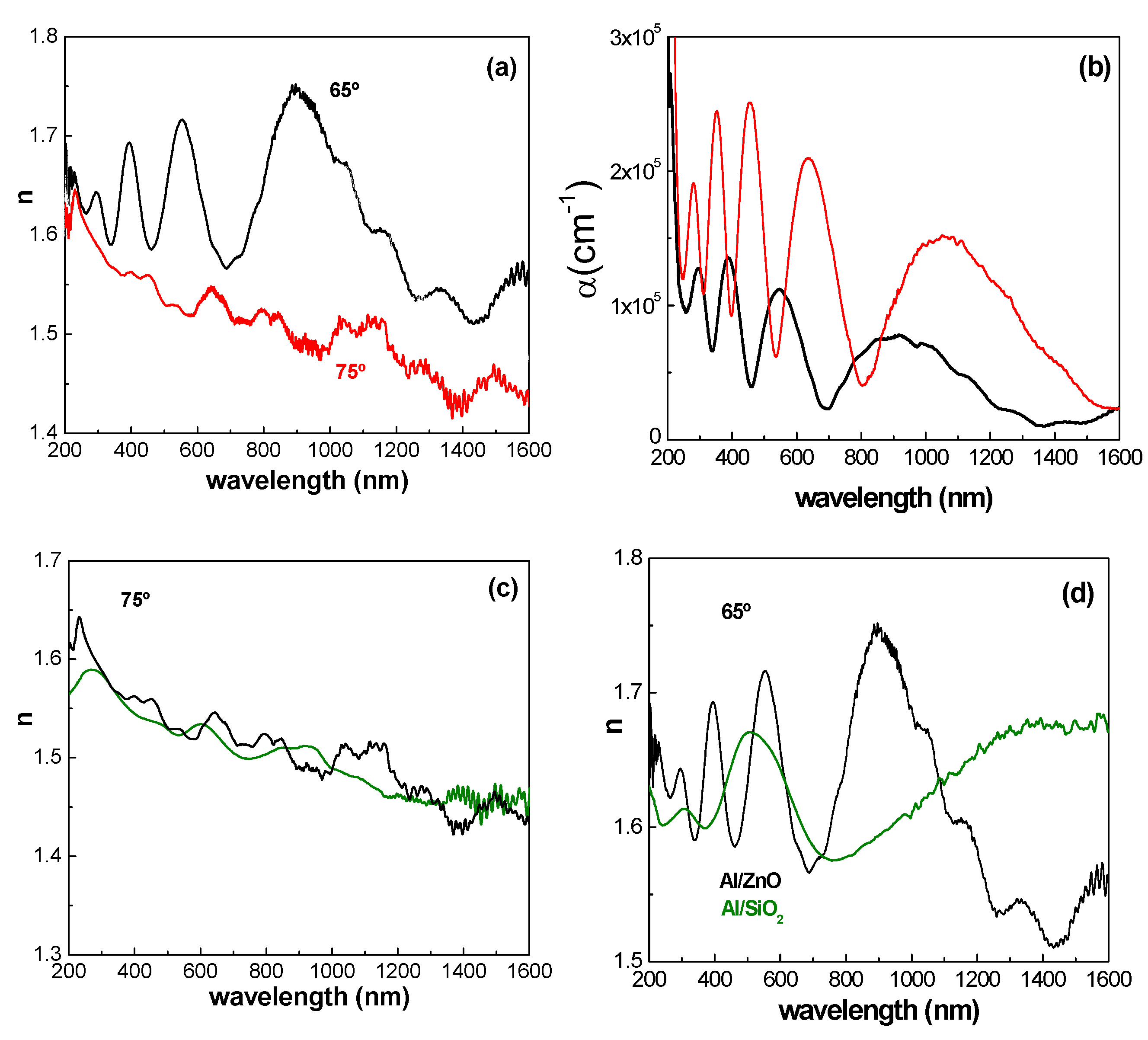
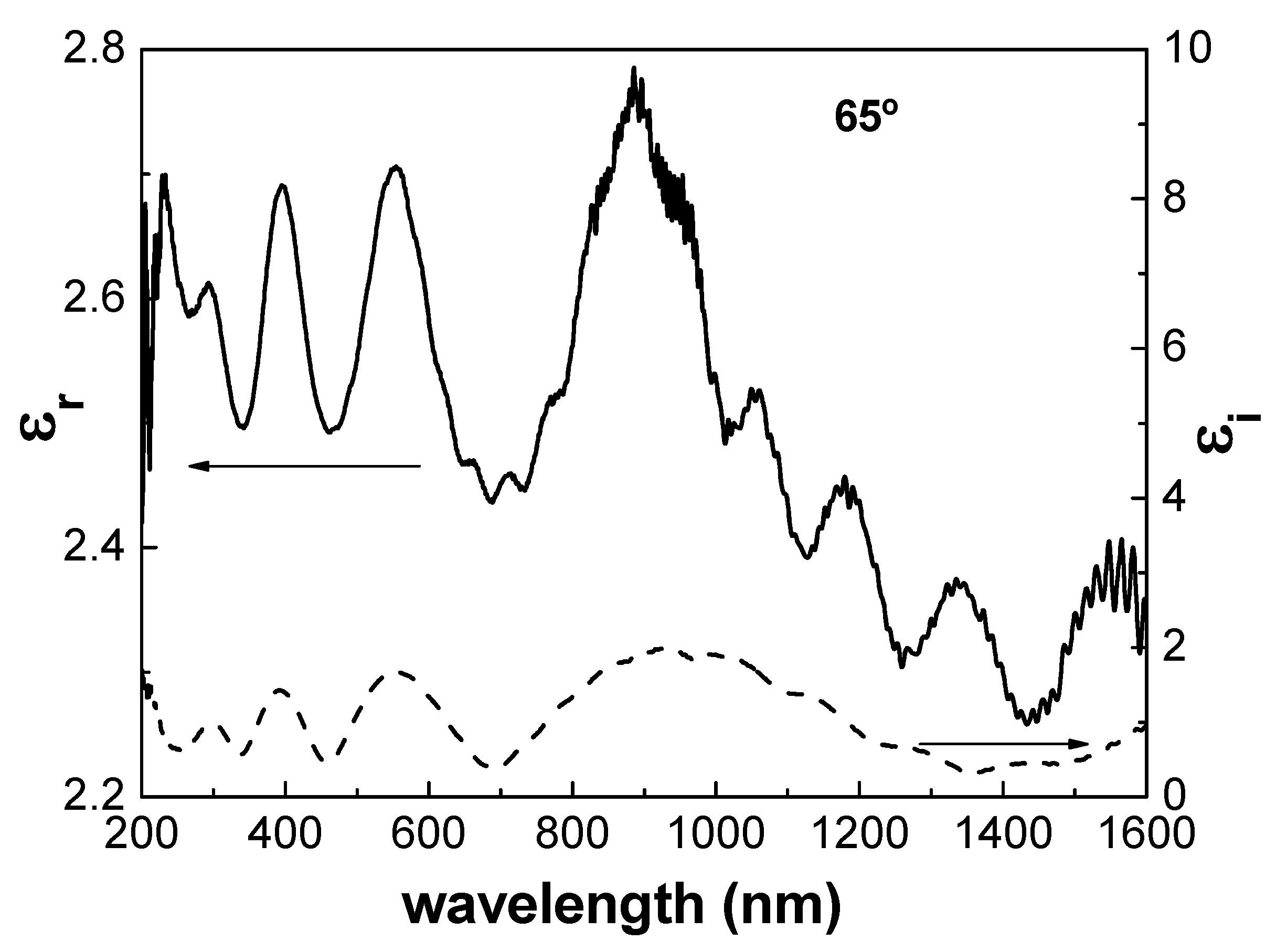
3.2. Optical Characterization
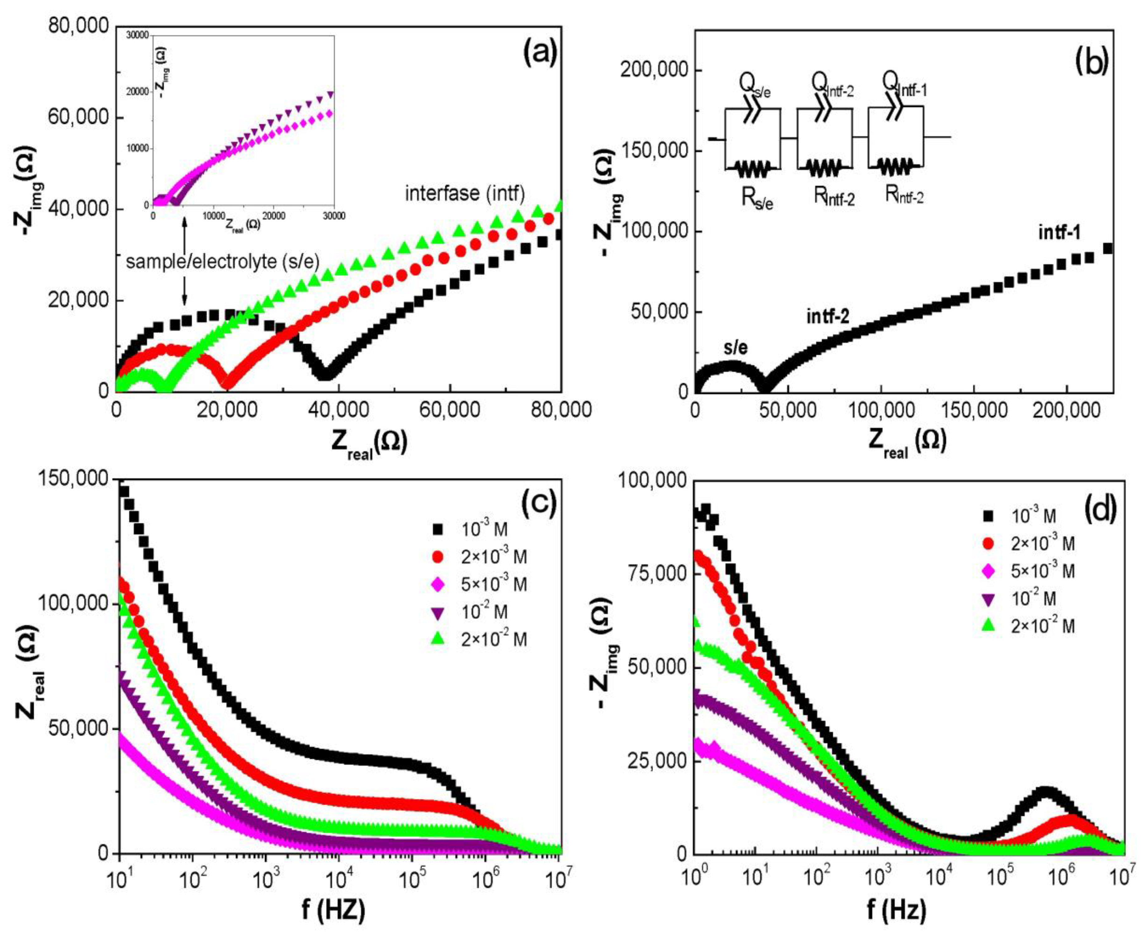
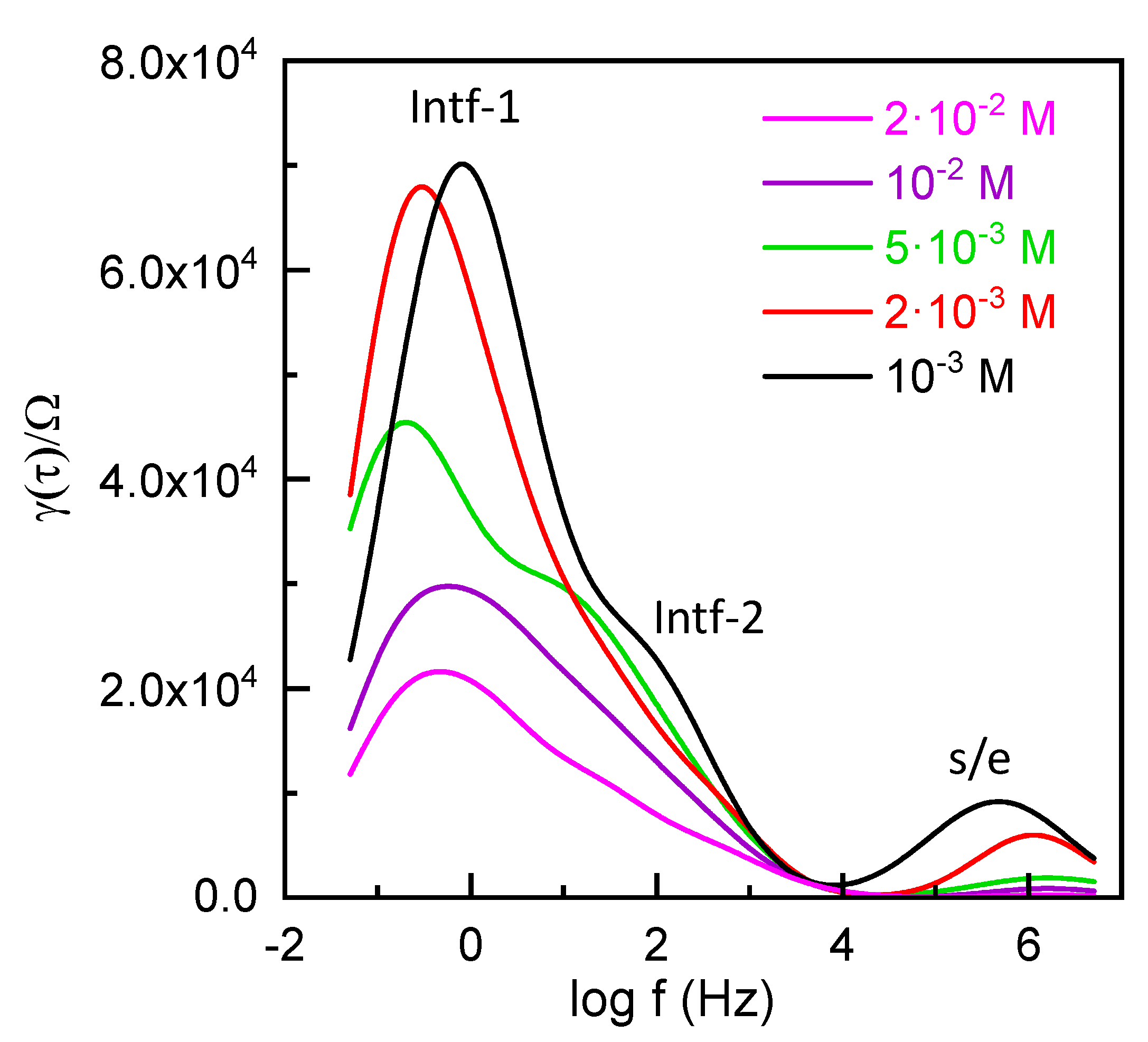
3.3. Electrochemical Characterization of the Al/ZnO Nanoporous Film
4. Conclusions
Supplementary Materials
Author Contributions
Funding
Institutional Review Board Statement
Informed Consent Statement
Data Availability Statement
Acknowledgments
Conflicts of Interest
References
- Masuda, H.; Fukuda, K. Ordered Metal Nanohole Arrays Made by a Two-Step Replication of Honeycomb Structures of Anodic Alumina. Science 1995, 268, 1466–1468. [Google Scholar] [CrossRef] [PubMed]
- Nielsch, K.; Choi, J.; Schwirn, K.; Wehrspohn, R.B.; Gösele, U. Self-ordering Regimes of Porous Alumina: The 10% Porosity Rule. Nano Lett. 2002, 2, 677–680. [Google Scholar] [CrossRef]
- Lee, W.; Park, S.J. Porous Anodic Aluminium Oxide: Anodization and Templated Synthesis of Functional Nanostructures. Chem. Rev. 2014, 15, 7487–7556. [Google Scholar] [CrossRef] [PubMed]
- Kipke, S.; Schmid, G. Nanoporous alumina membranes as diffusion controlling systems. Adv. Funct. Mater. 2004, 14, 1184–1187. [Google Scholar] [CrossRef]
- Hohlbein, J.; Steinhart, M.; Schiene-Fisher, C.; Benda, A.; Hof, M.; Hübner, C.G. Confined diffusion in ordered nanoporous alumina membranes. Small 2007, 3, 380–385. [Google Scholar] [CrossRef] [PubMed]
- Ren, C.; Fang, H.; Gu, J.; Winnubst, L.; Chen, C. Preparation and characterization of hydrophobic alumina planar membranes for water desalination. J. Eur. Ceram. Soc. 2015, 35, 723–730. [Google Scholar] [CrossRef]
- Ruiz-Clavijo, A.; Caballero-Calero, O.; Martín-González, M. Revisiting anodic alumina templates: From fabrication to applications. Nanoscale 2021, 13, 2227–2265. [Google Scholar] [CrossRef]
- Domagalski, J.T.; Xifre-Perez, E.; Marsal, L.F. Recent Advances in Nanoporous Anodic Alumina: Principles, Engineering, and Applications. Nanomaterials 2021, 11, 430. [Google Scholar] [CrossRef]
- Law, C.S.; Lim, S.Y.; Abell, A.D.; Voelcker, N.H.; Santos, A. Nanoporous Anodic Alumina Photonic Crystals for Optical Chemo- and Biosensing: Fundamentals, Advances, and Perspectives. Nanomaterials 2018, 8, 788. [Google Scholar] [CrossRef]
- Hedrich, C.; Burson, A.R.; González-García, S.; Vega, V.; Prida, V.M.; Santos, A.; Blick, R.H.; Zierold, R. Enhancing the Photocatalytic Activity by Tailoring an Anodic Aluminum Oxide Photonic Crystal to the Semiconductor Catalyst: At the Example of Iron Oxide. Adv. Mater. Interfaces 2023, 10, 2300615. [Google Scholar] [CrossRef]
- George, S.M. Atomic Layer Deposition: An Overview. Chem. Rev. 2010, 110, 111–131. [Google Scholar] [CrossRef] [PubMed]
- Coll, M.; Napari, M. Atomic layer deposition of functional multicomponent oxides. APL Mater. 2019, 7, 110901. [Google Scholar] [CrossRef]
- Johnson, R.W.; Hultqvist, A.; Bent, S.F. A brief review of atomic layer deposition: From fundamentals to applications. Mater. Today 2014, 17, 236–246. [Google Scholar] [CrossRef]
- Richeyy, N.E.; de Paula, C.; Bent, S.F. Understanding chemical and physical mechanisms in atomic layer deposition. J. Chem. Phys. 2020, 152, 040902. [Google Scholar] [CrossRef] [PubMed]
- Cuevas, A.L.; Martínez de Yuso, M.V.; Vega, V.; González, A.S.; Prida, V.M.; Benavente, J. Influence of ALD Coating Layers on the Optical Properties of Nanoporous Alumina-Based Structures. Coatings 2019, 9, 43. [Google Scholar] [CrossRef]
- González, A.S.; Vega, V.; Cuevas, A.L.; Martínez de Yuso, M.V.; Prida, V.M.; Benavente, J. Surface Modification of Nanoporous Anodic Alumina during Self-Catalytic Atomic Layer Deposition of Silicon Dioxide from (3-Aminopropyl) Triethoxysilane. Materials 2021, 14, 5052. [Google Scholar] [CrossRef]
- Romero, V.; Vega, V.; García, J.; Zierold, R.; Nielsch, K.; Prida, V.M.; Benavente, J. Changes in Morphology and Ionic Transport Induced by ALD SiO2 Coating of Nanoporous Alumina Membranes. ACS Appl. Mater. Interfaces 2013, 5, 3556–3564. [Google Scholar] [CrossRef]
- Vázquez, M.V.; Romero, V.; Vega, V.; García, J.; Prida, V.M.; Hernando, B.; Benavente, J. Morphological, chemical surface and diffusive transport characterizations of a nanoporous alumina membrane. Nanomaterials 2015, 5, 2192–2202. [Google Scholar] [CrossRef]
- Cuevas, A.L.; Martínez de Yuso, M.V.; Gelde, L.; González, A.S.; Vega, V.; Prida, V.M.; Benavente, J. Chemical, optical and transport characterization of ALD modified nanoporous alumina based structures. J. Ind. Eng. Chem. 2020, 152, 040902. [Google Scholar] [CrossRef]
- Bluhm, E.A.; Bauer, E.; Chamberlin, R.M.; Anbey, K.D.; Younhg, J.S.; Jarvinen, G.D. Surface effects on cation transport across porous alumina membranes. Langmuir 1999, 15, 8668–8672. [Google Scholar] [CrossRef]
- Treccani, L.; Klein, T.Y.; Meder, F.; Pardum, K.; Rezwan, K. Functionalized ceramics for biomedical, biotechnological and environmental applications. Acta Biomater. 2013, 9, 7115–7150. [Google Scholar] [CrossRef] [PubMed]
- Westover, A.; Li, M.; Pint, C.L. Surface engineering of nanomaterials for improved energy storage—A review. Chem. Eng. Sci. 2016, 154, 3–19. [Google Scholar]
- Wang, J.; Malgras, V.; Sugahara, Y.; Yamauchi, Y. Electrochemical energy storage performence of 2D nanoarchitectured hybrid materials. Nat. Commun. 2021, 12, 3563. [Google Scholar] [CrossRef] [PubMed]
- Klingshirn, C.F.; Meyer, B.K.; Waag, A.; Hoffmann, A.; Geurts, J. Zinc Oxide: From Fundamental Properties towards Novel Applications; Springer: Berlin/Heidelberg, Germany, 2010. [Google Scholar]
- Litton, C.W.; Collins, T.C.; Reynolds, D.C.; Capper, P.; Kasap, S.; Willoughby, A. Zinc Oxide Materials for Electronic and Optoelectronic Device Applications; Wiley: Hoboken, NJ, USA, 2011. [Google Scholar]
- Di Mauro, A.; Fragalà, M.E.; Priviteraa, V.; Impellizzeri, G. ZnO for application in photocatalysis: From thin films to nanostructures. Mater. Sci. Semicond. Process. 2017, 69, 44–51. [Google Scholar] [CrossRef]
- Zheng, H.; Zhang, R.-J.; Li, D.-H.; Wang, S.-Y.; Zheng, Y.-X.; Li, M.-J.; Hu, Z.-G.; Dai, N.; Chen, L.-Y. Optical properties of Al-doped ZnO films in the infrared region and their absorption applications. Nanoscale Res. Lett. 2018, 13, 14. [Google Scholar] [CrossRef] [PubMed]
- Park, K.-H.; Sun, P.-F.; Kang, E.H.; Han, G.D.; Kim, B.J.; Jang, Y.; Lee, S.-H.; Shim, J.H.; Park, H.-D. Photocatalytic and anti-biofouling performance of nanoporous ceramic membranes treated by atomic layer deposited ZnO. Sep. Purif. Technol. 2021, 272, 118935. [Google Scholar] [CrossRef]
- Hwang, D.-K.; Oh, M.-S.; Lim, J.-H.; Park, S.-J. ZnO thin films and ligtht-emitting diodes. J. Phys. D Appl. Phys. 2007, 40, R387–R412. [Google Scholar] [CrossRef]
- Mosquera, A.A.; Horwat, D.; Rashkovskiy, A.; Kovalev, A.; Miska, P.; Wainstein, D.; Albella, J.M.; Endrino, J.L. Exciton and core-level electron confinement effects in transparent ZnO thin films. Sci. Rep. 2013, 3, 1714. [Google Scholar] [CrossRef]
- Hahm, J. Zinc oxide nanomaterials for biomedical fluorescence detection. J. Nanosci. Nanotechnol. 2014, 14, 475–486. [Google Scholar] [CrossRef]
- Dash, R.; Mahender, C.; Sahoo, P.K. Preparation of ZnO layer for solar cell application. Mater. Today Proc. 2021, 44, 161–164. [Google Scholar] [CrossRef]
- Wibowo, A.; Marsudi, M.A.; Amal, M.I.; Ananda, M.B.; Stephanie, R.; Ardy, H.; Diguna, L.J. ZnO nanostructured materials for emerging solar cell applications. RSC Adv. 2020, 10, 42838–42859. [Google Scholar] [CrossRef] [PubMed]
- Cridling, Q.; Charriere, R.; Jamon, D.; Lenci, M.; Pedeferri, M.P.; Delafosse, D. Anodized titanium oxide thickness estimation with ellipsometry, reflectance spectra extrema positions and electronic imaging: Importance of the interfaces electromagnetic phase-shift. Thin Solid Film. 2020, 709, 138181. [Google Scholar] [CrossRef]
- Sun, Y.-S.; Zhu, X. Ellipsometry-based biosensor for label-free detection of biomolecular interactions in microarray format. Sens. Mater. 2013, 25, 673–688. [Google Scholar]
- Zhao, Z.; Shi, S.; Cao, H.; Li, Y. Electrochemical impedance spectroscopy and surface properties characterization of anion-exchange membrane fouled by sodium dodecyl sulfate. J. Membr. Sci. 2017, 530, 220–231. [Google Scholar] [CrossRef]
- Kozmai, A.; Sarapulova, V.; Sharafan, M.; Melkonian, K.; Rusinova, T.; Kozmai, Y.; Pismenskaya, N.; Dammak, L.; Nikonenko, V. Electrochemical Impedance Spectroscopy of Anion-Exchange Membrane AMX-Sb Fouled by Red Wine Components. Membranes 2021, 11, 2. [Google Scholar] [CrossRef] [PubMed]
- Mulder, M. Basic Principles of Membrane Technology; Kluwner Academic Publishers: Dordrecht, The Netherland, 1991. [Google Scholar]
- Guziewicz, E.; Kowalik, I.A.; Godlewski, M.; Kopalko, K.; Osinniy, V.; Wójcik, A.; Yatsunenko, S.; Łusakowska, E.; Paszkowicz, W.; Guziewicz, M. Extremely low temperature growth of ZnO by atomic layer deposition. J. Appl. Phys. 2008, 103, 033515. [Google Scholar] [CrossRef]
- Schneider, C.A.; Rasband, W.S.; Eliceiri, K.W. NIH Image to ImageJ: 25 years of image analysis. Nat. Methods 2012, 9, 671–675. [Google Scholar] [CrossRef]
- Amelo, B. Pert HighScore Plus, Version 3.0 ed.; PNAnalytical B.V.: Almelo, The Netherlands, 2012. [Google Scholar]
- Tompkins, G.; Hilfiker, J.N. Spectroscopic Ellipsometry: Practical Application to Thin Film Characterization, 1st ed.; Momentum Press: New York, NY, USA, 2016; pp. 57–70. [Google Scholar]
- Macdonald, J.R.; Johnson, W.B. Fundamentals of Impedance Spectroscopy. In Impedance Spectroscopy: Theory, Experiment, and Applications, 3rd ed.; Barsoukov, E., Ed.; Wiley Online Library: Hoboken, NJ, USA, 2018. [Google Scholar] [CrossRef]
- Wan, T.H.; Saccoccio, M.; Chen, C.; Ciucci, F. Influence of the Discretization Methods on the Distribution of Relaxation Times Deconvolution: Implementing Radial Basis Functions with DRTtools. Electrochim. Acta 2015, 184, 483–499. [Google Scholar] [CrossRef]
- Albertsson, J.; Abrahams, S.C.; Kvick, A. Atomic displacement, anharmonic thermal vibration, expansivity and pyroelectric coefficient thermal dependences in ZnO. Acta Crystallogr. 1989, B45, 35–40. [Google Scholar] [CrossRef]
- Yuste, M.; Escobar Galindo, R.; Martínez Sacristán, O.; Mínguez-Bacho, I.; Rodriguez, S.; Hernández-Vélez, M.; Sánchez, O. Structural and optical characterization of nanostructured ZnO grown on alumina templates. Mater. Res. Express 2014, 1, 045028. [Google Scholar] [CrossRef]
- Jogi, A.; Ayana, A.; Rajendra, B.V. Modulation of optical and photoluminescence properties of ZnO thin films by Mg dopant. J. Mater. Sci. Mater. Electron. 2023, 34, 624. [Google Scholar] [CrossRef]
- Fang, Z.; Wang, Y.; Peng, X.; Liu, X.; Zhen, C. Structural and optical properties of ZnO films grown on the AAO templates. Mater. Lett. 2003, 57, 4187–4190. [Google Scholar] [CrossRef]
- Postava, K.; Sueki, H.; Aoyama, M.; Yamaguchi, T.; Murakami, K.; Igasaki, Y. Doping effects on optical properties of epitaxial ZnO layers determined by spectroscopic ellipsometry. App. Surf. Sci. 2001, 175–176, 543–548. [Google Scholar] [CrossRef]
- Ferré-Borrull, J.; Xifré-Pérez, E.; Pallarès, J.; Marsal, L.F. Optical Properties of Nanoporous Anodic Alumina and Derived Applications. In Nanoporous Alumina; Losic, D., Santos, A., Eds.; Springer International Publisher: Berlin/Heidelberg, Germany, 2015. [Google Scholar]
- Caglar, M.; Ilican, S.; Caglar, Y.; Yakuphanoglu, F. Electrical conductivity and optical properties of ZnO nanostructyred thin films. Appl. Surf. Sci. 2009, 255, 4491–4496. [Google Scholar] [CrossRef]
- Gadallh, A.-S.; El-Nahass, M. Structural, optical constant and photoluminescence of ZnO thin film grown by sol-gel spin coating. Adv. Condens. Matter Phys. 2013, 2013, 234546. [Google Scholar] [CrossRef]
- Coster, H.G.L.; Kim, K.J.; Dahlan, K.; Smith, J.R.; Fell, C.J.D. Characterisation of ultrafiltration membranes by impedance spectroscopy. I. Determination of the separate electrical parameters and porosity of the skin and sublayers. J. Membr. Sci. 1992, 66, 19–26. [Google Scholar] [CrossRef]
- Benavente, J.; Jonsson, G. Characterization of active and porous sublayers of composite membranes from hydrodynamic and electrical measurements with different electrolytes. Desalination 2006, 200, 364. [Google Scholar] [CrossRef]
- Efligenir, A.; Fievet, P.; Déon, S.; Salut, R. Characterization of the isolated active layer of a NF membrane by electrochemical impedance spectroscopy. J. Membr. Sci. 2015, 477, 172–182. [Google Scholar] [CrossRef]
- Quattrocchi, E.; Wan, T.H.; Belotti, A.; Kim, D.; Pepe, S.; Kalinin, S.V.; Ahmadi, M.; Ciucci, F. The deep-DRT: A deep neural network approach to deconvolve the distribution of relaxation times from multidimensional electrochemical impedance spectroscopy data. Electrochim. Acta 2021, 392, 139010. [Google Scholar] [CrossRef]
- Ramos-Barrado, J.R.; Benavente, J.; Bruque, S.; Martínez, M. Impedance spectroscopy study with Ca(UO2PO4)210.5H2O films. J. Colloid Interface Sci. 1995, 170, 550–554. [Google Scholar] [CrossRef]


Disclaimer/Publisher’s Note: The statements, opinions and data contained in all publications are solely those of the individual author(s) and contributor(s) and not of MDPI and/or the editor(s). MDPI and/or the editor(s) disclaim responsibility for any injury to people or property resulting from any ideas, methods, instructions or products referred to in the content. |
© 2024 by the authors. Licensee MDPI, Basel, Switzerland. This article is an open access article distributed under the terms and conditions of the Creative Commons Attribution (CC BY) license (https://creativecommons.org/licenses/by/4.0/).
Share and Cite
Cuevas, A.L.; Dominguez, A.; Zamudio-García, J.; Vega, V.; González, A.S.; Marrero-López, D.; Prida, V.M.; Benavente, J. Optical and Electrochemical Properties of a Nanostructured ZnO Thin Layer Deposited on a Nanoporous Alumina Structure via Atomic Layer Deposition. Materials 2024, 17, 1412. https://doi.org/10.3390/ma17061412
Cuevas AL, Dominguez A, Zamudio-García J, Vega V, González AS, Marrero-López D, Prida VM, Benavente J. Optical and Electrochemical Properties of a Nanostructured ZnO Thin Layer Deposited on a Nanoporous Alumina Structure via Atomic Layer Deposition. Materials. 2024; 17(6):1412. https://doi.org/10.3390/ma17061412
Chicago/Turabian StyleCuevas, Ana L., Antonia Dominguez, Javier Zamudio-García, Victor Vega, Ana Silvia González, David Marrero-López, Victor M. Prida, and Juana Benavente. 2024. "Optical and Electrochemical Properties of a Nanostructured ZnO Thin Layer Deposited on a Nanoporous Alumina Structure via Atomic Layer Deposition" Materials 17, no. 6: 1412. https://doi.org/10.3390/ma17061412